Note: Descriptions are shown in the official language in which they were submitted.
13097a~ E-1068
LAEEL NO. B132 074 25Y~
I~Ul)lO FREQUENCY POWER
AMPLIFIER WITH IMPROVED ClRCUIT TOPOLOGY
B~CKGROUND OF THE INVENTION
1. Field of the Invention
This invention relates to improvements in vacuum-tube~
audlo power amplifier circuit topology.
2. Description of the Prior Art
Examples of prior art audio power amplifiers are the
amplifiers described in Hafler, 120 Watts of ~li-Fi Power,
10 Radio & TV News, February 1959, pages 118-120, and
; Hafler, A 60-Watt "Ultra-Llnear" Amplifier", Radio & TV
News, February 1955, page 45 et seq.
The problem with audio power amplifiers using the prior
art circuit topology described in these references is that
they possess certain performance deficiencies. FirstlyJ the
direct-coupled voltage amplifier-phase inverter input
circuit has poor current stability, so that variations in
tube characteristics or tube supply voltages affect
performance. Secondly, the phase inverter stage has limited
.
13~97~
- 2 ~ 63129-88
drive capability to the power amplifier output stage, which results
in higher distortion and less than optimum power output. The
present invention overcomes these difficulties by utilizing a
novel input circuit topology incorporating direct current feedback.
Also included in the invention input circuit is a low impedance
phase inverter having enhanced drive capability. The higher drive
capability reduces distortion and also yields a higher power output
by ensuring adequate drive power to the push-pull output stage.
BRIEF DESCRIPTION OF THE DRAWINGS
10Figure 1 is a schematic diagram of a prior art vol-
tage amplifier and phase inverter;
Figure 2 is a schematic diagram of a prior art voltage
amplifier and phase inverter;
Figure 3 is a schematic diagram of another prior art
voltage amplifier and phase inverter;
Figure 4 is a schematic diagram of a voltage amplifier
and phase inverter of the invention;
Figure 5 is a detailed schematic diagram of the present
voltage amplifier and phase inverter of the invention;
20Figure 6 is a schematic diagram of a split-load phase
inverter connected to a load;
Figure 7 is a schematic diagram of the signal-handling
portion of a power amplifier;
Figure 8 is a schematic diagram of another embodiment
of the voltage amplifier and phase inverter of the invention; and
Figure 9 is a schematic diagram of another embodiment
13~3~3~
- 2a - 63129-88
of the voltage amplifier and phase inverter of the invention.
A typical prior art input circuit partial schematic
diagram is shown in Figure 1. The voltage amplifier 11 is a
triode, or pentode, vacuum tube operated as a high-gain voltage
amplifier, The triode vacuum tube 13 is a well-known split-load
phase inverter, which has outputs of equal voltage but opposite
phase at terminals 15 and 17.
Figure 2 is a more detailed schematic diagram of a
prior art input circuit. Resistor 21 is a grid leak resistor.
The capacitor 23 is a bypass capacitor with reactance at least
one order of magnitude lower than the resistance of screen-grid
resistor 25 at the lowest audio frequency of 20 Hz. Resistors 25,
27, and 29 determine the direct current operating point for tubes
13 and 31. This operating point is generally set so as to
cause the no-signal direct current voltage drops across tube 13
and both resistors l9a, l9b tb be approximately
130~7~
3 E-1068
equal. Stated another way, the voltage drop across each
resistor 19a, 19~ is equal to one-half the voltage drop
across tube 13. As is well understood by those skilled in
the art, this ensures maximum output voltage at the phase
inverter output terminals 15 and 17.
Since no direct current feedback is employed from tube
13 to tube 31 in the circuit of Figure 2, the direct current
operating point of the circuit depends on the
characteristics of pentode vacuum tube 31 and triode vacuum
tube 13, as well as on the values of resistors 25, 27, and
29. The resistance values of resistors 25, 27 and 29
generally remain stable over time, but the characteristics
of the tubes change with age. The aging causes a random
drift of the direct current operating point of the circuit
a~s the tubes age. The direct current operating point also
drifts if filament or plate power supply voltages change,
since a change in either aforementioned power supply voltage
affects tube characteristics. Thus, the optimum operating ;~
point of the circuit would occur only by accident; usually
an error exists which is sufficiently large to reduce
circuit performance to less than optimum.
Another prior-art amplifier input circuit is shown in
Fig. 3. This circuit differs from that shown in Fig. 2
because the circuit in Fig. 3 has the screen grid of pentode
31 connected through resistor 33 to the cathode of phase
inverter tube 13 instead of to the B+ supply.
Resistor 21 is a grid leak resistor, capacitor 23 is a
bypass capacitor with reactance at least one order of
13 0 ~ rl ~ ~
I E-1068
magnitu~e lower than the resistance of screen grid resistor
33 at the lowest audio frequency o~ 20 Hz. Resistors 27, 29
and 33 determine the direct current operating point for
- tubes 31 and 13. This operating point is generally set so
as to cause the no signal direct current voltage across tube
13 and the sum of the direct current voltages across the two
resistors l9a, 19b to be approximately equal.
; Direct current feedback from tube 13 to tube 31 is
.,,
accomplished by connecting resistor 33 between the screen
grid of 3] and the cathode of 13. Since this feedback
connection unbalances the phase inverter outputs, a resistor
36 is added in series with the cathode load resistor l9-b to
compensate for the unbalance.
The mode of operation for the direct current feedback
is explained hereinafter in the description of the preferred
embodiments. Also explained is an improve~l means whereby
the present invention overcomes the phase inverter unbalance
problem of the prior art circuit of Fig. 3.
SUMMARY OF qlHE INVENI`~ON
l~he present invention is an audio frequency power
amplifier input circuit. The circuit employs a split load
phase inverter to provide outputs of equal voltage but
opposite phase at its output terminals. In order to
stabilize the direct current operating pOillt against
variations in tube characteristics or supply voltages, the
present invention employs a direct current feedback circuit
to the voltage amplifier circuit which normally feeds the
I signals to the split load phase inverter. In addition, the
13~756
- 5 - 63129-88
present invention employs two transi.stor emitter-follower circuits
which enhance the drive capability of the phase inverter. The
foregoing mentioned higher drive capacity reduces distortion and
also yields a higher power output by ensuring adequate drive power
to a push-pull output stage.
The invention may be summarized, according to one as-
pect, as an audio power amplifier input circuit comprising in com-
bination: split-load phase inverter circuit means 13, l9a, l9b,
l9c, l9d, 47, 49 having a preferred direct current operating point
and formed to have electrical current control means to regulate
the electrical current passing therethrough; voltage amplifier
circuit means 45 including voltage output means, whose voltage
value increases and alternatively decreases in response respective-
ly to decreased and alternatively increased electrical current
flow through said voltage amplifier circuit means, said voltage
amplifier circuit means further having a current control means to
regulate current passing therethrough; direct current feedback
circuitry means connected between said current control means of
said split-load phase inverter circuit means 13, l9a, l9b, l9c,
l9d, 47, 49 and both said voltage output means of said voltage
amplifier circuit means as well as said current control means of
said voltage amplifier circuit means 45 whereby when electrical
current flowing through said voltage amplifier circuit means is
reduced and alternatively increased, current flowing through said
split-load phase inverter circuit means will respectively be in-
creased and alternatively decreased to substantially maintain said
preferred direct current operating point of said split-load phase
inverter circuit means 13, l9a, l9b, l9c, l9d, 47, 49.
6 130~7~6 E-l06B
DBTAILED DESCRIPTION OF THE PR~FERRED EMBO~IMENT
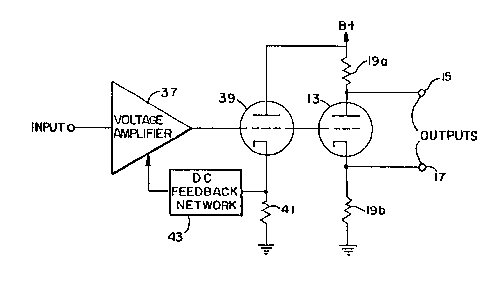
Consider Figure 4. Figure 4 depicts a version of the
present invention. A high gain triode cascode or pentode
voltage amplifier 37 is connected to two triode vacuum tubes
13 and 39. Triode 13 functions as a split-load phase
inverter, while triode 39 functions as a cathode follower.
Voltage aoross resistor 41, connected to cathode follower
39, is applied through a feedback network ~3 to voltage
amplifier 37.
A more detailed input circuit embodiment is shown
schematical]y in Figure 5. Dual triode vacuum tube 45 is
connected as the well-known cascode circuit with triode
section 45a functioning as a grounded-cathode first stage,
directly coupled to triode section 45b functioning as a
grounded-grid second stage. The cascode circuit has a high
gain-bandwidth product as well as low noise and distortion,
well-known to those s};illed in the art.
Resistor 21 is a grid-leak resistor. Capacitor 23 is a
bypass capacitor with reactance at least an order of
magnitude lower than the effective combined resistance to
ground of resistors 33, 35 and 41 at the lowest audio
frequency of 20 Hz. Cascode voltage amplifier 45 is direct-
coupled to the grids of triode cathode-follower 39 and
triode split-load phase inverter 13. Cathode follower 39
develops a voltage across resistor 41 which also appears
across voltage divider resistors 33 and 35. The junction of
resistor divider 33 and 35 is connected to the grid of
.
130~7~
7 E-106~
cascode triode 45b. The direct current operating point of
the enti.re circuit is set by the respective values of
resistors 27~ 29, 33, 35 and 4].. ~s explained hereinbefore,
in order to secure maxi.mum output voltage from the phase
inverter, the direct ~urrent operating point is adjusted so
that the no-si~nal di rect current voltage drops acros~ phase
inverter tuhe 13 and hoth equal-value load resistors l9a,
l9b are approximat~ly equal.
Feedback from tric,-le 39 t}~ro~gh resistor divi.der 33-35
to triode 45b serves to stahllize the direct current
operating point against vari.ations in tube characteristics
or power supply voltages. As an illustrative example,
assume that as tube 45 ages its transconductance drops.
Thi.s causes the plate current to drop maki.ng the voltage ~t
the plate of triode 45b rise. The voltage at the cathode of
cathode follower 3~ also ri.ses, and so the voltage rises
across the divider made up of resistors 33 and 35. Thus,
the vol.tage on the grid of triode 45b rises. This
i.ncreased bias on the grid of 45b increases the plate
current in triode 45, restoring circuit operation near to
its original di.rect current operating point. Other
variations in tube characteristics or power supply
voltages which wou]d tend to upset the optimum direct
. .
~3~7~
8 E-1068
current operating point of the circuit are corrected by the
feedback in a similar manner. The direct current feedback
employe(~ in the invention embodiment of Figure 5 tends to
maintain the direct current operating point of the amplifier
input circuit close to the optimum as tubes age or power
supply voltages change.
Transistors 47 and 49 serve to isolate the load
connected to terminals 15 and 17 from phase inverter tube
13. The split-load phase inverter ~3 has radically
0 different output impedances at each of its output terminals.
Referring to Figure 4 the output impedance at terminal 15 is
given by:
ZO= (Jl - 1)R, (1)
where ZO is the output impedance, ~u is the amplification
factor for a triode vacuum tube, and R is the resistance of
resistors 19a, l9b shown in Figure 4. The output impedance
at terminal 17 is given by:
ZO = (rp+ R)/(~ ~ 1), (2)
where rp is the plate resistance. For a typical triode such
as the commonly used type 12AU7 having
= 20
rp= 15 kilohms
with load resistor R equal to 33 kilohms, equation (1)
yields a value of output impedance at terminal 15 of:
ZO= (20 - 1)33 = 627 kilohms,
9 130~7~ E-1068
and equation 1 yields a value of output impedance at
terminal 17 of:
z~= (15000 + 33000)/(20 + 1) - 2300 ohms.
Optimum function of the split-load phase inverter
requires a load as seen at terminals 15 and 17 of at least
an order of magnitude hi~her than the highest output
impedance of the phase inverter itself, i.e., higher than
the output impedance of terminal 15.
In typical amplifier circuits the load seen by the
phase inverter will amount to about 100 kilohms. This load
condition is i]lustrated in Figure 6. The plate and cathode
of split-load phase inverter 13 are alternating current
coupled to each respective grid of output tubes 51a, 51b via
blocking capacitors 53a, 53b. The load seen by the phasq
inverter output terminals 15 and 17 consists of
grid-bias resistors 55a and 55b in combination with
the input resistance and reactance of output tubes 51a, 51b.
As explained immediately hereinbefore, this phase inverter
load impedance value is about 100 kilohms in typical
amplifier circuits.
The 100 kilohm load at the output tube grids is lower
than the output impedance of the phase inverter terminal 15
calculated hereinbefore as
Zc= 627 kilohms,
while terminal l7 has an output impedance of
ZO= 2300 ohms,
,
lo ~ 3 ~ 9 7 ~ ~ E-1068
much lower than tl~e typical 100 ki]ohm ].oad stated
hereinbefore. Thus the phase inverter 13 easily drives its
load from terminal ].7 but is less able to drive its load
from terminal 15. Distortion is increased and maximum
output voltage is reduced at terminal 15 with respect to
terminal 17. ThuS the phase inverter becomes unhalanced.
Performance would be improved if the output impeaance at
phase inverter output terminals 15 and 17 could be lowered.
Transistor emi.tter followers connected to the phase
inverter plate and cathode provi.de the desired lower output
impedances. Referring to Figure 5, the output impedance of
the phase inverter at terminal 15 with the emitter follower
is given by:
! Zo~ R (1 - a) (3)
15 where R is the output impedance of the phase inverter
without emitter fol.lower as calculated earlier;
627 kil.ohms,
and a is the common-base current gain of the transistor,
~ typi.cally
: 20 a = 0.98
yiel.ding an output impedance at terminal 15 of the circuit
in Figure 5, using equation (3) of:
Zc~ 627(1 - 0.98) = 12.5 kilohms.
Similar calculati.ons for terminal 17 yield
Z ~, 2300(1 - 0.98) = 46 ohms.
11 13~7~
E-1068
Output impedance~ at terminals ]5 and 17 are s~ill not
equal, but with the emitter-follower are now both lower by
at least approximately one order of magnitude than the load
impedance of 100 kilohms.
Transistors used as emitter followers in the invention
embodiment of Figure 5 should have a common-base current
gain of 0.98 or higher, corresponding to a common-emitter
current gain of 50 or higher. This condition is met by many
commonly available transistors, especially those of the so-
called "darlington" type. Current gain of the emitter-
follower should be relatively high so that the load
presented by the transistor at the plate of phase splitter
3 is of high impedance. This load should be greater in
impedance than the value of 627 kilohms calculated earlier
at terminal 15.
The load presented by the transistor emitter follower
to the plate of tube 13 in the circuit of Figure 5 is given
by:
Z~ (B + l)R (4)
Where B is the common-emitter current gain of the transistor
and R is the emitter load resistor. With B = 50 and R = 33
kilohms this yields
Z ~(50 + 1)33 = 1683 kilohms
which is a much higher value of load impedance than the
value of 627 kilohms calculated hereinbefore for terminal 15
of the circuit in Figure 6.
13~7~6
12 E--1068
Those ski lled in the art will recognize that a vacuum-
tube cathode fol~ower could be substituted for the
transistor emitter follo~er of Figure 5. However, the
vacuum-tube catllode fo]lower offers little advantage and it
results in a circuit having greater complexity Other
substitutions are possible. For example, field-effect
transistors cou]d be substituted for the bipolar transistors
usecl in the invention embodiment of Figure 5.
It should be clear also to those skilled in the art
that a pentode vacuum tube could be substituted for the
dual-triode cascode vacuum tube used in the invention
embodiment of Figure 5. Fig. 8 shows an embodiment of the
invention where a pentocle has been substituted for the dual
triode of tl~e circuit shown in Fig. 5.
Turning now to Fig. 8, resistor 21 is a grid leak
resistor, capacitor 23 is a bypass capacitor with reactance
at least one or(ler of magnitude lower than the combined
resistance of resistors 33, 35 and 41 at the lowest audio
frequency of 20 Hz. Resistors 27, 29, 33, 35 and 41
determine the direct current operating point for tubes 31
and 13. This operating point is generally set so as to
cause the no-signa] direct current voltage drops across tube
13 and both resistors l9a, l9b to be approximately equal.
Feedback from triode 39 through resistor divider 33-35
25 to the screen grid of pentode 31 stabilizes the direct
current operating point against variations in tube
characteristics or power supply voltages. As an example,
assume that as tube 31 ages, its transconductance drops.
.~ .
,, ~ .
130~r~
13 E-1068
This causes the plate qurrent to drop, wh;ch makes th,e
voltage at the plate of tube 31 rise. The voltage at the
cathode of cathode follower 39 also rises and hence the
voltage rises across divider 33-35. As a result, the
voltage on the screen of pentode 31 rises, which increases
the plate current in pentode ~1 and restores circuit
operation to near its original operating point.
The direct current feedback in the embodiment of the
invention in Fig. 8 stabilizes the circuit direct current
operating point ]ust as the embodiment of the invention in
Fig. 5 sta~ilizes the circuit direct current operating
point.
The embodiment of Fig. 8 overcomes a problem inherent
in the prior art circuit of Fig. 3. Feedback in the circu,it
of Fig. 3 is taken directly from the phase inverter cathode.
Screen current flows to pentode 31 through feedback resistor
33 and unbalances the signal output at the phase inverter
cathode, which causes distortion. Resistor 36 is added in
series with cathode resistor l9b to attempt to compensate
for this unbalance. I~owever, the screen current of tube 31
varies with the signal, which makes compensation impossible
under dynamic conditions. Mence, the screen current to tube
31 still unbalances the phase inverter sufficiently so as to
increase clistortion.
, 25 The present invention overcomes this problem in the
prior art by using a separate cathode follower, tube 39 in
- Fig. 8, which supplies the direct current feedbac~ allowing
phase inverter 13 to supply output signal exclusively.
13 ~ ~ 7 ~ ~
14 E~1068
Since the functions of direct current feedback and phase
inversion are separated in the invention of Fig. 8, the full
benefit of the direct current feedback may be realiæed.
Figure 7 is a partial schematic diagram of an audio
power amplifier embodyillg the input circuit of the
invention. ~mplifier circuit of Figure 7 is a combination
of input circuit 57 of Figure 5, which is the preferred
embodiment of the invention, with an output circuit 59,
which is a conventional prior art push-pull power output
0 stage. The output circuit 59 of Fig. 7 includes coupling
capacitors 61, 63, grid leak resistors 65, 67, output tubes
69, 71 and a transformer 73. Transformer 73 is connected to
a load, such as a loudspeaker. Not shown in the schematic
diagram of Figure 7 are feedback networks and power
supplies, which are conventional and in the prior art.
13~9 ~ E-1068
By way of illustratioll and not limitation the
component values used in Figures 1 through 9 are given as
fo~.lows:
Resistor 5
Resi.stor 21 - 560 kilohms
Resistor 29 - 150 kilohms
~esistor 27 - 270 ohms
Resistor 33 - 180 kilohms
Resistor 35 - 560 kilohms
Resistor 36 - 1000 ohms ~Fig. 3)
Resistor 41 - 100 kilohms
Resistor 65 - 150 kilohms
~esistor 67 - 150 kilohms
Resistors 19 a-d
- 33 kilohms
r fi~isto~s 5~ b - 15 kil~j,~s
itors
23 - 1.0 microfarads
2~ ~h~C~ 61 - 0.22 mi.crofarads
g~ 3 - 0.22 mi.cxofarads
~5~ J~
lransistor
47 - ECG-38
49 - ECG-175
Tubes
31 - 6AU6 (Figs. 2 and 3)
45a, 45b - 12AU7
~.3 - 12~U7
39 - 12AU7
; 69 - 6CA7
71 - 6CA7
Another preferred embodiment of the invention is shown
schematically in Fig. 9. It has higher voltage drive
capabili.ty than the embodiment of Fi.g. 5 and finds
I application in very high power amplifiers having output
! tubes which require ].arge grid drive voltages. Available
transistors limit the B+ supply voltage in the circuit of
Fig. 5 to a maximum of ~50 volts yielding a maximum peak-to-
peak output vo].tage at terminals ~.5 and 17 of ~.00 volts.
The circuit of Fig. 9 may operate with a supp]y voltage as
~ 3 ~
16 E~1068
high as 600 vo~ts whi.ch yielcls a higher maximum peak-to-peak
output voltage at termina]s 15 and 17 of 150 volts.
Tubes 39aand ]~ of Eigure 9 are of a class of dual
triodes original.ly developed for application in the vertical
sweep circuits of televisi.on receivers. These tubes find
application here because triode 13ahas the special
characteristics of low amplification factor and low plate
resistance that allow design of a split-load phase inverter
having low output impedance and eliminates the need for the
10 drive transi.stors 47, 49 used i.n the circuit of Figure 5.
Tubes 39a, 13a~ave a higher current capabi.lity and can drive
the output stage of the circuit directly, without
transistors 47, 49.
Television verti.cal deflection tube type "6EM7" has
characteristics for i.ts triode section No. 2, whi.ah becomes
triode 1~ of Figure 9, of:
~ u = 5.4
rp = 1000 ohms
with load resistors 19a, l9b equal to 10 kilohms, equation
(1) yields a value o output impedance at terminal 15 of
ZO = (JU - l)R
zO = (5.4 ~ 1)10 = 44 kil.ohms,
and equati.on (2) yields a value of output impedance at
terminal 17 of
Zo = (~ + R)/(ju + 1)
ZO = (1 + 10)/(5.4 + 1) = 1700 ohms.
As calculated hereinbefore for the invention embodiment
of Fig. 5, the phase inverter output impedances at terminals
~30~7~
17 E-1068
15 and 17 are unequa].. The h;.ghest of the two values is 44
kilohms. While the 44 kilohm output impedance is not as low
as the value of 12.5 kilohms calculated herei.nbefore for the
invention embodi.ment of Fi.g. 5, the 44 kilohm output
impedance has been found to be sufficiently low to drive an
output stage havi.ng input impedance of 150 kilohms or more.
Those skill.ed in the art will recognize that resistor
41 i.n the cathode of tube 39, shown in Figs. 5 and 8, and in
the cathode of tube 39a as shown in Fig. 9 and also cathode
follower load 41 shown in Fig. 7, may be omitted because
the divider 33-35 itself provides a separate parallel path
to ground for the cathode current of tube 39. Note that
resistor 41 may not be omitted for the most general case of
an invention embodiment as shown in Fig. 4, since not all
_ possible direct current feedback networks include a
separate parallel path to ground for the cathode current of
tube 39.
The audio power amplifier in~ut circuit of the
invention described herein tFigs. 4-9) has been found to
improve overall amplifier performance. Distortion is
reduced by about one-half, or 6 dB, while power output is
increased by about 10%. The reduced distorti.on and greater
power output are both attributed to the higher drive
capability of the improved input circuit.
In addition, the direct current stability of the
invention input circuit represents an improvement over prior
art. Large variations in alternating current line voltage,
i.e. from 105 to 129 volts, which cause a 20% change in
unregulated filament and plate supply voltage, have little
130~7~
18 E-1068
effect on amplifier performance. Tubes which have aged to
their end~of-life point, defined as 50~ of the new
transconductance value, function as well as new tubes.
The above description shall not be construed as
limiting the ways in which this invention may be practiced
but shall be inclusive of many other variations that do not
depart from the bxoad interest and intent of the invention.