Note: Descriptions are shown in the official language in which they were submitted.
1 309766
BT CASE: A23785
WP No: 0770P
POLARISATION SWITCHING IN ACTIVE DEVICES
The present invention relates to the controlled
switching of polarisation states in the optical output of
a semiconductor optical device.
The radiation used in optical communications is not
necessarily in the visible part o~ the electromagnetic
spectrum and the words "optical" and ~'light~ when used in
this specification are not to be interpreted as implying
any such limitation. For example, longer wavelengths are
lo preferred for transmission through silica optical fibres
because the loss minima occur in such fibres in the
infra-red region, at 1.3~m and 1.55~m approximately.
Electronically controlled polarisation modulators or
switches are important components for high-speed optical
communications and data transmission systems. Currently
bulk and waveguide polarisation switches based on the use
of the electro-optic effect are the most commonly used
passive devices.
Polarisation bistability in semiconductor lasers shows
promise for use in all-optical signal processing systems,
in routing systems and in optical computing and has
aroused much interest. Polarisation bistability arises
from the ability of certain types of diode lasers to emit
light with either its transverse electric field polarised
parallel to the junction plane (TE) or with its transverse
magnetic ~ield polarised parallel to the junction plane
(TN), depending on relative mode losses determined by the
.
'' ~3
1 309766
~evice structure. In most semiconductor diode lasers, the
TE mode sees a higher reflectivity at the facets than the
TM mode, resulting in predominantly TE polarised light
output. However, polarisation switching has been achieved
by varying the relative TE-TN mode cavity losses, for
example by generating stress inside the active region
through the application of external pressure. Y C Chen
and J M Liu have reported (Applied Physics Letters, Volume
45, Number 6, 15 September 1984, Pages 604 to 606)
o polarisation switching in InGaAsP/InP buried
heterostructure lasers operating near their polarisation
transition temperature of -68C. Chen and Liu report
that polarisation switching of the laser output is
achieved by a relative change in the net gain of the TM
and TE modes through a small perturbation (of the order of
1C) of the junction temperature induced by the
injection current~ Although Chen and Liu suggest that
with sufficient internal strain in the device's active
layer the polarisation transition occurs at room
temperature, and indicate that for InGaAsP/InP lasers the
strain can be created easily by introducing a small amount
(of the order of 10 4) of lattice mismatch between the
InGaAsP active layer and the InP cladding layers and InP
substrate, neither they nor anyone else appear to have
been able to achieve such current driven polarisation
switching at room temperature.
Polarisation switching has also been induced by the
injection of TM polarised light from a master laser into a
TE-emitting slave laser causing the latter to switch to a
TN-emitting state, but switch-back and locking of the TE
mode have not been observed (A Sapia, P Spano. and B
Daino, Applied Physics Letters, Vol 50, No 2, 12 January
1987, Pages 57 - 59).
.~
1 3Q9766
Nori, Shibtat and Kajiwara of Matsushita have reported
(extended abstracts of 18th, 1986, International
conference on solid state devices and materials, Tokyo, pp
723 - 724) what appears to be polarisation bistability
s controlled by applied current in an InGaAsP buried
heterostructure laser simultaneously injected with a 0.7mw
TM wave from a similar laser.
To date, despite their tremendous commercial
importance neither optically triggered bistable switching
o nor room temperature direct polaris~tion switching have
been reported.
According to a first aspect,the presPnt invention
provides a bistable polarisation source comprising a
semiconductor injection laser capable of providing optical
gain in two distinguishable waveguiding paths, the
waveguding paths extending substantially parallel to one
another at a small enough separation to enable the fields
of optical radiation in the two paths to overlap, the
laser being switchable between first and second states in
which the direct optical output of the laser is
predominantly TE polarised and predominantly TM polarised
respectively.
According to a second aspect the present invention
provides an optical logic element comprising a
semiconductor injection laser capable of providing optical
gain in two distinguishable waveguiding paths, the
waveguiding paths extending substantially parallel to one
another at a small enough separation to enable the fields
of optical radiation in the two paths to overlap, the
laser being switchable between first and second states in
which the direct optical output of the laser is
predominantly TE polarised and predominantly TM polarised
respectively.
~i
~`
1 309766
- 3a -
In accordance with an embodiment of the
invention, an optical clock arrangement for providing a
s regular stream of optical pulses is comprised of laser
apparatus capable o~ providing optical gain in two
waveguiding paths, the waveguiding paths exten~ing
substantially parallel to one another at a small enough
separation to enable the fields of optica~ radiation in
the two paths to overlap, the laser apparatus being
switchable between first and second states in which the
direct optical output of the laser is predominantly TE
polarised and predominantly TM polarised respectively;
feedback apparatus providing an optical path by
apparatus of which an optical output from the laser
apparatus may be fed back into the laser apparatus; and
polarization modifying apparatus in the optical path
providing a substantially orthogonal polarisation shift
in the fed back optical output.
In accordance with another embodiment of the
invention, a bistable polarisation optical signal
source is comprised of a pair of semiconductor
injection lasers having coupled optical lasing cavities
switchable between a first state having a first
polarisation optical output and a second state having a
second polarisation optical output, the second
polarisation being different than the first
polarisation.
In accordance with another embodiment of the
invention, an optical logic element is comprised of a
pair of semiconductor injection lasers having coupled
optical lasing cavities switchable between a first
state having a first polarisation optical output and a
.i
1 ~9766
- 3b -
second state having a second polarisation optical
output, the second polarisation being different than
S the first polarisation.
In accordance with another embodiment of the
invention, an optical clock for providing a regular
stream of optical pulses of alternating polarisation,
the clock is comprised of a pair of lasers having
coupled optical lasing cavities switchable between two
different polarisation outputs; and an optical feedback
path coupled to accept optical signals from both lasing
cavities and to feedback such signals to the lasing
cavities with a predetermined shift in polarisation.
In accordance with another embodiment of the
invention, a method for producing a bistable
polarisation source is comprised of operating a
semiconductor injection laser to provide optical gain
in two waveguiding paths, the waveguiding paths
extending substantially parallel to one another at a
small enough separation to enable the fields of optical
radiation in the two paths to overlap, and switching
the laser between first and second states in which the
direct optical output of the laser is predominantly TE
polarised and predominantly TM polarised respectively.
In accordance with another embodiment of the
invention, a method for producing an optical logic
element is comprised of operating a semiconductor
injection laser providing optical gain in two
waveguiding paths, the waveguiding paths extending
substantially parallel to one another at a small enough
separation to enable the fields of optical radiation in
the two paths to overlap, and switching the laser
1 309766
- 3c -
between first and second states in which the direct
optical output of the laser is predominantly TE
s polarised and predominantly TM polarised respectively.
In accordance with another embodiment of the
invention, a method for producing an optical clock
arrangement for providing a regular stream of optical
pulses is comprised of operating laser apparatus to
lo provide optical gain in two waveguiding paths, the
waveguiding paths extending substantially parallel to
one another at a small enough separation to enable the
fields of optical radiation in the two paths to
overlap, switching the laser apparatus between f irst
and second states in which the direct optical output of
the laser is predominantly TE polarised and
predominantly TM polarised respectively; feeding an
optical output from the laser apparatus may be fed back
into the laser apparatus;~and providing a substantially
orthogonal polarisation shift in the fed back optical
output.
In accordance with another embodiment of the
invention, a method for producing bistable polarisation
optical signal source is comprised of switching a pair
of semiconductor injection lasers having coupled
optical lasing cavities between a first state having a
first polarisation optical output and a second state
having a second polarisation optical output, the second
polarisation being different than the first
polarisation.
In accordance with another embodiment of the
invention, a method for producing an optical logic
element is comprised of switching a pair of
.~
1 309766
- 3d -
semiconductor in j ection lasers having coupled optical
lasing cavitie6 between a first state having a f irst
S polarisation optical output and a second state having a
second polarisation optical output, the second
polarisation being different than the first
polarisation.
In accordance with another embodiment of the
invention, a method for producing an optical clock for
providing a regular stream of optical pulses of
alternating polarisation, the method is comprised of
switching a pair of lasers having coupled optical
lasing cavities between two different polarisation
outputs; and feeding optical signals from both lasing
cavities back to the lasing cavities with a
predetermined shift in polarisation to effect the
switching.
.,
1 309766
-- 4 ~
Preferred embodiments of the present invention will
now be described, by way of example only, with reference
to the accompanying drawings in which:-
Figure 1 shows a schematic plan view of a polarisation
switching element and optical triggering element
produced on a single chip;
Figure 2 shows a schematic cross section through a
semiconductor injection laser for use in the present
invention;
o Figure 3 shows a plot of light output against drive
current for each of Guides 1 and 2 driven
simultaneously;
Figure.s 4a-4c show plots of the relationship between the
triggering pulses applied to contacts 3 and 4
respectively and the output of TE and TM polarised
light from the other pair of guides;
Figures 5a-5d sho~ the inverting operation of a device
according to the invention operated in a switching
mode in which it is not bistable; and
; Figure 6 shows schematically how a device according to
the invention can be operated in an optical clock
configuration.
Although terms such as "above" and "uppermost~ are
used in this specification, they are used for convenience
of description only and should not be taken to imply any
necessary associa~ed orientation unless the context
indicates otherwise.
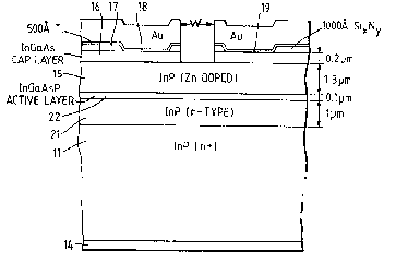
Referring to Figure 1, a twin stripe laser is facet
etched to produce two tw.in stripe lasers 1 and 2 on a
single chip. The 'parent' laser is a 1.3 um InGaAsP
double heterostructure laser grown on an InP substrate 11
using conventional liquid phase epitaxy.
1 309766
-- 5 --
The structure of the lasers is best dPscribed with
reference to Figures l and 2. The InP substrate ll is 100
- 150 um thick and is metallised on its lowermost face
14. Onto the substrate 11 are grown, by conventional
epitaxial growth techniques, four layers: a l um layer 21
of n-doped InP; a 0.1 um active layer 22 of InGaAsP
lattice matched to InP; a 1.3 um layer 15 of Zn doped InP;
and a 0.2 um capping layer 16 of InGaAs. Each of the
doped layers is doped to a conventional level for use in
semiconductor laser technology. The active layer 22 lies
between two layers 21, 15 Of higher band gap and lower
refractive index material to give both optical and carrier
confinement in a direction normal to the layers.
Onto the capping layer 16 is deposited a l000A layer
17 of Six~y. Two stripe windows 18, 19 are etched
through the SiXNy down to the level of the capping layer
16. A double metal layer of 3 um of Au on 500 Angstroms
of Ti is deposited on the dielectric layer 17 and into the
stripe windows 18, l9 then etched to form the four
contacts 12, 121, 13, 131 by forming the transverse
and longitudinal gaps H and W. Although both the Ti and
Au layers are etched to form the transverse gap H, only
the Au layer is etched to form the longitudinal gap.
Where the transverse gap H is formed the Au:Ti contact
layer is removed by ion beam milling, the silicon nitride
by dry etching with CF4, and the semiconductor layers
removed by reactive ion etching. Finally, the two current
stripes are electrically isolated by etching, using a
reactive ion beam, down to the bottom of the InGaAs cap
layer 16. As the reactive ion etch is not selective, the
etch step is stopped after a predetermined time calculated
with a knowledge of the etch rate. A slight over etch,
which removes part of the Zn doped layer, is acceptable.
1 309766
-- 6 --
The overall length (the distance between the end
facets3 of the device shown in Figure 1 is 325 um, with a
15 um wide facet etch displaced from the centre producing
asymmetrical devices with two pairs of waveguides 170 WQ and
140 um long. The overall width of the device is 200 um.
The stripe windows are 6 um wide, the inside edges of the
stripes being separated by 10 um.
The resistance measured between each pair of contacts
in a direction across the width of the device is about 40 Q
lo while that measured in a direction along the device,
traversing the transverse gap H, is greater than 200 K.~.
Operated one at a time, the four lasers exhibit similar
performance. With the dimensions and construction given
above, and with drive current pulses of 300 ns width, the
individual lasers typically have threshold currents of
around 140 mA above which TE polarised light was
generated. If the drive current is further increased, the
lasers begin to generate significant levels of TM light.
The increase in TM mode intensity is accompanied by a
rapid increase in the quantum efficiency of the lasing TE
mode, and a subsequent decrease in the intensity of the TE
mode.
When a pair of guides at one end of the device, for
example guides 1 and 2, are driven together with currents
above the threshold value of each individual laser guide,
the other pair of guides not being energised, there is
observed an abrupt, discontinuous decrease in the TE
intensity and sudden appearance of the TN mode in both
lasers. With equal drive levels of 170 mA to each of
Guides 1 and 2, strong polarisation switching is found as
shown in Figure 3. Here, a large and sharp decrease in
the intensity of one mode coincides with a similar
increase in the orthogonal mode. This switching occurs
1 30q766
- 7 ~
simultaneously in both guide outputs, in the same
direction. It is possible, by adjusting each current, to
achieve a virtual switch-off of the higher intensity
(lasing) mode with rejection ratios of the order of 20:1.
The switch can also be triggered in both directions by
superimposing brief, low amplitude current pulses onto one
of the drive currents. With the-300 ns drive currents
used,reliable switching could be achieved by superimposing
alternating positive and negative 10 ns, 5 mA current
lo pulses onto one of the drive currents. The operation was
independent of the adjacent device.
With the configuration shown in Figures 1 and 2 it is
also possible to switch the output of guides 1 and 2
optically by utilising the pair of guides 3 and 4, at the
opposite end of the device. With the Guides 1 and 2
energised with individual drive currents of 170 mA, a
short, 40 ns, threshold current pulse applied to one o~
guides 3 and 4 switched the output of guides 1 and 2 in
one direction. 100 r,s later a second similar current
pulse applied to the other guide (4 or 3) switched the
outputs of Lasers 1 and 2 back to the original state, as
shown in Figures--4a-4c.
The difference in level of the two triggering pulses,
sho~n in Figure 4cljl is due to the differerlce in threshold
values of the two guides 3 and 4 in the sample on which
Figures 4a-4c is based. With switching induced optically in
this way rejection ratios of more than 15:1 have been
obtained with a measured switching time of 100 ps, limited
by the rise time of the avalanche photodiodes of the
detection system. Such rapid switching makes the device
attractive for use in fast optical switches. The
combination of one of the devices and an optical polariser
1 309766
8 -
would enable very rapid on/off switching of laser light,
at a rate much faster than it is conventionally possible
to switch a semiconductor laser.
~y using a device of the general type shown in Figure
2, in combination with an appropriate polariser, rapid
on/off switching of a laser beam is effected using only
very small control currents at low voltage. It is clearly
an advantage of the present invention that switching can
be achieved without the necessity to use the high voltages
o required by electro-optic modulators and pockel~s cells.
Clearly, as those skilled in the art will understand,
there is no necessity for the source of the optical
triggering pulses (the triggering source) to be located on
the same chip as the laser whose output polarisation is
switched (the switching element). The optical triggering
pulses could be carried to the switching element by an
optical fibre or other optical waveguide. It is of course
also not essential that the triggering source comprises
lasers which are essentially identical to those of the
switching element. Hence, although the wavelength of the
triggering pulses should be within the gain spectrum of
the switching element (which typically would be a few tens
of nanometers), it is possible for the triggering source
to comprise a laser of a configuration other than
twin-stripe or twin-ridge and of materials other than
InGaAsP alloys. The triggering source could also consist
of a single laser, rather than what is effectively two, by
providing some means to switch its output between the two
guides of the switching element. When using optical
triggering pulses, the polarisation of the triggering
pulse is that to which the appropriate waveguide output is
to be switched.
1 3()9766
When the device i6 used in the current-controlled
switching mode, the triggering sourc~ which is not
activated, appears to make no contribution to the
operation of the device. Consequently it appears that one
half of the device shown in Pigure 2, that is either
guides 1 and 2 or guides 3 and 4, could be produced
separately and used as a current controlled polarisation
switch. Such a device has the advantage that it is very
small and provides controlled polarisation switching
1 without the need for extra components such as gratings.
A large number of devices of various different
dimensions and combinations of dimensions have been
fabricated and assessed and have been found to give the
desired rapid controlled switching of polarisation states.
This polarisation switching characteristic makes
devices according to the invention use~ul in optical logic
applications. Firstly, the devices can provide an
inverting function by showing a low output when addressed
by an external optical signal. This operation iS shown in
Figures 5a-5d, where a TE polarised optical input pulse 40
from a source produces a corre~ponding dip 42 in the TM
o~tput, Figure 5c, of device 43. Simultaneously, the TE
output, Figure 5b, of device 43 shows the opposite
reaction, a positive pulse corresponding to the TN
"negative pulse". Overall, the total light output,
Figure 5d, of device 43 stays substantially constant in
accordance with the profile of the current pulse I2
applied to the relevant electrode of device 43. The
current supplied to the two electrodes of the switching
element is such, in this example, for the device to
operate in a switchable mode rather than in a bistable
mode. It is for this reason that the optical output
switches back to TN after removal of the TE input pulse.
~2
1 309766
- 10 -
For this mode of operation, the current applied to the
electrode should be somewhere in the range where, were
both electrodes to be driven, there is a rapid decrease in
TE output, and a simultaneous increase in TM output, with
increasing current (as previously described with reference
to Figure 3). In general, the requisite current for this
type of operation will be somewhere within the range of
1.1 to 1.4 times threshold current, the actual operable
range of any device generally being narrower than the just
quoted range. For the device used to generate Figure 3, a
current of slightly less than 170mA would be appropriate
( 1.2 x It). It is, however, an easy matter to
determine the appropriate electrode current, since the
TE/TN transition is readily observed. 0f course, if the
switching element were initially to have a TE output, the
input pulse would need to be TM polarised if the switching
element's output polarisation were to be switched. This
type of action could be used to provide an optical ~NOT~
gate.
Secondly, this inverting function can be used in an
optical logic clock, as shown schematically in Figure 6.
Here the device 25 without the triggering source is placed
in an external cavity 26 which incorporates a quarter wave
plate 27 which enables light emitted with TE polarisation
to be reinjected as TN and vice versa. The result is
switching of the laser output between the orthogonal
polarisations at the round trip period of the cavity. The
external cavity 26 comprises a mirror 28 and a facet 29 of
the device 25. Alternatively, a second distinct mirror (not shown)
may effectively take the place of the facet as the
cavity's second reflector. In either configuration, the
near facet 31 of device 25 is preferably anti~reflection
coated but this is not essential. In the first
1 30q76h
configuration the ~istant facet 29 (in this embodiment a
cleaved facet) is not anti-reflection coated, and hence
functions as a mirror, while in the second configuration
it too is preferably anti~reflection coated. When
mirror 28 is planar, an objective lens 32 is used between
the near facet 31 and the mirror 28. As shown in Figure 6
the objective lens is positioned between the quarter-wave
plate 27 and the laser 25. With an external cavity length
of about 30cm we have achieved stable operation of a clock
lo of this type over several hundred cycles. The device was
operated in the bistable mode with both electrodes
receiving similar currents.
In order to achieve the desirable effects that we have
observed a sufficient level of coupling between the
waveguides is required. Those skilled in the art will
appreciate that the amount of coupling between two
waveguides which are ad~acent and substantially paralleI one
with the other is dependant on the product of the length
of the waveguides and the coupling coefficient. As those
; 20 skilled in the art will also be aware, the coupling
coefficient is dependant on the width and separation of
the waveguides, and on the index difference between each
guide and its surroundings. While we believe that it may
be possible to provide too much coupling, we have not yet
managed to produce a structure which, as the result of too
much coupling, fails to achieve the desirable effects we
are seeking. The following ranges of dimensions, taken
together with the other information contained within this
specification should enable those skilled in the art to
produce devices according to the invention but using
different materials, (eg GaAlAs - GaAs), dimensions and
configurations.
1 309766
- 12 -
We have found that the length of the switching device
is important, as is the separation of the waveguides in
that device. stripe separation has been varied over a
range from s~m to more than 20~m. Above 20~m separation,
with the configuration and waveguide lengths that we are
using, there tends to be insufficient coupling between the
waveguides for sharp triggering to be achieved. If the
length of the switching device waveguides is less than
about 170~m, rapid bistable switching between polarisation
o states is no longer achieved although the output
polarisation state is still in fact switchable optically
or by controlling the drive current. Switching is
achieved within about 3 ns, this being limited by the
carrier recombination time. Preferably the switching
device has a cavity length o~ more than 170~m, more
preferably more than l90~m.
Stripe width was varied in the range 5 to 6~m but
within this range was found to have no effect on the
polarisation switching characteristic.
Devices of the type shown in Figure 2 were also made
with a range of different gap widths between the
triggering element and the switching element. Gap widths
ranged from 15 to 20~m and within this range this variable
2~ was found to have no effect on the polarisation switching.
Given that the switching ele~ent is essentially based
on the presence of a pair of suitably coupled waveguides
it is worth looking at what other structures could be used
to provide such an optical confiquration.
Although the laser devices descri~ed above use
standard stripe geometries, both gain and index guiding is
involved in the device operation. Consequently it is not
essential that simple stripe device structures be used.
Suitable alternative waveguide structures include ridge or
p
1 309766
- 13 -
buried heterostructures as these can allow ready TE/TM
operation. Clearly the tighter optical confinement
provided in index guided structures means that in general
the two guides, if there is to be sufficient coupling
between them, will have to be closer together than the
corresponding guides in gain guided structures such as
those described above. Depending on the length of the
cavities, and other factors, the waveguides should
preferably be no more that about 15~m apart, and more
preferably no more than about lO~m apart. The minimum
cavity length needed to achieve sufficient interaction and
coupling is generally likely to be appreciably more than
150~m and may be more than 200~m.
We have found that with devices as described above the
desirable effects are obtained without the need for any
control of device temperature. Not only is this a
tremendous advantage, but it is also very unexpected,
since others unsuccessfully looking to achieve controlled
polarisation bistability have assumed that precise
temperature control would be necessary.