Note: Descriptions are shown in the official language in which they were submitted.
13~7~1
01 This invention relates to switching
02 devices and in particular to an MOS FET switch array
03 Which conSumeS considerably reduced silicon substrate
04 area than prior art devices.
05 Analog crosspoint switches which connect
06 an array of ir,puts to an array of ou'pu~s are
07 typically fabricated as separate MOS FET transis~ors
08 in a silicon substrate. Each separate transistor is
09 isolated from the others, and to connect n inputs to m
outputs of the array, a total of n x m transis~ors are
11 necessary to be used to form the switching array. In
12 order to reduce resistance through the array when the
13 transistors are on, the transistors are generally
14 produced having large features. The result is that
considerable area of an integrated circuit is used in
16 the formation of the array, which is costly and
17 reduces the product yield.
18 The present invention is a structure for
19 producing an array, described in two embodiments,
which considerably reduces the area of silicOn
21 substrate surface used, to provide the same number of
22 cross-points as in the prior art. Whereas using the
23 separate switching transistor array structure, the
24 number of impurity diffused regions is 2 x n x m, in
one embodiment this is reduced to 3/2 x n x m, and in
26 the other embodiment the number of diffusions is
27 reduced to (n x m)/2 ~ 1. Since each impurity
28 diffused region involves the use of a certain area of
29 the silicon substrate, it may be seen that in the
latter embodiment the substrate surface area required
31 for the diffused regions is reduced to approximately
32 1/4 or less than for the prior art single transistor
33 structure. Considerably reduced cost and increased
34 yield clearly results.
The improvements are obtained in a
36 semiconductor crosspoint apparatus having a plurality
37 of inputs for connection to a plurality of outputs via
38 - 1 -
.. ' ~
13 ~ ~ a~ ~ ~
01 field effect transistor (FET) switches, each FET being
02 comprised of a pair of impurity diffused regions in a
V3 silicon substrate each usable as a source or as a
04 drain and being separated by a channel region having
05 an insulated gate thereover. A pair of diffused
06 regions for a pair of FETs are common and form a
07 central single dif~used re~ion, separated by channel
08 regions for the respective FETs on both sides of the
09 single diffused region from separate diffused regions
of the pair of FETs. The single diffused region can
11 be connected to one output and the separate diffused
12 regions can be connected to corresponding separate
13 inputs to allow switching connections of eithe -
14 both of the separate inputs to the one output by
application of a switching signal to one or both of
16 the insulated gates.
17 According to another embodiment successive
18 ones of a group of single diffused regions are
19 connected to different outputs and one of each of the
separate diffused regions of FETs of the group are
21 connected together to one input and the other of the
22 separate diffused regions of the group are connected
23 together to another input, whereby said one and
24 another inputs can be separately switched by the FETs
to ones of the different outputs.
26 According to a preferred embodiment, pairs
27 of the separate diffused regions of different FETs
28 which are connected to the same input are common,
29 forming separate single diffused regions. Preferably
the separate single diffused regions and the central
31 single diffused regions alternate continuously in a
32 row, separated by the channel regions forming the
33 various transistors. The result is a continuous row
34 of transistors having common diffused regions, except
for the transistors at the end of the row, which have
36 their outer diffused regions not in common with any
37 other.
38 - 2 -
1 3 ~
1 In accordance with an embodiment of the invention,
2 a semiconductor crosspoint switch apparatus has a plurality
3 of separate inputs for connection to a plurality of separate
4 outputs via a row of similar polarity type field effect
S transistor (FET) switches, each FET being comprised of a pair
6 of separate impurity diffused regions in a silicon substrate
7 each useable as a source or as a drain and being separated by
8 a channel region having an insulated gate thereover, each
g pair of ~ETs having a diffused region in common which common
diffused region is not in common with any other FET, each
11 common diffused region forming a central single diffused
12 region separated by channel regions for the respective FETs
13 from remaining separate diffused regions of the pair of FETs,
14 the single diffused region being individually connected to
one output and the remaining separate diffused regions being
16 individually connected to corresponding separate inputs
17 whereby switching connection of either or both of the
18 separate inputs to the one output is effected by application
19 of a switching signal to one or both of the insulated gates.
In accordance with another embodiment, a
21 semiconductor crosspoint switch for switching each of a
22 plurality of first terminals of a matrix of terminals to a
23 plurality of second terminals of the matrix of terminals, is
24 comprised of an integrated circuit comprised of a series of
field effect transistors (FETs) of similar conductivity type
26 each formed of a pair of impurity diffused regions separated
27 by a channel region underlying an insulated gate, pairs of
28 FETs sharing adjacent diffused regions, the number of
29 diffused regions being equal to twice the number of the
larger number of the first and second terminals plus one,
31 each terminal of the larger number of the input and output
32 terminals being respectively connected in sequence to a
33 corresponding even numbered diffused region, a pair of the
34 smaller number of the first and second terminals each
3s connected to alternate odd numbered diffused regions
36 respectively, and apparatus for applying a switching signal
37 to at least one gate whereby an FET having the gate can
38 conduct, thereby connecting a first terminal and a second
39 terminal connected to the FET together.
- 2a -
13 ~ ~ ri ~1
01 It should be understood that the inputs
02 and outputs car, be reversed, and referer-ce in this
o3 specification to arl input should alternatively be
04 construed as reference to an output, and vice versa.
05 A better understanding of the invention
06 will be obtained by reference to the detailed
07 descriptior, below, in conjunction with the following
08 drawings, in which:
o9 Figure 1 illustrates a cross-point switch
array,
11 Figure 2 is a plan view of a typical
12 layout of transistors in a silicon substrate without
13 its metallization layer according to the prior art,
14 Figure 3 is a cross-section of a single
FET switch according to the prior art of the kind used
16 in Figure 1,
17 Figure 4, is a plan view of a group of
18 transistor structures forming an array in accordance
19 with a first embodiment of the invention,
Figure 5 is a cross-section of one of the
21 transistor structures shown in Figure 4,
22 Figure 6, is a plan view of the preferred
23 form of the invention, and
24 Figure 7 is a cross-sectional view of part
of the array of Figure 6.
26 Turning now to Figure 1, a schematic view
27 of a cross-point switch array is shown. Each of the
28 inpu~s in the column X, that is, X0,XlXn is to be
29 connected to each of the outputs of the column Y,
30 being Y0,YlYm. The connections are provided by
31 means of switches 2. The switches are typically
32 fabricated as individual MOS FET transistors (herein
33 referred to as FETs).
34 Figure 2 illustrates an array of switching
transistors 2. Reference is also made to Figure 3
36 - 3 -
~3~7g~
01 illustraLir,g a cross-section of one of the
02 transistors. The transistor is shown without its
03 usual conductor metal1ization layer to make the
04 invention clearer.
oS Each FET is formed of an impurity diffused
06 region 3 forming a source or drain separated by a
07 channel region 4 from another impurity diffused region
08 5 forming a drain or ~ource. The sources, drains and
o9 channels are contained within a silicon subs~rate 6 in
a well known manner.
11 Above the channel region is an insulating
12 layer 7, typically formed of silicon dioxide.
13 conductive gate layer 8, typically formed of
14 polycrystalline silicon overlies the insulation layer
7.
16 As is well known in the art, application
17 of an appropriate voltage at a gate terminal 9 allows
18 signals applied to the source or drain region 3 from
19 an input terminal 10 to pass via the channel region 4
to output terminal 11.
21 Individual switching transistors of the
22 type described above are connected between each input
23 X0-Xn and each output X0-Xm, forming the switching
24 array or matrix.
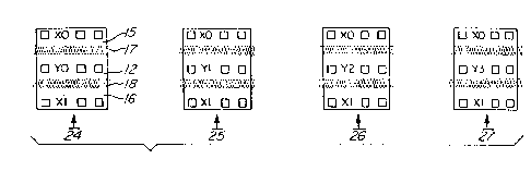
; 25 In accordance with a first embodiment of
26 this invention as shown in Figures 4 and 5, a pair of
i 27 impurity diffused source or drain regions of a pair of
28 FETs connected between a pair of inputs, e.g. X0 and
29 Xl and a single output, e.g. Y0 are common, forming a
central single diffused region 12. The central single
31 diffused region 12 is separated by channel regions 13
32 and 14 for the respective FETs on both sides of the
33 single diffused region from separate diffused regions
34 15 and 16 of the pair of FETs. Thus common impurity
diffused region 12 forms a source or drain and regions
36 15 and 16 form drains or sources for two transistors
37 with common region 12. Gates 17 and 18 are insulated
38 - 4 -
:`' f,~ `
13 (~ ~ r~
01 via insulatin~ dielectri~s 19 and 20 respectively from
02 channel regions 13 and 14. For the device shown ir,
03 Figure 5, two inputs 21 and 22 are connected by the
04 two FÆTs thus formed to output terminal 23.
OS It may be seen that the two transistors
06 24A and 24s in Figure 2 having input regions marked X0
o7 and Xl and outputs marked YO have a final
08 metallization layer deposited thereover in order to
o9 form the switching matrix, and as a result the two
outputs YO are connected together. In the present
lI invention (Fig. 4) a similar function is achieved by
12 merging (making comrnon) the diffused regions of the
13 two transistors, to provide a single output which
14 in this example would be connected to output Y0.
Four such double transistors each forming
16 two crosspoints are shown in Figure 4, as
17 representative examples. It may be seen that as
18 marked the two inputs of each multiple transistor are
19 connected to the inputs X0 and Xl, while the outputs
are connected to different output terminals Y0, Yl,
21 Y2~ Y3, etc. In the example shown in Figure 4, a
22 2 X 4 matrix is formed, but it will be obvious to a
23 person skilled in the art that larger arrays can be
24 set up in similar fashion. Clearly, also inputs and
outputs are interchangeable.
26 In this construction, it may be seen that
27 there is a saving of space on the silicon chip which
28 would be required to form a diffused region for one of
29 each of the transistors, as well as ~he area required
for isolation regions around each of those
31 transistors. Rather than requiring 2 x n x m source
32 and drain diffusions, as with the embodiment shown in
33 Figures 4 and 5, only (n x m) x 3/2 diffused regions
34 are required to provide the same number of crosspoints
as in the prior art.
36 Figures 6 and 7 show a layout and a
37 cross-section of a silicon chip according to a
38 - 5 -
3 ~
01 preferred embodimen~ of the invention. In this case
02 pairs of the separate diffused regions of the
03 diferent FETs shown in Figure 4 which are connected
04 to the same input are common, formir-g separate single
05 diffused regions. It is thus preferred that the
06 separate single diffused regions and the central
07 single diffused regions alternate continuously in a
08 row separated by the channel regions, as shown in
o9 Figure 6.
To understand the structure of the device
11 of Figure 6, it would be illustrative to consider
12 first Figure 4. If one connects each of the
13 transistors of Figure 4 in series, by placing the
14 bottom two diffused regions of transistors 24 and 25
which are connected as marked to input Xl together in
16 common, and place the top two diffused regions of
17 transistors 25 and 26 both of which are connected to
18 input X0 in common, and place the bottom two diffused
19 regions connected to input Xl of transistors 26 and 27
together in common, the structure resulting ir, Figure
21 6 is obtained. The designations X0-Xn indicate the
22 connections of the diffused regions to the various
23 correspondingly labelled inputs and the designations
24 Y0-Yn indicate their connections to the
correspondingly labelled outputs. At one end is a
26 not-common source or drain single diffused region 15
27 for connection to input X0, then the common diffused
28 region 12 for two transistors as described above for
29 connection to output Y0, then a common diffused region
28 which would form the other of the drain and source
31 of transistors 24 and 25, if separated, for connection
32 to input Xl, then a common diffused region 29
33 corresponding to common diffused region 12, but in
34 transistor 25, for connection to output Yl, then the
common diffused region 30 of the regions which would
36 be transistors 25 and 26 in Figure 4 which would be
37 connected to input X0, etc., each separated by
38 - 6 -
~ 3 ~ J ~1
01 channel regions and gates 18, 18A... 18n. At the end
02 of the array is a single not-common source or drain
03 di~fused regiori 31 of the end transistor.
04 A cross-section of the above is shown in
05 Figure 7 which is dire~tly analogous to Figure 5, but
06 a sequence of separate si~gle diffused regions and
o7 central single diffused regions alternate in a row.
08 separated by the channel regions.
o9 The embodimer,~ of Figure 7 has a further
reduced number of diffused regions from the embodiment
11 of Figures 4 and 5, being (n x m)/2 + 1.
12 As may be seen in Figure 7, diffused
13 region 15 is connected to input terminal 21 which can
14 be connected to input X0, diffused region 12 is
connected ~o output terminal 23 which can be connected
16 to output Y0, diffused region 28 can be connected to
17 input X1 via input terminal 32, diffused region 29 can
18 be connected to output Y1 via output terminal 33,
19 diffused region 30 can be connected to input X0 via
input terminal 34, etc.
21 In the above-described manner large
22 cross-point switch arrays can be formed. With this
23 embodiment the amount of silicon surface area required
24 for the diffused regions is approximately 1/4 or less
than that required in the prior art structure shown in
26 Figure 2. Significant economy and increase in product
27 yield results, without increasing the resistance per
28 cross-point, for devices with similar feature sizes as
29 in the prior art.
A person understanding this invention may
31 now conceive of alternative embodiments or variations
32 thereof using the principles described herein. A11
33 are considered to be within the sphere and scope of
34 the invention as defined in the claims appended
hereto.
36 - 7 -