Note: Descriptions are shown in the official language in which they were submitted.
1310052
~ 54,366
CIRCUIT FOR CONTROLLING POWER DISSIPAT~D
B~ AN ~LECTRICAL RESISTANCE
BACRGROUND 0~ THE INVENTION
The present invention relates to a
circuit for controlling ths power dissipated by
an electrical resistance and particularly to a
circuit which does not require an RMS to DC
converter.
Electrical resistance heaters are used
in a variety of environments. While control of
the power dissipated by the electrical
rosistance heater is not always critical, in
certain environments, it is critical that the
power dissipated by the electrical resistance
hoater be controlled 80 that it does not vary by
more than a small percentage.
, An example of one type of environment
in which the control of the power dissipated by
an electrical resistance heater is critical is
in a split ther~owell in a water induction
monitoring system. A water induction monitoring
'~
13100~2
-2- 54,366
system may be used in a power plant to check for
water in the steam lines of a steam turbine.
The water induction monitorinq system typically
includes a plurality of split thermowells which
are positioned in the steam lines.
FIG. 1 is a schematic cross-sectional
view of an example of a split thermowell 20
which is employed in a water induction
monitoring system. Referring to FIG. 1, the
split thermowell 20 is mounted in a steam line
or pipe 22 and extends approximately 8 inches
into the steam pipe. The split thermowell 20
includes a casing 24 having a U-shaped portion
26. Mounted within the casing 24 are an
electrical resistance heater 28 and
thermocouples 30 and 32. The resistance heater
28 is coupled to a power supply 29 and is used
to heat the thermocouples 30 and 32 which in
turn provide sensing siqnals Tl and T2,
respectively, to a central control circuit (not
shown). As long as there is no water between
the legs Or the U-shaped portion 26 of ths
ca~ing 34, th- dirrerence between the two
temperature signals T1 and T2 output by the
thermocouples 30 and 32 should be relatively
high ~on the order Or 10- to 200-F). However,
ir the dir~erence between the temperature
signal~ Tl and T2 drops to less than lO-F, then
thi~ i~ an indication that there is water
between the legs of the U-shaped portion 26, due
to the ract that water has a thermoconductivity
which is greater than that ror steam. When this
drop in the dir~erence in temperature i9
.
~.
- 131~i,0~
_3_ 54,366
detected, the water induction monitoring system
wlll issue an alarm
In order for the split thermowell 20
to function properly, it is necessary that the
power of the electrical resistance heater 28 be
regulated The power dissipated by the
resistance heater 28 is given by the following
equation
p 8 IRMS2 X RH (l)
where IRMS i~ the RMS current flowing through
the heater 28 and RH iR the resistance value of
the re~istance heater 28 There are typically
variations in the supply voltage which is
provided to the resistance heater 28 Since the
, resistance value of the resistance heater 28
does not chanqe, such variation~ in the supply
voltag- will result in variatlons in the current
(IRMg) ~lowing th~rough the resistance heater 28,
~ with r-~ultlng variation~ in th- power (P)
dis~ipat-d by th- el-ctrical r-sistance heator
28 Thu-, the pow r will t-nd to vary unle~s
th- RMS current Or th- re~istanc- heater 28 i9
r-gulat-d The pow-r di~slpatlon in the
r~ tanc- h-ater 28 ln a pllt thermowell 20 is
controllabl- to bo ~rom 5 to 6S watts based on
lt~ po-itlon in the system Typically, the RMS
curr-nt through the re~i~tance heater i~
controlled to keep th- power disslpated
con~tant
The RMS current o~ an l-ctrical
r~ tanc- h-at-r ~or pulsed current wave~orms
:
, . .
: -:
,
- ~.
~310~
~4~ 54,366
~e g , see FIG 2) i8 given by the following
equation
IRMS ' Ipeak ~ ~ (2)
Thus, in order to maintain the RMS current
constant, it i~ necessary to ad~u~t th~ duty
cycle (ton~T~ with variations in the peak
current
FIG 2 is a waveform diagram
illustrating the duty cycle ~or the current
wave~or~ o~ the current flowlng through the
resistance heater 28 Thus, the RMS heater
current (IRMS) must be regulated becauss the
peak current will change wlth line voltags
variatlons which may vary by-as much as ~ 10
Ir it i~ as~umed that the reslstance valu- o~
the he~t-r 28 ~tay- the sam-, then in ord-r to
hav- th- pow-r maintained con-tant, th- ON tim-
o~ th- current which flow- through th-
r~ tance heater 28 must b- controlled For
xa~plo, th~ hlgher th- curront, the more OFF
ti~- that i~ r-quir-d In th- prior art, a
awitching typ- regulator utilizing pul~e width
modulation or phase control 1- commonly used ~or
heat-r current control to produce a pulsed
heater current wave~orm o~ the type illustrated
in FIG
As indicated above, there are a number
of circuits employing electrical resistance
heater~ ~or which control o~ the power
disslpated by the electrical re~istance heater
i~ de~lrable An example o~ ono circuit which
ha- been employed in the prior art to control
s,"' ,~
~~ 13100~2
-5- 54,366
the power dissipated by an electrical resistance
heater is illustrated in the block diagram of
FIG 3 of the drawings In FIG 3, an
electrical resistance heater 34 has a resistance
RH and is coupled to a supply voltage VBus
While the resistance RH will tend to remain
constant, there will typically be variations in
the supply voltage VBus A sensing resistor 36
has a resistance Rs and is employed to sense the
current flowing through the resistance heater
34 An RMS to DC converter 38 including a
squaring circuit 40, an averaging filter 42 and
a square root circuit 44, squares the voltage
across the sensing resistor 36, averages the
squared voltage and takes the square root of the
average, to provide a voltage signal which is
proportional to the RMS current flowing through
the resistance heater 34 This ~eedback voltage
i9 then subtracted rrom a voltage corresponding
to th- RMS current reference value by a
subtractor 46 to provide a current error signal
Th- current error signal is amplified by an
intogrator 48 which provides the high steady
stat- loop gain required ~or precise regulation
Th- ampli~ied current error signal is applied to
a pul~- width modulator 50 which generate~ the
reguired duty cycle ~or driving a switching
d-vice 52 such as a MOSFET, bipolar transistor,
etc When the switching device 52 is ON,
current ~lows through the resistance heater 34
Th- current which ~low~ through the heater 34 is
det-rmined by the supply voltage
VBUs and the resistance values RH, Rs and tho
re~l~tance o~ the switching device 52
- '
-` 1310~2
-6- 54,366
since the supply voltage VBus is
unregulated it will tend to vary with the AC
supply voltage by + 10% The RMS to DC
converter 38 is required because of this DC
supply voltage variation Without the RMS to DC
converter 38, the control circuit would act to
regulate the average heater current rather than
the RMS heater current As a result, the heater
power dissipation would vary by the same
percentage as the DC bus voltage variation
(i e , + 10%) if the average heater current is
maintained constant By employing the RMS to DC
converter 38, the RMS current is controlled to
within ~ lS with line voltage variations of
~ 10% While RMS to DC converters are available
as monolithic integrated circuits, accurate
laser trimmed version~ o~ the~- converters are
very expensive, and lower cost versions require ?
unde~irable external trimming Further, in
~yst-m~ with a large number Or electrica~
r-Jl-tane- heater~, it ls neces~ary to provide
~uch a h$gh co~t RMS to DC convorter for each
l-etrical r~ tanc- heat-r ~'or xample, in
th- wat-r induction monitoring system describ-d
abov-, th~re may be a~ many a~ rifty thermowells
20, and thu~ rirty electrical resistance heaters
28 in the monitoring system Therofore, each
l-etrical resistance heater 28 will require an
exp-n~ive RMS to DC converter to control the
power dissipated by the electrical resistance
heat-r 28
Thore i~ a need in the art for a low
co~t circuit ~or accurately controlling the
. , ~
,~ . , .
, ..... ' : .
- ' ..
'
.
-` 13~0~2
-7- 54,366
power dissipated by an electrical resistance
heater.
S _ Y OF ~E INVENTION
The present invention is directed to a
circuit for controlling the power dissipated by
an electrical resistance which overcomes the
deficiencies of the prior art.
In particular, the present invention
is directed to providing a circuit for
controlling the power dissipated by an
electrical resistance and particularly an
electrical resistance heater, which does not
employ an RMS to DC converter~
The circuit for controlling the power
di sipated by an electric resistance in
accordance with the present invention includes
means, coupled to the electrical resistance, for
providing a feedback current corresponding to a
current flowing through the electrical
resistance. The circuit further includes means
~or providing a correction current corresponding
to variations in the supply voltage, and means
~or receiving the correction current and the
~eedback current, for ampli~ying the error
indicated by the correction current and the
feedback current, and for controlling the ~low
of current through the electrical resistance to
control the power dissipated by the electrical
resistance. In the preferred embodiment, the
electrical resistance is an electrical
resistance heater, and the circuit of the
invention is u~ed to maintain the power
1 3 ~ 2
-8- 54,366
dissipated by the electrical resistance heater
constant
In the control circuit of the present
invention, the means for providing the
correction current includes means for providing
a variable current corresponding to variations
in the supply voltage, means for providing an
RMS reference current and means for providing an
additional reference current The RMS reference
current, the variable current and the additional
reference current are combined to produce the
correetion current whieh is eombined with the
feedbaek current In one embodiment, the mean9
for providing the additional re~erenee eurrent
eomprises a Zener diode and a resistor
In another embodiment, the means for
providing the additional re~erenee eurrent is
seleeted to have values so that the means for
providing the RMS referenee current can be
removed from the cireuit
The~e together with other ob~eets and
advantag-~ whieh will beeome ~ubsequently
apparent, re~id- in th- details of eonstruetion
and op-ration a~ more fully hereinafter
2S d-~erlb-d and elaimed, referene- being had to
- th- aeeompanying drawings forming a part hereof,
wher-in lik- numerals refer to like parts
throughout
~EI~y_r~SCRIPTION OF THF DRAWqNGS
FIG 1 is a sehematie eross-seetional
vi-w of a ~plit th-rmowell having an eleetrieal
re-i-tanee h-ater;
' ~' ,
,'' '~ ~ ' ' ', : '
' ~
.
.
.
~ 13100a2
_9_ 54,366
FIG. 2 is a waveform diagram for
illustrating the duty cycle of a current
waveform for current flowing through an
electrical resistance heater;
FIG. 3 ig a block diagram of a prior
art control circuit for controlling the power
dissipated by an electrical re~istance heater;
FIG. 4 is a graph of the normalized
average current required in order for the RMS
lo current ~lowing through an electrical resistance
heater to remain constant, versus the normalized
DC supply voltages which varies by + 10%;
FIG. 5 is a graph of a percentage
power error versus the normalized supply voltage
i~ the average current i9 determined by the
straight line approximation of the curve in
FIG. 4;
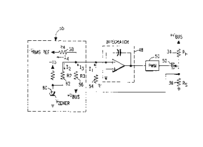
FIG. 6 is a circuit diagram of a
circuit for controlling the power dissipated by
an electrical resistance in accordance with a
first embodiment of the present invention; and
FIG. 7 is a circuit diagram of a
clrcuit for controlling the power dissipated by
an eloctrical resistance in accordance with a
~econd embodiment o~ the present invention.
DETAILED DFSCRIPTION O~ THE PREFERR~D ~MBODIMeNTS
The present invention is based on the
diw overy by applicant that for pulsed current
wavefor~s such as that shown in FIG. 2, in order
for the ~MS current to remain constant as the DC
supply voltage changes, the average current
through the resistanco heater must change in
accordance with the following eguation:
-10- 54,366
avg (VBUS) = Iavg (vnOm) V
VBus
where Iavg (VBUS) is the average heater current
at the supply voltage Vgus, Iavg (Vnom) is the
average heater current at the nominal bus
voltage (i.e., Iavg (VnOm) = Ipeak x ton/T) and
VnOm equals the nominal bus voltage. Thus, V
equals the assigned or nominal value of the
voltage, while VBUs equals the actual value of
the supply voltage which may vary by + 10% from
the nominal value.
FIG. 4 is a graph of the normalized
average current required in order for the RMS
current to remain constant, versus the
normalized supply voltage which varies by + 10%.
The dashed curve A in FIG. 4 illustrates the
average currents which must be provided for the
variations in the supply voltage which are
indicated. That is, the dashed curve A shows
what the average current must be in order to
maintain a constant power dissipation. The
solid lino B in FIG. 4 is a straight line or
linear approximation of the dashed curve A.
FIG. 5 is a graph o~ the percentage
power error versus the normalized bus voltage.
Line C illustrates the percentage power error if
the average current remains constant, while
curve D shows the percentage power error if the
average current through the resistance heater is
varied in accordance with the ~traight line
approximation B o~ FIG. 4. As is clear ~rom
curve D, the power error is at most -1% when the
supply voltage is at the maximum and minimum
-
~ ~ - ~
~ 3 ~
-11- 54,366
ends of its range of variation. Thus, it is
clear that the straight line approximation for
variations in the average current, which is
illustrated by line ~ in FIG. 4, can be employed
to control the average current so as to
effectively control the power dissipated by the
resistance heater. In fact, the percentage
power error i~ as low as that provided by more
expensive prior art RMs to DC converters.
FIG. 6 ig a circuit for implementing
the linear changes in average current with
variations in bus voltage, as illustrated by
solid line B in FIG. 4. Referring to FIG. 6, in
accordance with the rirst embodiment of the
present invention, instead of feeding back a
signal proportional to the RMS current flowing
through the resistance heater 34, a correction
current is produced by a correction circuit 55
based on variations in the ~upply voltage. The
correction circuit 55 is a means for providing a
correction current, and includes a resistor 56
which is coupled to the supply voltage VBUs to
produce a variable current I3 which varies with
variationJ in the ~upply voltage VBus. Thus,
re~istor 56 form~ a means ~or providing a
variable current. A resistor 58 having a
re~istance value R4 is coupled to an RMS
r-~erence voltage (-VRMs REP) in order to
produce an RMS re~erence current I4. A
reference Zener diode 60 and a resistor 62
having a resistance value R2 ~orm a means for
providinq an additional re~-ronce current I2.
Re~istor 36 and a resistor 54 having a
re~istance value Rl form a means for providing a
310~
-12- 54,366
feedback current Il corresponding to the eurrent
through the resistance heater 34.
In the preferred embodiment, the Zener
diode 60 is a precision voltage reference Zener
diode which is used to generate the addition31
reference current I2 which i8 a constant
current. The value R2 f the resistor 62 is
selected so that the additional reference
current I2 i~ equal to the value of the variable
current I3 when the supply voltage VBUs is at
its nominal value. If the DC supply voltage
(VBus~ is below its nominal value, then variable
current I3 will be lower in ~agnitude than
additional reference current I2. As a result,
the average heater current Iavg (and thus the
feedback current Il), will be increased since
the control loop will act to maintain Il + I3 -
I2 ~ I4 at steady state. If the DC supply
voltage i8 above the nominal value, then I3 will
be greater in magnitude than I2, thereby causing
tho hoater average current Iavg (and therefore
the ~eedback current Il) to decrease. The RMS
re~erence current I4 acts to control the duty
cycle whon the supply voltage is at its nominal
lev-l, since the duty cycle will be ad~usted
through closed loop control until the average
value o~ I4.
The RMS heater current at the nominal
bùs voltage is provided by equation (2) where
the peak current Ipeak is equal to the nominal
bus voltage divided by RH + RS + the resistance
o~ switching element 52. ~he values o~ the
circuit para~eters are selected as follows. ~he
pr-ci~lon voltago of th- Z-n-r dlod- 60 1Y
1.~
. :
:
" 13100~2
-13- 54,366
initially selected Then, Rl, R2, R3 and R4 are
selected to have values such that the following
equations are satisfied
R2 = R3 Vzener
VnOm
R3 - Rl Vnom
VS
Vrms ref ~ VS (6)
R4 Rl
where Vs equals the average value of the voltage
acro~s resistor 36 at the nominal bus voltage
and at the desired RMS heater current
As illustrated by the embodiment of
FIG 7, the circuit of the present invention can
be simpli~ied since I2 and I4 are always
con~tant I~ R2 i9 s-lected to have a value
egual to the voltage o~ the Zener diode 60
divid-d by ~I2 + I4) th-n resistor 58 can b-
~ inat-d ~rom the correction circuit 80 that a
modl~i-d correction circuit 55' re~ult~ ~see
PIG 7), because the voltage o~ the Zener diode
60 i~ u~ed a~ the oole reference
Re~erring back to FIG 6, slnce the
variabl- current I3 i~ a DC current, while the
~--dback current Il is a puls- current, the
integrator 48 i~ u~-d to ~ilt-r out the pul-ing
and provide A DC level output I~ the ~eedback
current Il increases due to an increa~e in the
. .
., ,
.: ,
1 3 1 ~ O j 2
-14- 54,366
supply voltage, then the pulse width of the
pulso width modulator 50 is controlled to
decrease If the feedback current Il decreases
due to a decrease in the supply voltage, then
the pulse width output of the pulse width
modulator 50 i8 controll~d to increase
Together, the integrator 48 and the pulse width
modulator 50 form a means for reeeiving the
eorr-etion current and the ~eedbac~ current, for
amplify$ng the error indieated by the correetion
eurrent and the feedbaek current, and for
eontrolling the flow o~ eurrent through the
re-istanee heater 34 to eontrol the power
dl~sipat-d by the resistane- heater 34 In the
pr-~-rr-d embodiment, the flow o~ eurr-nt
through th- resistanc- heater 34 i~ controll-d
to maintain the power dissipat-d by the
r~ tan¢e heater 34 constant Furth-r, as
illu-trat-d by th- circuit~ o~ FIGS~ 6 and 7,
th- pr-sent invention is directed to a h-at-r
~or~ d by th- l-ctrieal r-~istanee heater 34
and m-an~ ~or eontrolling th- average eurr nt
, ~lowlng through th- h-at-r 34 to ~ati~y
quation (3) (1 - , th- eireuitry oth-r than
2S r~ tane- h-at-r 34)
Th- eireult ~or eontrolling pow~r
dl~-lpat~d by an ~leetrieal r-sistanee in
aeeordane- with the present inv~ntion is
advantag-ou~ in that it provide- pow r control
withln -1% ov-r a ~ 10% variation in supply
voltag- by mploylng a v-ry impl-, low co~t
~ ~ eireult whleh do-~ not employ an RMS to DC
;~ eonv-rt-r Thu~, th- elreult o~ th pr-~-nt
~ ~ inv-ntlon provlde- power eontrol whieh
' "I ' ' '
~-
, ,
iL31~2
-15- 54,366
essentially corresponds to that provided by a
circuit including an RMS to DC converter,
without the incumbent complexity and expense
which is associated with such an RMS to DC
converter circuit. Tha circuit of the present
invention for controlling the power dissipated
by an electrical resistance may be implemented
in numerous ways. For example, while the
precision reference voltage iY described as
lo being provided by a Zener diode 60, any other
suitable type of reference voltage supply may be
employed. While a specific embodiment of a
correction circuit for providing a correction
current corresponding to variations in the
supply voltage has been illustrated in FIGS. 6
and 7, any other circuit which is capable of
providing such a correction current may be
employed. Further, while the preferred
embodiment has been described with respect to an
electrical resis~.ance heater, the present
invention may be employed to control the
power dissipated by any type Or electrical
resi~tance.
The many feature~ and advantages of
the lnvention are apparent from the detailed
~pe¢l~ication and thu~ lt is intended by the
appended claim~ to cover all such feature~ and
advantages of the ~ystem which fall within the
true ~pirit and scope o~ the invention.
Further, since numerous modifications and
change~ will readily occur to tho~e skilled in
the art, it i9 not desired to limit the
invention to the exact construction and
operation shown and described and, accordingly,
-16- 54,366
all suitable modifications and equivalents may
be resorted to, falling within the scope of the
invention.
,
';;~' ~, ' .
~,
,
:
';
;~:
''~,~' '~ ' '
,~,, : :
"
. ,
,,