Note: Descriptions are shown in the official language in which they were submitted.
131(3~' 1
10577-1a,2/T9
TWO- STAGE SYNCHRO~I I ZER
BACKGROUND OF THE I NVENT I ON
The present invention is directed generally
to digital equipment, and more particularly to appara-
tus for synchronizing transitions of an input signal to
a transition of a digital clock signal in the form o a
periodic pulse train within one period of the pulse
train.
In digital systems, it is not unusual to con-
trol the transfer of data between independent units,
such as a device controller and a peripheral device
controlled thereby, using control strobe pulses or, as
they are more usually called, "handshake" signals.
Generally, a handshake signal will signify, for exam-
ple, that a piece of data is present on the input/out-
put lines connecting the peripheral device and its con-
troller. The handshake can then be applied, along witha timing or clock signal (usually in the form of a pe-
riodic pulse train) to appropriate logic to effect proper
data transfer (or other operations). In such circum-
stances, synchronization is desired, if not necessary,
between the handshake and a clock to avoid generation
of spurious signals. --
Often, due to physical tolerances in the man-
ufacture of the hardware used to control such systems,
the relative position in time of the handshake signal
and clock will vary over a range, even if the devices
are driven in lock-step by a common clock. Such varia-
tions in the duration and timing of handshake signals
cause problems where the handshake must be present in
synchronism for the handshake to be recognized as valid.
More often, however, units that communicate
with one another are synchronously operated by their
r
2 1 3 1 07 1 1
own independen-t clocks so that -the handshake signals
between them appear asynchronously.
Further, because of the nature of presently
known synchronizing circuits, synchronization cannot be
achieved in less time -than one clock period - even in a
best case situation. However, in high-speed data trans-
fers between, for example, a peripheral device and its
corresponding controller, it is often necessary that
data transfers occur in a time period that is no more
than a clock period in order to prevent data overrun
(i.e., incoming data overriding immediately preceding
data). Data overrun problems can be cured by one of
two methods: Adding more logic circuitry in the form
of additional buffering (and multiplexing the incoming
line to the separate buffers), or ensuring that the
ultimate transfer of a first piece of incominq data is
made before the immediately succeeding piece of data is
~ost (i.e., slow down the transfer rate). The former
method adds expense and complexity to the system, the
latter costs time.
SUMMARY OF THE INVENTION
Accordingly, the present invention provides,
in a minimum of circuitry, apparatus for synchronizing
an incoming signal to transitions of a periodic pulse
train.
Broadly, the invention comprises the method ~-
of sampling and storing the input signal at each tran-
sition (i.e., each change of state) of the periodic
pulse train with which the input signal is to be syn-
chronized; producing from the sampled step a first sig-
nal that is indicative of the stored state of the input
signal, sampling and storing the first signal at each
transition of the periodic pulse train; and producing
from the stored first signal a representation of the
input signal that is synchronized with the periodic
pulse train.
131071 1
3 6~157-259
The invention disclosed i5 implemented by providing a
first pair of ~lip-flops each respectively configured to sample
and store the input signal on the positive and negative-yoing
transitions of the periodic pulse train in the form of a digital
clock signal (`'clcck"). The TRU~ (Q) outputs of the flip-flops
are connected to an OR gate, the ou~put of which is sampled and
stored at each clock transition by a second pair of flip-ilops.
The outputs of the second pair of flip-flops form synchroniz~d
versions of the input signal, having state transitions occurring
substantially with those o~ clock These output signals may be
logically ORed by an OR gate to form a signal that is synchronized
with both state changes of clock.
A number of advantages are achieved by the present
invention. First, in a minimum number of circult components, a
two-stage synchronizer is formed capable of synchronizing the
leading edge of an input signal to a transition of a clock
signal - within one period of the clock, maximum.
Aacording to a broad aspect of the invention there is
provided apparatus for synchronizing a transition between first
and second states of an input signal to positive or negative
transitions occurring in a periodic pulse train, the apparatus
aomprising:
first storage means coupled to receive the input signal for
sampling and storing ~he state of the input signal at each
positive transmission of the periodic pulse train;
second storage means coupled to receive the input signal for
sampling and storing the state of the input signal at each
3a 1 31 n71 1 6~lS7-25'~
negative transition of ihe peri.odic pulse train;
first circuit means operable to produce a first signal
indicative of the state of the input slgnal stored in the first or
second storage means; and
second circuit means operable in response to t.he first signal
and the pulse train to produce a representation of the input
signal having first and second state transitions synchronized with
the transitions of the pulse train, the second circuit means
including third storage means coupled to sample and store the
first signal at each positive transition of the periodic pulse
train, and fourth ætorage means coupled to sample and store the
first signal at each negative transition of the periodic pulse
train.
According to another broad aspect of the invention there
is provided a method of synchronizing changes of state of an input
signal to positive or negative transitions of a periodic pulse
train, the method comprising the steps of:
sampling and storing the state of the input signal at each
transition of the periodic pulse train;
producing a first signal indicative of the stored state of
the input signal;
sampling and storing the first signal at each transition of
the periodic signal, and producing therefrom first and second
representations of the input signal with changes of state
occurring at each of the transitions of the periodic pulse train;
and
0 7 1 1
64157-~59
3b
receiving the first and second representations ~o produce
therefrom an output signal that is representatlve of ~he input
signal t the outpu~ signal having changes of sta~e occurrlng at the
positive or negative transit.ion of ~he periodic pulse train.
The above and other advantages and features of the
present invention will become readily apparent to one skilled in
the art upon reading the following detailed description of the
invention, which should be taken in conjunctlon with the
accompanying drawlngs.
BRIEF DESCRIPTION OF THE DRAWI~GS
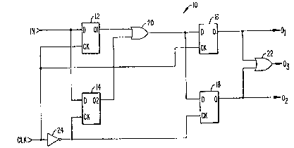
Figure 1 is a circuit diagram of a two-stage
synchronizer constructed in accordance with the teachings of the
present inven~ion disclosed herein; and
Figure 2 is a timing diagram, illustra~ing opera~ion of
the two-stage synchronizer of Figure 1.
DETAILED DESCRIPTION OF TH~ INVE~TIO~
Referring first to Figure 1, there is illustrated a two-
~tage synchronizer, constructed in
~ ~ c~ ~
4 l ~l O Ill
accordance with the teachings of the present invention
and designated generally with the reference numeral 10.
As constructed, the two-state synchronizer 10 operates
to synchronize the transitions or state changes of an
input signal (IN) to the transitions of a periodic pulse
train in the form of a clock (CLK) signal. As Fig. 1
shows, the two-stage synchronizer 10 includes four D
type flip-flops 12, 14, 16 and 18; a pair of OR gates
20 and 22, and an INVERT~R 24. The IN signal, an aper-
iodic, asynchronously-appearing pulse, is coupled to
the data (D) inputs of the flip-flops 12 and 14, while
the CLK signal is coupled to the clock (CK) inputs of
the flip~flops 12 and 16, and to the input of the IN-
VERTER 24. The output of the I~V~RTER 24 is coupled to
the clock (CK) inputs of the flip-flops 14 and 18.
Thus, while the CK inputs of the flip-flops 12 and 14
receive the "true" version of the CLK signal, the CK
inputs of the flip-flops 14 and 18 receive the inverted
or phase-shifted (by 180) version of the CLK signal.
The flip-flops are of the type that sample
and store the state of the signal then appearing at the
D input on the rising or positive-going edge of the
signal applied to the CK input. Flip-flop 12, there-
fore, samples the IN signal on positive-going transi-
tions of the CLK signal while the flip-flop 14 samples
the IN signal on the negative-going transitions of CLK. --
To put it another way, the pair of flip-flops 12, 14 -
operate to sample and store the state of the IN signal
at each transition of the CLK signal.
The outputs (Ql and Q2, respectively) of the
flip-flops 12 and 14 are coupled to an OR gate 20 that,
in turn, produces a first signal that is communicated
to the data (D) inputs of the flip-flops 16 and 18.
Similar to the pair of flip-flops 12, 14, the flip-flops
16 and 18 also respectively operate to sample and store
the state of the first signal on each positive and
negative-going transition of the CLK signal.
' ' ' (f ~(
l 3 ~ 07
The outputs (Q) of the pair of flip-flops 16,
18 form the output signals l and 2 produced by the
two-state synchronizer lO. II1 addition, the o outputs
of the flip-flops 16, 18 are coupled to the inputs of
the OR gate 22 to produce a third signal, 03. All three
output signals l~ 2' 3 each form a synchronized rep-
resentation of the IM signal.
Referring now to Eiy. 2, a timing diagram is
shown to illustrate operation of the two-stage synchro-
nizer 10 in which the CLK signal (waveform 30) is usedto periodically sample the state of the IN signal (wave-
form 32) to produce synchronized representations in the
form of the signals l~ 2 and O3 (waveforms 38, 40 and
42).
The CLIC signal (waveform 30), as Fig. 2 il-
lustrates, is shown as having a 50% d~ty cycle, although
that is not necessary to the present invention, and
positive and negative-going transition between upper
and lower logic states (or voltage levels) 54 and 56,
respectively.
In operation, assume that prior to the time
period Tl (Fig. 2) the IN signal is at a lower or first
state, and that during the time period Tl, the IN signal
traverses to the higher or second assumable state. The
time period Tl is intended to indicate that period of
time, relative to the rising edge 50 of the CLK signal, --
during which the flip-flops 12, 14 are "blind" to state
changes of the IN signal; that is, state changes from a
lower to a higher level of the IM signal occ-lrring in
the time period Tl will not be seen, and the flip-flop
12 will, at the rising edge 50 of the CLK signal, store
a LO~.
However, at the immediately succeeding, or
negative, transition of the CLK signal the IM signal
has had time to set up to the HIGH state and, there-
fore, that HIGH will be stored in the flip-flop 14 on
the negative transition of CLK - at time T2. The HIGH
6 ~ J ~ ~ I
at the Q2 output of flip-flop 14 is communicated via
the OR gate 20 to the data (D) inputs of the flip-flops
16 and 18 so that, at the next succeeding CLK transi-
tion, which in the example here will be posi-tive-going,
the flip-flop 16 will sample and store, in effect, the
content of the flip-flops 12, 14, causing the output Q3
to go HIGH at time T3. In turn, via the OR gate 22,
the output signal 03 (waveform 42) will also go HIGH.
Thus, all three output signals l~ 2 and 03 form a
representation of the IN signal that is synchronized to
the transitions of the CLK signal. A similar analysis
can be made for the falling or negative-going transi-
tion of the IN signal.
Continuing with reference to Fig. 2, at time
period T4 another leading (positive) transition of the
IN signal occurs around or shortly after a negative
transition 52 of the CLK signal. Again, the transition
of the IN signal is not seen by the flip-flops 12, 14
because of its closeness to the transition of the CLK
signal. However, at the immediately succeeding transi-
tion of the CLK signal (time TS) the IN signal has set-
tled and, since this transition will be positive, the
flip-flop 12 will sample and store the now HIGH state
of the IN signal. Thereafter, at time T6 (the next
succeeding negative transition 52 of the CLK signal)
the output Q4 from the flip-flop 18, and therefore the -
output signals l and 03 go HIGH (waveforms 38 and 42). --
Again, the output signals l and 03 form a representa-
tion of the IM signal that is synchronized to the ris-
ing or positive transition of the CLK signal.
One may ask what is the need for the second
rank of flip-flops 16, 18. It will be noted that, in
Fig. 2, synchronization appears to be achieved by the
output of the OR gate 20. The answer is found in the
metastability of flip-flops. If a transition of the IN
signal occurs at exactly (or very close to exactly) the
transition of the CL~ si~nal, the outpu-t of the flip-
r~ ~(
7 1 31 (~7 1 1
flops 12, 14 will be indeterminate. In fact, the out-
puts can oscillate between a "one" and a "zero" state
for a limited time. This situation is unacceptable.
The second rank of flip-flops 16, 18 prevents this os-
cillation from propagating through to the rest of thecircuit.
In summary, there has been disclosed a syn-
chronizer circuit for synchronizing an inpu-t siynal to
a clock signal formed from a periodic pulse train.