Note: Descriptions are shown in the official language in which they were submitted.
131~3Q9
COMW:155
HIGH SPEED MICROPROCESSOR WITH
ONE-SHOT TIMER FOR 8-BIT I/O ACCESSES
This invention relates to apparatus for enabling a
relatively high-speed microcomputer system which includes
both an 8- and a 16-bit system bus to utilize in a more ef-
fective manner slower-speed input~output (I/O) devices in
conjunction with the 8-bit bus.
The timing of the operations of the various components
in a microcomputer system must be suitably matched, as is
well known to those of ordinary skill in the art of design-
ing and building such systems. An oversimplified analogy
is a conventional automobile engine. The various engine
components' operations must be properly synchronized so
that eàch cylinder receives its fuel-air mixture in turn, a
spark is generated within that cylinder to ignite the mix-
ture, and the piston delivers its power stroke, all in a
smooth sequence.
Likewise, the synchronization of a microcomputer sys-
tem requires attention by the system designer(s). A prin-
cipal need for proper timing arises in connection with the
exchange of signals between the various system components.
131~
For example, as those of ordinary skill are aware,
components such as the central processing unit (CPU), sys-
tem memory, I/O devices (e.g., disk drives, printers, user
terminals, and the like), and other such components typic-
ally communicate with each other by "broadcasting" signals
on one or more signal buses. (As used in the art, the term
"bus" generally means an electrical connection resembling a
telephone party line in some respects, to which a number of
signal-gnerating and -processing components are connected.)
Each such signal broadcast on a "party line" in this
manner by a component is typically coded with an identifier
designating the other component which is the intended re-
cipient of the signal. A component connected to a given
signal bus in effect "listens" electrically to that bus for
signals encoded with the component's designator. The iden-
tifier for a given component is often referred to as the
component's address on the signal bus, although strictly
speaking the component can usually be physically attached
to the bus at any convenient location.
As an example, the CPU might perform a write-to-memory
operation by broadcasting a signal encoded with the desig-
nator for the memory device to be written to and the actual
datum to be written. A11 memory devices would "hear" the
signal, but one in particular would recognize its own des-
ignator and save the accompanying datum in its electronic
storage circuits. In like manner, the CPU might later
perform a read-from-memory operation by signalling the
memory device to send a return signal back to the CPU, the
return signal being encoded by the memory device with the
previously stored datum.
Many microcomputer systems have been designed using
; A the relatively slow Intel 8086/8088 family of microproces-
sors, frequently in accordance with the industry standard
r~e- nn~r~
13~ 3~9
--3--
exempli~ied by various Compaq computers manufactured and
distributed by the assignee of this application. The
8088 CPU commonly operates at a speed of 4.77 MHz, and
computer systems based on the 8088 or 8086 CPU ordinarily
have an 8-bit system bus.
(The bit size of a system bus refers to the "width" of
the bus's electrrical data path. An 8-bit bus allows eight
separate electrical signals, each representing either a 1
or a 0 depending on whether the voltage is on or off, to be
transmitted simultaneously; it is roughly analogous to an
8-lane highway. Generally speaking, a 16-bit bus can han-
dle higher-volume information flows than can an 8-bit bus.)
Later designs of CPUs in that family, such as various
versions of the Intel 80386 can operate at speeds of 12
MHz, 16 MHz, or 20 MHz. (MHz i5 an abbreviation for mega-
Herz, or millions of cycles per second.) Computers based
on these later CPUs typically include both an 8-bit and a
16-bit system bus in order to maintain compatability with
older system designs.
A number of I/O devices and other peripheral devices
were originally designed for a relatively slow microcom-
puter system having an 8-bit system bus. Such devices
needed only enough speed to keep up with the relatively
slow CPUs of that time. Speed limitations associated with
the devices generally did not cause bottlenecks with re-
spect to CPU speeds. For example, software which ordered
the CPU to direct two write operations in succession to the
same device usually posed no difficulty: the CPU's speed
in executing the software instructions was not fast enough
to cause a problem.
Use of such 8-bit devices with a faster CPU can lead
to synchronization problems. In the class of microcomputer
systems exemplified by the Compaq Deskpro 286, for example,
using the Intel 80286 CPU, it was found that the CPU was
able, in some instances, to go fast enough to exceed some
of these I/O device limitations. This is roughly analogous
to a person giving dictation over the telephone party line
to another person who transcribes it: the transcriber may
be able to handle a relatively slow talker satisfactorily,
but cannot keep up with a fast talker. In the same manner,
an older I/O device, designed for a slower CPU, may not be
able to keep up with a faster CPU.
In the past, this problem has been alleviated by chan-
ging the applications software which controlled the CPU to
ensure that I/O signals generated by the CPU under the con-
trol of the software did not outrun the devices in ques-
tion. In software for the Deskpro 286-class products, for
example, this was typically done by inserting additional
instructions (such a3 JMP instructions) between the offend-
ing I/O operations. With a JMP instruction in particular,
the CPU was forced to discard the contents of its prefetch
queue and refetch the next instruction. This took signi-
ficant time (one to two microseconds) and provided adequate
delay in between the I/O cycles.
This is not a desirable general solution, however.
Additional delay would need to be built into the software
to prevent a faster, 80386 CPU from outrunning the I/O
device. The software in question would consequently run
that much slower on a slower CPU. This problem can be al-
leviated by having multiple versions of each software pro-
gram, but the attendant maintenance burdens make software
vendors normally reluctant to do so. In addition, a change
to one area of a program might result in unexpected bugs in
other areas.
72159-17
The outrunning problem would be particularly exacerbated
in an 80386 CPU which utilized a posted-write memory cache system
such as the ~Intel 82385. In a posted-write cache system, the CPU
treats a write operation as ended when its interaction with the
cache controller is ended; the cache controller actually completes
the write operation. Numerous JMP instructions would be required
to prevent outrunning in such an environment.
Hardware-based solutions can include disabling or
stopping the system bus after 8-bit I/0 cycles, or after all I/0
cycles (both 8- and 16- bit), by means of additional wait states
or hold cycles. In systems based on the *Intel 80386 CPU,
operating-system software can be designed to trap I/0 cycles and
artiflcially add the reguired delay Either option, of course,
leads to a corre~ponding cost ln processing time.
In accordance with the preferred embodiment of the
present lnvention, there is provided logic circuitry to identify
the end of each 8-bit I/0 cycle; a timer to time out a 1.5
microsecond timeout after the end of each such cycle; and the
logic circuitry, which if the timer has not signalled the end of
the timeout when a subse~uent I/0 cycle begins, adds wait states
to the I/0 cycle until the timeout has expired.
In accordance with the present invention, there is
provided a method of synchronizing operations of a computer system
including a central processing unit (CPU), input/output (I/0)
access decode circuitry, a timer operationally connected to the
CPU and the access decode circuitry, and uti].izing one or more
input/output (I/0) devices which include at least one 8-bit
*Trade-mark
`:
6 72159-17
input/output (I/0) device, comprising the steps of: upon an
attempt by the CPU to access an 8-bit I/0 device, the access
decode circuitry starting the timer to generate a timeout for 1.5
microseconds, without generating wait states associated with said
attempt; and upon a subsequent attempt by the CPU to access an I/0
device prior to expiration of the timeout, the timer signalling
the CPU to insert wait states to delay the subsequent I/0 access
until the timeout period has expired.
The invention will now be described in greater detail
with reference to the accompanying drawings, in which figure 1 is
a state-machine diagram describing logic circuitry for
implementing the invention; and
Figure 2 is an illustration of the component
configuration of the present invention.
Referring to figure 1, the initial state of the logic
circuitry is idle, as represented by a state circle 1. Following
an 8-bit I/0 access, indicated by the event arrow 2, a timer is
started as indicated by state circle 3.
When the timer times out, as indicated by the event
arrow 4, the logic returns to its idle state. If a second I~0
access ~8-bit or otherwise) is initiated prior to the timeout, as
indicated by event arrow 5, wait states are added to delay the I/0
cycle until the timer times out.
The timer does not stop the processor until and unless
another I/0 access is attempted. Thus, memory operations (as
distinct from I~0 operations~ can continue as normal during the
timer period as long as a second I/0 access does not take place
R
7 13~ la~
72159-17
during that time. Only an 8-bit I/O cycle starts the timeout,
but any type of I/O cycle that follows will be held up until
the timeout expires.
It has been found that a timeout of 1.5 microseconds
will produce satisfactory results for nearly all 8-bit I/O
devices not utilizing their own timing control mechanisms (e.g.,
handshaking or other such signals). A longer timeout will of
course suffice, but unnecessary delays are of course undesirable.
A shorter timeout may produce satisfactory results for some
devices, but a timeout of 1.0 microseconds is likely to be
insufficient for at least some 8-bit I/O devices.
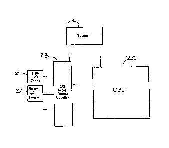
Referring to Figure 2, a preferred embodiment of the
present invention is illustrated comprising a CPU 20 connected
to two I/O devices 21, 22 via I/O access decode (logic)
circuitry 23. One of the I/O devices is an 8-bit device 21
while the second I/O device 22 can be of any size. Coupled to
the I/O access decode circuitry 23 and the CPU 20 is a timer 24.
This apparatus is to operate according to the state-machine logic
defined in Figure 1. Thus, when the CPU 20 completes an access
to the 8-bit I/O device 21, the I/O access decode circuitry 23
initiates the timer 24 having a timeout period of 1.5 micro-
seconds. If the CPU 20 then attempts to access the second I/O
device 22, or even the 8-bit device 21 again, prior to expiration
of the timeout period, the timer 24 signals the CPU 20 to insert
wait states into the I/O access cycle delaying access until the
timeout period expires.
It will be appreciated by those skilled in the art
having the benefit of this disclosure that this invention as
,~
8 1~113~
72159-17
claimed below is believed to be capable of application in other
situations. Accordingly, this description is to be construed as
iLlustrative only and as for the purpose of teaching those
skilled in the art the manner of carrying out the invention.
It is also to be understood that various modifications
and changes may be made without departing from the spirit and
scope of the invention as set forth below in the claims. It is
intended that the following claims be interpreted to embrace all
such modifications and changes.