Note: Descriptions are shown in the official language in which they were submitted.
~31i3~3 61293-184
RELATED APPLICATIONS
This application is related to the following
applications which are in the name of Digital Equipment
Corporation. These applications contain, at least in part, common
disclosure regarding an embodiment of a peripheral repeater box.
Each, however, contains claims to a different invention: Canadian
patent application S.N. 574,576 filed on August 12, 1988 for a
D.C. Power Monitor, Canadian patent application S.N. 574,585 filed
on August 12, 1988 for a System Permitting Peripheral
Interchangeability, and Canadian patent application S.N. 574,290
filed on August 10, 1988 for a Method of Packetizing Data.
BACKGROUND OF THE INVENTION
This invention relates to computer systems in general
and more particularly, to a peripheral repeater box for use in a
computer system to which a plurality of peripherals can be
connected.
In large computer systems, and particularly in systems
which provide graphics displays, a plurality of different types of
peripheral devices
A
3 ~ 3
for providing input to the computer system are
provided. For example, a single system may have as
inputs a keyboard, a mouse, a tablet, a light pen,
dial boxes, switch boxes a~d so forth. In a system
with a plurality of such peripherals it is
advantageous to have a device which can collect
inputs from each of these peripherals and then
retransmit the various inputs over a single line to
the computer system. Such a device is referred to
herein as a peripheral repeater box in that it acts
as a repeater for each of the individual
peripherals.
Very often, different peripherals have the
same type of plug. In typical systems of the prior
art there is a requirement that each peripheral be
plugged into a specific connection. If by mistake
two different peripherals which have the same type
of plug are mixed up, the inputs no longer react
properly. There is thus, a need for in a
peripheral repeater box the ability to plug
different type of peripherals into the same
connector and still be able to recognize which
peripheral is connected.
Various peripherals are capable of
operating at different baud rates. It i8 sometimes
necessary to change baud rates. In systems using a
peripheral repeater box, resetting of baud rates
must be done both in the peripheral and the
peripheral repeater box. There is thus, a need to
.
æi L 3
- 3 -
provide a system in which baud rates can be set,
such baud rates being automatically set both in the
peripheral itself and in the peripheral repeater
box.
Preferably, a peripheral repeater box of
this nature, which will include its own processor,
will be capable of running various levels of self
test. Some indication should be given of the
status of the peripheral repeater box, i.e. whether
it is in a test mode or in an operating mode. In
addition, since the peripheral repeater box will
require a number of different power supplies to
provide power to electronics therein, an indication
of the proper operation of these supplies is also
necessary.
Finally, there is a need to e~tablish data
protocols for the peripheral box to communicate
with the peripherals and with the computer system.
Ideally, such should be bo'h simple, trouble-free
and efficient.
MKaRy OF T~ INVENTION
The peripheral repeater box (PR box) of the
present invention provides all of the above noted
functions in addition to others.
:
13~3~ ~
61293-18~
The PR box of the present invention is, first of all,
used to allow the peripherals to be powered at the monitor site.
The PR box collects the various peripheral signals using, a
conventional RS-232-C or RS-423 connection, from seven peripheral
channels, which are then packetized and sent to a host, e.g. a
computer and/or graphics control processor, using RS-232-C
signals. Transmissions to the peripherals are handled in a like
manner from the host, i.e., receiving packets from the host,
unpacking the data and channeling data to an appropriate
peripheral serial line unit (SLU).
The peripheral repeater box of the present invention is
particularly suited for use in a graphics system of the type
disclosed in copending Application Serial No. 574,288, entitled
Console Emulation For A Graphics ~orkstation.
The communications between the PR box and host are
carried out with a novel protocol, which provides for reliable
error free transmission.
The PR box uses a system with circular queues and
buffers to buffer incoming and outgoing messages to and from the
peripherals. Messages are arranged in packets for transmission.
The
-- 4 --
~ A
.,
, .
.
4' 3
completion of a message from a peripheral is
detected by counting bytes. Alternatively if the
time between received bytes exceeds a predetermined
amount, this is used to sense the end of a message.
To keep communications active between the PR Box
and the system, a "keep alive" timer is used. This
causes a "keep aliven message to be sent if there
has been no other communication within a
predetermined amount of time.
In addition to providing a
multiplexing/data concentration function for the
peripherals, the PR box also implements a self-test
check on its own logic (performed on power-up and
on command request) and an external loopback
function for manufacturing testing. The
manufacturing test mode, which is an extended
version of self-test, operates when the
manufacturing jumper is detected in circuit. When
in this mode the self-tests run continuously unless
an error is detected at which time it will loop on
the failing test. This mode requires a special
loopback module.
A function LED and a group of 8 diagnostic
LEDs are located on the back panel of the PR Box.
The function LED is utilized to indicate which
state the PR box is in, i.e., the function being
performed. The current error status, if any, is
reflected in the diagnostic LEDs. The diagnostic
LEDs are also available to the host to provide
additional status information in the case where the
graphics system is unable to display messages on
its video display. A command is available to the
system by which to write an error code to the
diagnostic display. In accordance with the present
invention, the function LED is a tricolor LED
permitting indication of one of three states of
conditions of operation.
A DC power monitor is included to monitor
the power supply and indicates power status with a
bicolor LED. This monitor provides a rough
indication of positive and negative 12 volt power
supplies. If either supply is out of spec 10 to 15
percent then the LED will indicate a failure by
changing its color. The DC power monitor is itself
powered by a 5 volt supply. If the LED is out,
this indicates failure of the 5 volt supply.
Peripherals which are supported by the
disclosed embodiment of the PR Box include:
a keyboard;
a mouse;
a tablet; and
a dial box.
In addition, in the illustrated embodiment,
three other channels are provided for future
expansion to provide for a button box channel, a
spare keyboard channel and a general spare RS-232-C
channel.
~31~31~
61293-184
The PR box of the present invention permits
in~erchangeability of the different peripherals. In other words,
peripherals with the same type plug can be plugged into any of the
peripherals ports and it is not necessary to ensure that a
particular peripheral is plugged into a particular port. On
power-up and each time a peripheral is plugged in or removed, the
host checks the peripherals to determine what type of device it is
and keeps track of that information.
A further feature of the present invention is the
ability to change baud rates for those devices which support
different baud rates. In accordance with the present invention, a
command from the host to change baud rates automatically resets
the baud rate of the receiver in the peripheral box for the
particular channel and another command sets the baud rate of the
peripheral itself. First, a message is sent through the PR box to
the peripheral. Then a command is sent to the PR box to change
the baud rate of a UART (Universal Asynchronous
Receiver/Transmitter) associated with that peripheral.
The first broad aspect of the present invention defines
in a system which includes a data transmitting device; a repeater;
and a data receiving device, the repeater accumulating input data
in packets from said transmitting device and retransmitting said
packets to said receiving device, a memory structure for storing
said data in said repeater comprising: (a) a data buffer; (b) a
receive queue having a plurality of entries, each entry capable of
storing a starting address for the packets in said data buffer
received from said transmitting device; (c) a transmit queue for
~3~3~3
61293-18~
storing the starting addresses of packets for transmitting to said
receiving device; and (d) means to transfer said addresses from
said receive queue to said transmit queue, each of said buffer and
said queues being circular.
The second broad aspect of the present invention defines
in a system which includes a data transmitting device; a repeater;
and a data receiving device, a method of communication between the
data transmitting device and the data receiving device comprising:
(a) accumulating input data from said transmitting device at said
repeater in a data buffer; (b) entering into a receive queue
having a plurality of entries, a starting address for the packets
in said data buffer received from said transmitting device; (c)
transferring said addresses from said receive queue to a transmit
queue for storing the starting addresses of packets for
transmitting to said receiving device; each of said buffer and
said queues being circular and ~d) retransmitting said packets to
said receiving device.
The third broad aspect of the present invention defines
a method of operating a memory device having a finite total amount
: 20 of physical memory space in connection with at least one operating
.:
device and a central processing unit comprising the steps of: (a)
allocating a preselected amount of said finite total amount of
physical memory space, with a beginning and an end, for said at
least one operating device; (b) selectively transmitting data from
said at least one operating device to said central processing
unit; (c) operating said central processing unit to transfer said
transmitted data from said at least one operating device to within
- 7a -
.
61293-184
sa:id preselected amount of physical memory space allocated for
sa:id at least one operating device until said central processing
unit reaches the end of said preselected amount of physical memory
space; (d) upon reaching the end of said preselected amount of
physical memory space, further operating said central processing
unit to continue to transfer said transmitted data, by
transferring said transmitted data to the beginning of said
preselected amount of physical memory space without interrupting
transfer of said transmitted data, whereby causing said
en~
preselected amount of physical memory space a~d to be connected to
the beginning thereby causing said preselected amount of physical
memory space to be circular.
- 7b -
A
~31 ~ 3i~
BRIBF DE8CRIPTION OF THF DRAWING8
Fig. 1 is a block diagram of a computer
system in which the PR box of the present invention
may be used.
Fig. 2 is a basic-block diagram of the PR
box of the present invention.
Fig. 3 is a schematic diagram of the DC
power monitor of the present invention.
Fig. 4 is a schematic diagram of the
function indicator LED of the present invention.
Figs. 5A-C are a flow diagram of the
firmware running in the PR box of the present
invention.
Figs. 6A-H illustrate the transmission of
packets through the use of circular queues and
circular buffers according to the present
invention.
- 9 -
Fig. 7 is a table tabulating the default
baud rates for the different peripherals used in
the preferred embodiment of the present invention.
Fig. 8 is a table showing the character
times associated with each baud rate for use in
interpacket timing according to the present
invention.
Fig. 9~ iS a flow diagram illustrating the
basic timing utilized for interpacket timing.
Fig. 10 is a diagram showing the
configuration of the header byte field utilized
with the present invention.
Figs. llA-C are diagrams showing the
message transmission protocol of the present
invention.
Fig. 12 is a chart illustrating various
states of the function LED and the diagnostic LEDs.
~::
~ 3 ~ ~ 3 13 6l293-l84
DETAILED DESCRIPTION
Svstem Overview
Fig. 1 is a block diagram of a computer system showing
where the peripheral repeater box of the present invention fits
into the system. The illustrated system is a graphics system.
However, the present invention is applicable to other computer
systems. Thus, there is illustrated a monitor 11 which receives
video input from a RGB coax 13 which is coupled to computing
apparatus 14 which does the graphic computations. Included in
apparatus 14, as illustrated, is a graphics engine or graphics
processor 15, a main computer 17, e.g. a *Vax 8250 system, and a
computer 19 acting as a control processor, which may be a
*Microvax computer. Computer 17 is host to computer 19 and
computer 19 is host to the PR box 21 described below. Thus,
hereinafter, where reference is made to a host, the reference is
to computer 19. The operation of this part of the system is more
fully described in Application Serial No. 574,288, entitled
Console Emulation For A Graphics Workstation. The peripheral
repeater box 21 is illustrated in Fig. 1 along with the various
peripherals which may be plugged into it. These include a
keyboard 23, a
*Trademark
,
-- 10 --
A
1 3 ~ 3
11 --
mouse 25, a tablet 27, knobs 29, i.e. a dial box,
buttons 31, a spare RS232 channel 33 and a spare
keyboard input 35.
The peripheral repeater box is a self-
contained microprocessor system which, in the
illustrated embodiment, is located underneath the
monitor. It is responsible for handling
information flowing between the host and peripheral
devices. This is a free running sub-system that
performs a self-check of its own internal status at
power up. After completing this task it
initializes itself and continuously scans for
activity from the host or peripherals.
~ our peripheral channels (~or keyboard 23,
mouse 25, tablet 27 and knobs 29) and one command
channel ~for communications with the host) are
provided to connect all the supported peripherals.
In addition three spare channels for future
expansion or special peripherals, e.g. the spare
keyboard 35, button box 31, and spare 33 of Fig. 1
have been provided.
The sub-system is composed of a minimal
system as shown in Fig. 2. Thus, there is
illustrated an 8031 microprocessor CPU 41 which, in
conventional fashion, has a associated with it a
clock/reset unit 43 with a 12 mHz cyrstal
oscillator. Coupled to the ~031 CPU is a
oonvention~l control decode block 45 which couples
' .
~31~ 3~i ~
the CPU to a bus 47. BuS 47 couples the CPU to
memory 49 which includes 16K of RAM 51 and 8K of
ROM 53. The 8031 has no on chip ROM and
insufficient on chip RAM. For this reason, the
8031 is used in an expanded bus configuration
utilizing three of the four available general
purpose ports for address, data and control. These
are coupled through block 45 to bus 47. Enabling
the external addressing capability for the expanded
bus configuration is accomplished by grounding
(through a jumper) the EA, external access, pin.
~ he low order address and data are
multiplexed on the 8031, the address is latched
during addres~ time with a 74LS373 Octal latch
strobed via the ALE ~address latch enable) signal
output from the 8031.
Bus 47 is also connected to a diagnostic
register 55. Diagnostic register provides an
output to a display 57 comprising 8 LEDs. Also
coupled to bus 47 is a function register 59 which
provides its output to a tricolor LED 61 to be
described in more detail below. Also shown in Fig.
2 is the DC power monitor 63 which provides its
output to a bicolor LED 64 to indicate under or
over voltage conditions as explained in detail
below.
1 3
Bus 47 also connects to Serial Line Units
(SLU) 0-7 along with a modem control contained in
block 62. Block 62 is what is known as an octal
asynchronous receiver/tra~smitter or OCTALART.
Such a device is manufactured by Digital Equipment
Corporation of Maynard, MA. as a DC 349.
Basically, the OCTALART comprises eight identical
communication channels (eight UARTS, in effect) and
two registers which provide summary information on
the collective modem control signals and the
interrupting channel definition for interrupts.
Serial line units 0-6 are coupled to the seven
peripherals indicated in Fig. 1. SW 7 is the host
link shown in Pig. 1. The outputs of the SLUs are
coupled through tran~ceivers 69, the outputs of
which in turn are connected to a distribution panel
71 into which the variou~ connectors are plugged.
Block 69 includes ElA Line drivers, 9636 type,
operating off a bipolar supply of +/-12 volts which
translate the signals from TTL levels to a bipolar
RS-232-C compatible signal level of approximately
+/- 10 volts.
The host channel (S W 7), keyboard channel
and spare channel do not have device detection
capability. The other five channels have an input
line that is connected to the DCD (Data Carrier
Detect) pin of the corresponding SLU of the
OCTALA~T 62. When the pin is at the channel
.
.
~3~3 ~ 3
connector side is grounded the input side of the
OCTALART is high indicating that a device is
present on that channel.
A data set change summary register in block
62 will cause an interrupt if the status of one of
these pins changes, i.e. high to low, or low to
high level change. This indicates a device being
added or removed after the system has entered
operating mode. on power up the 8031 reads this
register to determine which devices that have this
capability are connected and enter this information
into a configuration byte (a storage area in
software) and is sent to the host as part of the
self test report. This capability permits knowing
which peripherals are connected to which ports and
thus allows interchangeability of peripherals. The
PR box, each time a peripheral is plugged in or
unplugged, sends a message to the host allowing it
to interrogate a peripheral and update a table
which it maintains.
In the free running operational mode the PR
box accepts data packets from the host through SLU
7 and verifies the integrity of that data. If the
data is good then the PR box sends an ACK to the
host, strips out the data or command from the
packet and channels it to the designated peripheral
through its associated SLU. If the data is bad,
i.e. checksum error, the PR box sends a NAX to the
host to request a re-transmission and throws away
~3~13
- 15 -
the packet it had received. These communications
are described in detail below in connection with
Figs. 5C through llC.
The PR box can also receive commands to
test itself and report status/configuration to
change the diagnostic LEDs and to change baud rates
while in operational mode.
Self-test mode verifies the integrity of
the microprocessor sub-system. After termination
of the internal loopback of the OCTALART, the sub-
system will re-initialize itself and return to
operational mode. Self-test is entered on power-up
or by receipt of an executed self-test command from
the host. This will check the functionality of the
PR box logic.
An internal loopback sub-test is provided
in the self-test, allowing the system to verify the
integrity of the PR box logic under software
control. While the self test is in operation there
is no logical connection between the host and the
PR box. This i8 true only during self-test. There
is no effect on the peripherals when the PR box is
running the internal loopback portion of self-test
because no data is output at the transmit pins of
the UART lines in OCTALART 67. Additionally data
coming in from the peripherals will have no effect
on the PR box during loopback test since all data
at the UART receive pins of OCTALART 67 is ignored.
- 16 -
External loopback testing may be performed
on an individual peripheral channel using the
appropriate loopback on the channel to be tested.
This is done from the host firmware. The
peripheral repeater is transparent from this
operation. This is the testing, explained further
below which allows peripheral interchangeability.
A manufacturing test moded is provided by a
jumper in the host channel loopback connector.
This jumper is sensed on an 8031 on the power-up.
In this mode the module runs all tests (as in
self-test) on all channels and a device present
test, and an external peripheral channel loopback
test, continually. Loop on error ~unctionality has
been implemented to aid in repair.
The eight bit diagnostic register 55 with
eight LEDs 57 attached provides the PR box status
and some system status, (assuming some basic
functionality of the main system). This register
is used by the PR box to indicate its dynamic
status during self-test or manufacturing test, to
indicate, on entry to operational mode, any soft or
hard error that may have occurred. The MS~, (bit
7) is used to indicate that a PR box error has
occurred, bit 6 is used to indicate that a system
error is displayed. If bit 6 is lit then the error
code displayed i5 the system rror, regardless of
.' ' ; .
1 3 ~ 3
bit 7. This leaves 6 bits for providing encoded
error responses. (The LED Error Codes are listed
below.)
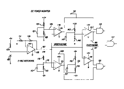
The Powor Monitor Cir¢u$t
The circuitry 63 to monitor the plus and
minus 12v supplies operates from the 5v. supply.
A single red/green bicolor led 64 is connected to
the output of the power monitor circuit 63. The
output indicators are as follows:
LED Indication DescriPtion
Green All voltages present and within
range
Red Elther plu5, minus or both 12
volt supplies are approximately
15% out of spec or dropped out
completely
None +5v supply, all supply voltages
dropped out or no AC
The DC power monitor is a set of four
comparators to check undervoltage and overvoltage
out of range approximately 15% at nominal for the
plus and minus 12 volt supplies. The circuit runs
from plus five volts and uses a plus two volt
precision reference applied to the appropriate
reference input of each comparator. The output is
connected to bicolor LED 64. Precision resistor
~L 3 ~ 3
- 18 -
dividers connected to the other input of each
comparator, scale the test voltage down to the same
range as the reference input.
Fig. 3 is a schematic diagram of the power
monitor for the peripheral repeater. The +S volt
supply is coupled across a series circuit of a
resistor 101 and Zener diode 103. Zener diode 103
is a 1.25 volt Zener diode. The junction between
resistor 101 and zener diode 103 is coupled to the
non-inverting input of an amplifier 105. Amplifier
105 has its output on line 107 coupled through a
resistor 109 to its inverting input. Also coupling
the inverting input to ground is a resistor 111.
In the preferred embodiment, resistor 109 has a
xesistance of 15k and resistor 111 a resistance of
24.3K. This gives a gain for amplifier 105 which
results in a 2 volt output on line 107.
The -12 volt supply is coupled to a
resistor 113 which is in series with a resistor 115
whicX has its other end coupled to the +5 volt
supply. A capacitor 117 is coupled in parallel
across resistor 113. Resistor 113, in the
preferred embodiment, has a value of 15.8K and
resistor 115 a value of 3.01K. If the -12 volt
supply is exactly at -12 volts and the +5 volt
supply at +5 volts, the resulting voltage at the
junction between the two resistors, i.e., on line
~L3~ ~13
-- 19 --
119 will be approximately 2.8 volts. This 2.8
volts is compared with the 2 volts on line 107 in
comparator 121.
The +12 volts supply is coupled to a
resistor 123 in series with a resistor 125 which is
connected to ground. Again, a capacitor 127 is
coupled across resistor 125. The value of resistor
123 in the preferred embodiment is 8.25k and the
value of resistor 125, 2.2k. Capacitors 117 and
127 are each preferably 0.01 microfarad. If the
+12 volt supply is exactly 12 volts, with this
divider, tbe voltage at the junction, i.e., on line
129 will also be above 2 volts. This voltage is
compared in comparator 13~ with the output of line
107.
In the case of comparator 121, the voltage
to the non-inverting input from the voltage
divider, if the full -12 volts is present, will be
above the 2 volts on line 107. This will result in
a high or logic nl~ output from the respective
comparators If the -12 voltage in question
increases, however, above a predetermined amount,
e.g. 15%, at some point the voltage on l~ne 119 as
the case may be, will fall below 2 volts and the
output of comparator 121 will change from a logic
to a logic ~0~. Thus, comparator 121 detects
~n overv~ltage condition for the -12 volt supply.
;
- 20 -
Similarly, if the +12 volt supply drops by,
e.g. 15% the voltage on line 129 will fall below 2
volts and the output of comparator 131 will change
from nl~ to ~0~ indicating~an undervoltage
condition for the +12 volt supply.
To detect undervoltage on the -12 v supply,
an additional voltage divider comprising resistors
133 and 135 is provided. Resistor 133 has its open
end connected to the -12 volts supply and resistor
135, its open end to the +5 volt supply. Once
again, a capacitor 137 is provided. For the +12
supply overvoltage detection, +12 volts is
connected across a voltage divider comprising
reslstors 143 and 14S with the other side of
resistor 145 connected to ground. Again a
capacitor 147 is provided across resistor 145.
Preferably capacitors 137 and 147 have a value of
0.01uf. Resistor 133 has a value of 12.lK,
resistor 135 a value of 3.01X, resistor 143 a value
of 11.8K and resistor 145 a value of 2k. The
ratios in these resistor dividers are chosen such
that if the + and - 12 volt supplies are at their
normal levels, the voltages on lines 139 and 149
respectively will be below the 2 volt reference on
line 107. As a result, the output of the
respective comparators 141 and 151, since the
reference in this case is provided to the non-
inverting input will be positive or a logic ~1~ so
long as the voltage level does not increase above a
predetermined amount. If one of the 12 volt
~3~3~3
supplies goes above a preestablished level, then
the voltage on the inverting input of its
comparator will exceed the voltage on the non-
inverting input and the state of the comparator
will change from a logic ~1~ to a logic ~0~.
Note that for the minus 12 volt comparators
the voltage is biased up with the plus five volt
supply, this is done to keep negative voltages from
being present on the inputs of the comparator.
The outputs of comparators 131 and 151 are
combined in an And gate 153. Similarly, the
outputs of comparators 121 and 141 are coupled to
an And gate 155. The respective outputs of these
And gates 153 and 155 are inputs to an And gate
157. And gate 157 is coupled to the preset input
of a D-type flip-flop 159. The input of this
flip-flop is coupled to ground by a line 161. Its
clear input is coupled to a ~power up~ signal on
line 163 so that the flip-flop is cleared on power
up. Its clocking input is coupled to the output of
an And gate 165 which has as one input a clock
signal obtained from a divide by 16 clock described
in connection with Fig. 4 with a frequency of about
30 KHz and has as its other input, the output of
gate 157.
The logic ~1~ output of flip-flop 159 is
provided as an input to an Nand gate 167 and the
~0~ output to an Nand gate 169. The second inputs
~3~3~ 3
- 22 -
of these Nand gates are a 3 volt signal. The
outputs of Nand gates 167 and 169 are coupled to
pull-up resistors 171 and 173 which are connected
to +5 volts. They are also coupled to the red and
green cathodes of a bi-color T~D 175.
If the voltage levels are as they should
be, there will be no output from gate 157. In that
case, the flip-flop 159 will remain in its reset
state and an output will be provided from its no~
output into gate 169 which will provide a~ on or
ground level to the green cathode turning on the
the green cathode to indicate proper operation.
Should an undervoltage or overvoltage occur, the
output of gate 157 will set flip-flop 159 through
its connection to the preset input. As a result,
an output will be provided on line 177 to the red
cathode indicating that there i8 a problem in the
power supply. The outputs of the four comparators
are normally high and any fault detected will cause
that output to go to low setting flip flop 159.
The power problem can than be diagnosed by checking
the test points 181, 183, 185 and 187 to find out
which comparator is providing a signal indicating a
voltage is not within tolerance. Upon correction
of the defect, the preset signal is removed and the
no~ at the D input, which is connected to ground,
is transferred to the ~1~ output. The ~0~ output
becomes high and the green cathode of LED 125 is
lit.
- 23 -
Thus, as long as a fault condition exists
the clock will be blocked and flip flop 159 will
remain set. However, as soon as the fault
condition goes away the cl~ck will be enabled
loading a zero in and thereby clearing flip flop
157. This has been done so that a transient
condition will not latch up the indicator but
rather that the indicator will indicate a hard
fault condition.
The Function Monitor
As shown in Fig. 2, a tristate LED 61 is
connected to the output of two bit function
register 59. This is used to give visual
indication of what mode or function the PR box is
performing at that time.
LED Indication DescriDtion
. .
Yellow Self-test mode being executed
Red Manufacturing test being
performed
Green Operational mode active
The circuit for driving, function indicator
LED 61, i6 illustrated in FIG. 4. Register 59
indicates which function the PR box is currently
performing, i.e. self-test, operation or
~anufacturing modes. It is a two bit register made
up of a 74LS74 dual D type flip flop using 2 bits
1 3 ~
- 24 -
of a 74LS244 driver for read back. Each flip flop
in the register has both a noninverted and an
inverted output. Thus, the bit 0 flip flop
provides a mode OOL signal-and a mode OOH signal
and the bit 1 flip flop a mode OlL signal and a
mode OlH signal. The read back function has been
added so that correct operation of the register
hardware, exclusive of the LED can be checked
automatically by the self-test software. The
function is indicated by a single bicolor LED 61
operated in a tristate mode to produce three
discrete colors.
A clock signal is provided as an input to a
four-bit binary counter 201 to provide a d~vide by
16 clock output on output line 203. This i8 the
clock which i~ provided as an input to the power
monitor circuit previously described in Fig. 3.
The output on line 203 is provided as an input to a
second four-bit binary counter 205 where the signal
is again divided by 16 to obtain a clock of
approximately 19 KHz. Both counters 201 and 205
are cleared by a power up signal on line 207.
Signals mode 00 lov and mode 01 low from
function register 59 are provided as inputs to a
Nand gate 209. Mode OO corresponds to bit 1 and
mode 01 to bit 2 of two bit register 59.
Similarly, signals mode 01 low and mode 00 high are
provided into a Nand gate 211. Mode 01 high is
provided as an input to a Nand gate 213 which has
?~
- 25 -
as its second input the output of the binary
counter 205. The output of this gate is the clock
input to a D-type flip-flop 215. The nl~ output of
flip-flop 215 on line 217 is coupled as one input
to Nand gate 219. The ~0~ output on line 220 is
coupled as one input to Nand gate 221. These gate
comprise a 75452 dual peripheral driver. The
second input to Nand gates 219 and 221 is a three
volt signal. The output of Nand gate 219 on line
223 is coupled to the red cathode of a bicolor LED
225. Similarly, the output on line 227 is coupled
to its green cathode. Each of the cathodes is
powered by plus 5 volts through resistors 229 and
231 respectively. These are open collector devices
and thus the power for the LED is provided through
the two resistors 229 and 231 tailored to operate
the two LED sections at the same optical
luminescence. Note that the heavier peripheral
driver is required since, re~ardless of which LED
is enabled, current flows through both resistors at
all times.
In operation, if both modes 00 and mode 01
are low, the output of gate 209 will be a logic
and the flip-flop 215 will be preset thereby
providing an output on line 217 which is coupled
through Nand gate 219 to energize the red cathode
of diode 225. If mode 01 is low and mode 00 is
high an output from gate 211 will cause flip-flop
215 to be cleared and an output on line 221 will
result causing the green cathode to be energized.
~3~ ~3 i 3
- 26 -
If mode 01 is high then the clocking signal will be
provided at the output of gate 213. Because mode
01 is high, neither Nand gate 209 or 211 will
provide an output to cause the flip-flop 215 to be
preset or cleared. In a D-type flip-flop, the
clock signal will cause whatever is at the D input
to be transferred to the ~ln output. The D-input
is tied to the ~0~ output on line 221. Thus, if,
for example, line 221 is ~0~ then the ~On will be
transferred to the ~1~ output on line 217 at which
point line 221 will come to a logic ~1~ level. On
the next clock cycle this logic ~1~ will be
transferred to the ~1~ output on line 217. As a
result, the red and green cathodes will be
alternately energized and, because of the clock
rate, it will appear to the observer to be the
color yellow.
PR ~ox Operation ov-r~i-w
The PR box ROM 53 contains self-test and
operational firmware. This firmware is contained
in 4X bytes of ROM, though there is 8K bytes
reserved for it. A listinq of the firmware is set
out in Appendix A. A flow diagram for the firmware
is set out in Figs. 5A-C.
On power-up indicated by block 301, the on
board diagnostics will have control of the PR box
as indicated in block 303. The diagnostics will
perform tests on the PR box logic and do an
external loopback and test if pin 7 on the 8031
port 1 is grounded (signifying manufacturing mode).
In manufacturing mode the diagnostics will loop
forever via loop 305 and not go into operational
mode. This is done via detection of the loopback
connector (pin 7) on power up. If an error is
encountered during manufacturing mode, the
diagnostics will loop forever on the test that
encountered the error.
Registers 55 and 59 with LEDs 57 and 61
(see Fig. 2) attached can be viewed rom the
outside of the system box. Diagnostic register 55
as noted above is 8 bits wide with Red LEDs. These
LEDs report errors for the PR box and/or the
system. As also described, the function rQgister
59 is two bits wide with a single red/yellow/green
LED. When in manufacturing mode, the function LED
is red as indicated in block 303. On power-up,
during other than manufacturing mode, the function
LED will be yellow. In operational mode it will be
green.
The various tests performed on power up are
indicated by blocks 307-314. If in manufacturing
mode, as checked in block 315 of Fig. 5B, the test
of blocks 316 and 317 are also performed before
entering block 318 to loop 305.
~ 3 ~
- 28 -
If, on power up, the PR box has an error
that will make the PR system unusable, i.e.
interrupt, 8031 errors, the function LED will stay
yellow, an attempt to put the error code in the
diagnostic register will be made, and the PR box
will not go into operational mode.
If there are no errors or errors that will
not make the system unuseable, and the system is
not in manufacturing mode, path 320 will be
followed to block 401 of Fig. 5C and the function
LED will turn green and wait for the host to
ACK/NAK, the diagnostic report to establish the
link between the host and the PR box. If the link
is never established, the error code for N0 host is
placed into the diagnostic LEDs, and the PR box
will go into operational mode. If the
communications link is later established, the error
code will be cleared.
If there are soft errors (diagnostic
register or function register) the PR box will go
into operational mode of Fig. 5C and carryout the
background process. However, any LED indication
may be incorrect. Except for a dead system, i.e.
8031 failures, the PR box will attempt to go
operational mode, displaying , if possible, the
point at which it failed the self-test, (test
number).
- 29 -
After the power-up diagnostics have been
completed, control is passed to the operational
firmware. In this mode, the firmware will keep the
link between the host and-the PR box active, and
mux/demux commands/data between the peripherals and
the host. This operation is described in detail
below.
The diagnostics/operating system of this
system are ROM based and run out of the 8031
microprocessor. The PR box firmware is compatible
with the existing peripherals, and adheres to a
communications protocol developed for the host PR
box link discussed below.
The diagnostics are the first part of the
firmware to run on power-up of the PR box. The
diagnostics leave the system in a known Qtate
before passing control to the operating firmware.
Upon comp}etion of testing the PR box, the system
RAM 51 is initialized, queues are cleared, the
UARTs in in OCTALART 67 are set to the default
speeds and data formats, the diagnostic and mode
registers 55 and 57 are set with the appropriate
values, and a system status area is set up that
contains the status of the PR box.
Once the diagnostics are complete, the
diagnostic report is sent to the host, and the PR
box goes into operational mode. If there are no
other messages to send, the PR box will wait 10
- 30 -
seconds for an ACK/NAK before placing an error code
for ~No communications link~ into the diagnostic
register 55. An ACK/NAK timer is provided for all
other packets and times out at 20 mSec. Once
operational, the UARTS are enabled to allow
communications between the peripherals and the
host. A keep-alive timer is also enabled in order
to keep the host link active.
Operational Mode
In this mode, the PR box 21 is the central
communications device sitting between the
peripherals and the host 19. (Refer to Figure 1
block diagram). Before detailing this mode, some
basic terminology and memory allocation utllized on
the PR box must be discu~sed.
A page of memory is 256 bytes in length.
The low order addres~ of the beginning page of
memory is zero, the upper byte is from O to 255.
In this description, the term nport~ is used
interchangeably with ~channel~ and refers to the
peripheral port.
The 8031 has 128 bytes of on-chip RAN. Of
the 128 bytes, 36 are utilized for front, rear,
receive and transmit queue pointers. There is a
front and rear queue pointer for each receive and
transmit queue. Receive and transmit queues are
allocated for each SLU port and the command queue
. .
- 31 -
to the PR box. There are eight ports and one
command channel, thus, there are 18 queues and 36
pointers. Listed below are the names given to the
respective queue pointers;
REAR_RX_QUE_PTR A table
containing the
rear receive
queue pointers
for ports 0-7, &
the cmd que 8
FRONT P.X_QUE_PTR A table
co~taining the
front receive
queue pointers
for ports 0-7, &
the cmd que 8
REAR TX_QUE_PTR A table
containing the
rear transmit
gueue pointers
. ~ ~
for ports 0-7, &
the cmd que 8
~ 3 ~
- 32 -
FRONT_TX_QUE_PTR A table
containing front
transmit queue
- pointers for
ports 0-7, & the
cmd que 8
The receive and transmit queues are
maintained in off-chip RAM. Each queue entry is an
address of the buffer received, or the buffer ready
to be transmitted. Each entry is a word in length,
a word being 16 bits. The first byte is the low
order address, and the second byte is the high
order address. No buffers are moved, only buffer
addresses. Listed below are the names assigned to
critical memory locations.
RX_i_QUE Where i=0 to 7, and
the CMD que-1 page
(256 bytes-128 msg
ptrs)
TX_i_QUE WHERE i=O to 7, and
the CMD que-l page
(256 bytes-128 msg
ptrs)
CHi_BUFFER Where i=O to 7.
Buffer space for each
port. Ports 0 to 7
are the following
sizes 3/4K, 2R, 2R,
l.5X, 3/4K, 3/4K,
3/4K, 2.75K
respectively.
,
'~
- 33 -
RX_BUFFERS 16 bytes (8
addresses, one for
each SLU, there is no
buffer associated
with the command
queue) - Contains the
next free byte in
each ports buffer.
TX_BUFFERS 16 bytes (8
addresses, one for
each SLU, there is no
buffer associated
with the command
queue) - Contains the
next byte to transmit
for each port.
(Transmitter
interrupt sets this
up)
TX SIZE TBL Number of bytes left
to transmit for each
channel. (8
locations)
RX_T~ME OUT Timer bytes for each
receiver channel.
For inter-character
timing. (8
locations)
` :
PORT_TIME OUT Timers for each
channel. Set to lOmS
when a queue is
overflowed. (Port is
turned off for lOmS)
; (8 locations~
: ~ ~
.
,
~ 3 ~
- 34 -
KA_TIMER Keep alive timer. A
10 second timer which
is reset to 10
whenever a packet is
sent to the host. If
the timer times out,
a keep alive packet
is sent to the host.
ACK_NACK_TIMER Timer set to 2OmS
after the checksum on
a packet is sent to
the host. (The timer
is cleared if it
receives an ACK or a
NACX in this time
period. If an
ACK/NACK is not
received, an error
LED is set on the PR
Box.)
The method by which all pointers, queues,
bu~fers, and tables are acceq~ed i8 by getting the
base address (or base page), and adding in the
current channel number (or a multiple of the
channel number). For example, to access the
channel 3 receive queue, the base page of the
receive queues is taken. The upper addre~s e.g.
BASE_Rx PAGE, which i8 the base for all receive
queues is taken and the channel number is added to
it (3 in this case) Once this is done, the value
pointed to by FRONT RX_QUE_PTR p}us the offset of 3
is used as the lower address for the front pointer
of channel 3. The channel number is obtained
easily by reading it from a register in the
OCTALART which, while in an OCTALART interrupt,
.
- 35 -
stores the number of the channel causing an
interrupt. Thus, for exmaple, if data comes in
from channel 3, it causes an OCTALART interrupt.
The channel (3) is stored in an OC~ALART register.
The PR box reads this register and add its value
(3) to the base values and this way guickly and
easily obtains the necessary addresses for the
pointers etc. for channel 3. Thus, a}l the queues,
buffers, etc. can be treated generically by COD on
subroutines, and interrupt routines, with the
exception of Channel 7, which is treated slightly
differently because it is the channel to which the
host is connected.
All queues and buffers are circular. The
queues are circular by virtue of the fact that they
are only one page in length. The upper page
address is loaded directly into the P2 register of
the 8031. The front rear receiver/transmit queue
pointers are loaded directly into register RO or R1
of the 8031 which can be used for external
accesses. Since the pointers are 1 byte, (RO/Rl)
when they are incremented (by 2) from FE hex they
will automatically be set to 0. (FE hex + 2 = lOO
hex, but slnce it i8 a byte value the 1 is tossed
away.) No data checking is necessary because P2
and RO/Rl are separate registers and the one does
not carry to the upper address byte (P2).
: :
'
:~ `
$ ~ 3
- 36 -
Once in operational mode, the PR box will
initialize all the channels to default baud rates
for the peripherals it expects to be on a specific
channel. The default baud-rates are set out in the
table of Fig. 7. Upon this expectation, the PR
box will also allocate buffer sizes to achie~e
maximum processing of data received from and
transmitted to the respective peripherals. The
buffer size is chosen to provide for storage of a
maximum of 256 packets without overwriting buffer
space. This comprises 128 packets in a queue ready
to transmit to the host and another 128 packets in
a peripheral receive queue waiting to be moved to
the host transmit queue. For example, channel 0
buffer is initialized to 768 bytes, (3/4 K), to
accommodate a keyboard which is a single character
device. Each packet stored in the buffer received
from the keyboard will be comprised of three bytes:
channel number, size byte, and the data byte. To
store 256 packets, the buffer allocated is
256 x 3 = 768 bytes (3/4 K) long. Once
communication is established between the host and
the PR box, the host will then interrogate each
peripheral to ascertain what type of peripheral is
connected and make adjustments to the baud rate if
necessary.
The main routine which the PR box runs is
the background process noted above. Fig. 5C is a
flowchart which describes the background process.
~31~ ~3
- 37 -
First, in block 401, on entering this part of the
firmware the function register output is turned to
green.
Then, as shown by block 403 this process
scans the receive and transmit queues to see if
they are empty. It does this by comparing the
front queue pointer to the rear queue pointer for
each queue. If the front equals the rear, the
queue is empty, if they are not equal, then some
action must be taken. The value 1 used in the
background routine is, of course, the channel
number. In this case, i is added to the base
values to get the necessary addresses for checking
the front and rear pointers.
Figs, 6A-E ~llustrate what occur~ when data
is received in a receive gueue ~rom a peripheral
and also illustrate the use of circular queues and
circular buffers according to the present
invention. Fig. 6A depicts the state the queues
and buffers are in initially before a packet is
received. Illustrated is the queue 410 for channel
2; the channel 2 buffer 415 and a t~ble 417
containing pointers for the next available memory
location for each of the receive channels RxO-Rx7
and transmit channels Tx0-Tx7. As noted
previously, data is not moved from buffer to
buffer, only the addresses are moved from queue to
queue. Thus, for channel 2, buffer 2 receives the
data and it is also from this buffer that data is
I
;
3 ~ 3
- 38 -
transmitted to the host. At the start of the
receive for this packet, queue 410 is empty, i.e.,
the front pointer 411 equals the rear pointer 412.
There may have been many packets received before
the front and rear pointers 410 and 411 are at the
top of the receive queue 410 (Rx_2 Queue). The
pointer 416 for Rx2 in table 417 is pointing to the
next free buffer space in buffer 415 which is 44FD
Hex.
Figure 6B depicts what occurs after the
first receive interrupt on channel 2 occurs.
Addresses are obtained in the manner described
above by adding the channel number (2), the base
addresses. A character is read, which in this
example is ~A~. ~he RX ~uffer pointer 416 address
is moved into the RX 2 Queue 410. The packet is
loaded into Channel 2 ~u~fer 415, along with the
channel number 418, the size of the packet 419,
which is initialized to 1, and the character read,
~A~ as indicated at 420. This act causes the
inter-character timer, to be explained in more
detail below, for channel 2 to start.
The next free buffer space is saved in
table 417 of pointer 416. The next free buffer
space pointer is at 3D00 Hex. The last free buffer
-~ space pointer was at 44FF Hex which was the end
location of the buffer. Instead of just bumping
the free buffer space pointer to 4500 Hex and
thereby going into the next SLUs data space and
'~:
.
~31~ ~ 3
- 39 -
losing data, the free buffer space is wrapped to
the start of Channel_2_Buffer. No overrun will
occur because of the size of the packet and number
of packets allowed as described below. This
demonstrates the use of circular buffers in the PR
box software.
The same sequence of events as described
above and depicted in Fig. 6B are repeated as shown
in Fig. 6C and Fig. 6D. The character (B and C)
are read and stored at the start of the channel 2
buffer 415 and the packet size 419 is incremented
accordingly. Each character is moved to the
address in Channel_2_Buffer 415 that pointer 416
~free buffer space poinSer) of the table 417
indicates. Pointer 416 is incremented and the
inter-character timer is re-started. This sequence
of events continues until the inter-character timer
expires.
Figs. 6A-E have been simplified to show
only one packet in each queue at a time. In
reality, each queue may have multiple entries and
each port may be receiving/transmitting packets
concurrently. Having a transmit queue, a receive
queue, a buffer and associated pointers dedicated
to each channel in the PR box makes this operation
possible.
,
13~
- 40 -
Fig. 6E shows that once the inter-character
timer expires, the rear pointer, 412, is bumped to
the next ~ree location (FE Hex + 2 = 00). This
brings the rear pointer to-the start of the queue
thus again demonstrating the use of circular queues
in PR box software as a result of the previously
explained use of the P2 and RO/Rl registers.
All received and transmitted data from the
PR box is handled by interrupt routines. There are
routines, which occur for example, during the steps
of Figs. 6A-6E, to set up the data packets to be
sent from the peripherals to the host. These
packets are considered complete if the number of
characters received for that peripheral equals the
maximum packet size allowed, which is ~ix bytes, or
if there i8 a timeout of the inter-character timer
for that peripheral. For example, the tablet
report size is 5 bytes so after the fifth byte it
will time out and be a completed packet. Inter-
character timeout occurs if approximately two
character times pass without reception of a byte.
Peripheral timeout is handled by inter-
character timers that are initialized before the
initialization code starts. The value that is
loaded into the timer is related to the baud rate.
There is a timer location for each channel. Table
of Fig. 8 contains a list of the timer values used
for the different baud rates. The timer values are
decremented in a timer O interrupt routine,
:::
3 ~ ~ `
- 41 -
described in detail below in connection with Fig.
9. For example, consider the case where the tablet
sends a report which is 5 bytes long at 48Q0 baud.
At 4800 baud and 11 bits per character, it will
take approximately 2.3 msecs per character for
transmission. Then in the case of this report
being sent, the timer would expire after about S
msec and the buffer would be marked as complete.
As disclosed above in connection with Fig.
6B, when the first character is received on ports 0
- 6 (peripheral ports), the address of the first
free space in that ports' buffer 415 is stored in
the queue 410. The current port number is stored
in that location at 418. The next buffer location
419 is the size, and will be initialized to 1.
Finally, the character which was read in e.g. A,
i5 stored in the bu~er. Subsequent bytes are be
stored in the buffer 415, and the size byte 419 is
incremented.
Thus, after each byte is read, a timer for
that port is initialized to approximately twice the
transmit time for a s ngle character. This inter-
character timer value is adjusted if the host
changes the baud rate on any channel. The packet
is closed, and the ith rear pointer 412 of Fig.
6A-E is bumped by 2 when the timer counts to zero
(times out), or the size equals 6, where i is the
channel number, as shown in Fig. 6E.
:
,~
- 42 -
After the background process sees a non-
empty Rx queue, e.g. as in Fig. 6E the buffer
address at the front 411 of the receive queue is
moved to the rear 422 of the Tx_7_Que ~host) 420.
The front receiver pointer 411 of the Rx queue is
bumped to the next location (which may or may not
have any more data buffers to send), and the rear
422 of the Tx_7_Que is bumped to the next free
location. This is shown in Fig. 6F.
In general, the transmitter is turned on
for port 7, if it is not already on, if an ACK/NACK
or a Keep Alive needs to be sent, or the queue is
not empty. If the command queue is not empty, then
the command parser is executed. Transmitter
interrupts turn them~elve~ off when the last
character is sent. The background routine,
transmit, receive, and ti~e interrupts al} run
asynchronously to each other.
Thus, if the receive queue is no*
empty and the queue i8 for port 0 - 6 or the
command queue, then the gueue entry at the front of
that queue is pushed onto the rear 422 of the
transmit queue 420 for port 7. The front 411 of
the receive queue at which the entry was just taken
off is incremented by two as explained above in
connection with Fig. 6F. What has just been
described is h w information is received from a
.. . . .
; ~ .
3~
peripheral into a buffer and the buffer locations
stored in a receive (Rx) queue and then transferred
to the Tx_7_Que to be transmitted to the host.
Packets from the host for the peripherals
(0-6) or the PR box (the command channel) are
handled in similar fashion, first with the
locations stored in the RX_7_Que and then being
transferred to a respective Tx_Que.
If the receive queue for port 7, Rx_7_Que
(the host) is not empty, then the first byte of the
buffer (at the queue entry) contains the port where
the entry should be directed. That port value is
used to select the appropriate transmit queue, and
the buffer address+l is the value which i~ pushed
onto that transmit queue. If the destination is
~or port 7 (i.e., a command to the PR Box), then
this is pushed onto the command queue.
The first character received on port 7 must
be an ACK, NACK, or an SOH. If it i8 an SOH, the
PR Box will expect to receive a packet. All
following characters are stored in the channel 7
buffer. After the last data character is read, the
received checksum is compared with the calculated
checksum. If they are equal, an AC~ is sent to the
host, and the rear pointer for channel 7 is bumped
by 2. If the checksum does not match, or the
inter-character timer expires (10 msec for the
'~ ,
:
1 3 ~
- 44 -
host), a NACK is sent to the host, and the rear
pointer for channel 7 is not incremented (The PR
Box ignores the data it stored).
Once an entry is pushed onto a transmit
queue for ports 0-6 and it is not empty, the
transmitter interrupt is turned on for this
channel, if it is not already on.
A transmit interrupt on ports 0 - 6 will
take the address at the ith transmitter queue front
pointer for the buffer to transmit. The first byte
is the size, which is not transmitted, but the
subsequent bytes are transmitted until the size is
zero. When the interrupt is finished transmitting
all the data bytes, the front pointer for the ith
transmitter is bumped by two, and the interrupt for
that port is turned off.
A transmit interrupt on port 7 could be for
a few reasons such as, to send an ACK, NACK, or a
packet to the host. A transmit interrupt on port 7
(Host port) will reinitialize the keep alive timer
to 10 seconds.
If the PR box is to send a packet to the
host, the first time in the interrupt, it will send
an SOH. The second time in the interrupt routine
it will get the packet address pointed to by the
front pointer 421 for the channel 7 transmitter
queue ~420 as shown in Fig. 6G. The first byte at
~ 3 ~
- 45 -
that address will be the channel which the packet
is from. The PR box takes this byte, sends it and
stores the address of the next byte to send in
Tx Buffers table 417 at the location for channel 7.
For example, Fig. 6G illustrates transmitting the
information for channel 2 which was obtained as
shown in Figs. 6A-E. The next time in, it will
send the size of the packet, and use the size to
send the subsequent data bytes, until the size is
zero. As each byte is sent, the Tx buffer (7) is
incremented to point to the next byte. As each
byte is sent, it is also calculated into the
checksum, and the checksum is then sent when the
size is zero. After the checksum is sent, a timer
is initialized to 20mSec in order to wait for an
ACK or a NACK, and the interrupt is turned off. If
an AC~ i8 received, the ~ront pointer ~or channel 7
will be bumped by two as shown in Fig. 6H. I~ the
timer expires, thîs pointer will be bumped by two,
and tbe LEDs will have the error code to indicate
the host did not respond. Another packet cannot be
sent to the host until an ACK/NACR is received, or
the timer expires.
As noted above, the host sends data to a
physical channel address. The host keeps a table
indicating which device is plugged into a
particular channel. The host can tell which device
is on a particular channel by requesting the device
to send a self-test report. This is done ~or
devices having common connectors that can be
- 46 -
interchanged (i.e., the mouse and tablet, dial box
and digit box, etc.). The PR box tries to
determine if a device is connected to a channel by
looking for the device present bit. The mouse,
tablet, ~uttons box, dial box, and spare keyboard
channels have device present bits. By using these,
the PR box can tell that there is a device out
there, but not what device it is.
When the PR box sends the self-test report,
one byte is the current configuration of the system
(only those devices that have a device present
bit). mere is no attempt made to try to identify
i~ there is a device on the spare channel, host
channel, or the keyboard channel.
A receive interrupt will occur on channels
1 - 4 and 6 if a device 18 plugged/unplugged. If
this occurs, a message is sent to the host. The
ho~t then interrogate~ tbat port to see which
peripheral, if any, is present and records that
information in a table. It then sets baud rates by
sending a command to the peripheral and then a
co~mand to the PR box to ~et the UART baud rate for
the port in question. Baud rates may be reset at
other times by the host to, for example, 910w down
transmission of a data where excessive transmission
errors are encountered.
. ~ `a ~ $
~ 47 --
The Timer 0 interrupt contains the counters
for the inter-character timers, counters for a port
which was previously turned off, and the ACK/NACK
counter. Fig. 9 is a flow diagram illustrating the
Timer 0.
As indicated by Fig. 9, the timer interrupt
occurs approximately every 1.38 msec. Upon the
occurrence of an interrupt, as indicated by block
501, registers are saved and the register banks
changed. The time to the next interrupt is then
loaded as 1.38 msec. as indicated by block 503.
The next step is to get the base address of the
receiver timeout table of intercharacter timers.
This table contains the same information which is
containod in F~gs. 7 and 8 horoof, i.e. for each
channel it givo~ the value for the intercharacter
tim~ng. Tho next block indic~tes that the proces~
starts with i equal to 0. In other words, as block
507 indicates, it ~tarts with channel 0. A
decision block 509 is entered in which~ the first
time through, a check is made to see if the timeout
for receiver i is equal to 0. If it is not equal
to 0, block 511 i~ entered and the timeout i8
decremented by 1. A check is mado again in
decision block 513 to see if timeout has reached 0.
If the an~wer is yes then it is the end of the
message as indicated by block 515 and, as indicated
above, the rear of queue i is bumped. In decision
block 509 if timeout i~ equal to 0 this mean~ there
~ is nothing to be done for this channel. If the
:~:
- 48 -
answer in decision block 513 i8 no, this means that
timeout has not occurred. In either case, block
517 is entered and i is incremented to the next
channel. Following this a decision block 519 is
entered to see if i is egual to 7. If not, the
program loops back by a loop 520 to decision block
509 to check timeout for the next channel. When
channel 7 is reached, as indicated by a yes answer
from block 519, decision block 521 is entered.
Here a check is made to find out if the PR box is
receiving on the host channel. If it is, according
to block 521 timeout is decremented by 1. Then in
block 523 a check is made to see if timeout is
e~ual to 0. If it is, there is a timeout on the
host channel and a number of steps are taken as
indicated in block 525. If timeout has not
occurred, the program proceeds directly to block
527. A~ indlcated therein, a che¢k i8 then made
for a timeout on a port which was turned off. This
is done using the same series of steps just
described.
~ fter passing through block 527, a deci~ion
block i~ entered to see whether or not the PR box
i~ waiting for an ACX or NACX. If the answer in
decision block 529 is no, block 531 is entered
immediately which indicates that the registers are
restored and a return from the interrupt to the
main program. If the PR box is waiting then block
533 is entered and the ACR/NACK timer is
decremented. Next, a check is made in block 535 to
~ ~ 3~3
see if the timer is at 0. If it is not, block 531
is entered. Otherwise, if it is 0, the wait for
ACK/NACK and the transmitter 7 flag is cleared and
the front pointer for the ~ransmitter 7 queue is
bumped as indicated by block 537. Next, block 539
is entered and if it is not system start up the
host gone error is lighted in the LEDs 52 of Fig.
2. After this, block 531 is again entered. As
shown in Fig. 9C, when end message 515 is
encountered, as shown by block 541, the rear
pointer for the receiver associated with the ith
channel for which the message had ended is
incremented by 2. Next, as indicated by block 543,
the receive in progress flag is cleared followed by
clearing of the receive timeout as indicated by
block 545. Next, a check i8 mado in deci~ion block
547 to ~ee if i i~ eqyal to the host channel. If
it i8, the actlon~ t~ken in block 5~9 are carried
out. When this done, or if the answer in block 547
was no, then the progr~m return~ to block 517 of
Fig. 9A. (END_MSG is used elsewhere in the
firmware also.)
A timer i~ only decremented if it i8 non-
zero. If it is non-zero, and transitions to zero,
some action is taken. If an inter-character timer
expires, then the rear pointer 412 for the ith
receiver is bumped by two. If a timer for a port
which was previously off expires, then that port is
turned on. A port is turned off when it gets too
much data, and overflows its queue. The port is
131~ '~13
- 50 -
then turned off for lOmSec. If the ACK/NACK timer
expires, then the front pointer 421 for channel 7
transmitter is bumped by two, and the error for the
host not responding is placed in the LEDs 57.
The Timer 1 interrupt contains the counter
for the ~keep alive~ timer. It is decremented by 1
on each entry. If it transitions to zero, a flag
is set so the background process of Fig. 5C will
send a ~keep alive~ message to the host.
The interrupt routines to receive packets
from the host, thus, set them up in memory for the
bac~ground process of Fig. 5C to decipher. This
backgrou~d process also sets up the process for the
interrupt routine~ to ~end data packet~ to the ho~t
and the peripheral~.
Pac~-t D-flnltion
As noted above, bytes received by the PR
box from a peripheral are grouped into a packet to
be sent to the ho~t. The packet definition is as
follow6:
SON 1 byte: Decimal 1
Header 1 byte: See Fig. 10
t ~1~3~3
- 51 -
Byte Count 1 byte: Number of message/
Message/Data
Text data bytes
Nessage/Report/Data
bytes, length
dependent on peri-
. pheral device
Checksum 1 byte: Checksum for total
transmisison
Response to the above
packet:
ACK/NAK 1 byte: Decimal 6/21
The header byte field i8 illustrated in
Fig. 10.
The three bit device code utilizQs all
available bit~. There are device codes for the
keybo~rd, mouse, tabl~t, dial box, button box, ~R
box system and two spare ports. The host channel
is considered to be part of the PR box sytem, i.e.
the host channel uses a DEV ID of 111.
Code Device
` ~ 000 Keyboard tDEC LK201)
001 Mouse
010 TabIet
011 Dial Box
100 Button Box
101 Spare Channel
110 Spare keyboard
:::
,
:
,~
1 3 ~
- 52 -
111 PR Box including Host Channel
The reception error bit of Fig. 10 is used
to indicate a problem wit~ the associated device
identified by the device code. This bit will be
set when the PR box sees a parity, framing, or
hardware overrun error on the UART associated with
the device.
Reception Error Bit = logical 1 to
indicate an error has occured.
The Reply bit i~ used to indicate the host
that the PR box is responding to a request made by
the host and that the report or data following i8
not being originated by tha PR box or peripheral
device. Thi~ bit is u~ed ~or a response to the
command~ T and R di~cussed bQlow under SQ1~ Test
Command and Status Report Command, respectively.
Reply Bit = logical 1 to indicate this is a
response to a previous request from the host. Used
only for PR box command~.
The Reep Alive bit is used to send null
transmissions to the host within a specified time
(e.g. 10 seconds) if there has been no transaction
in that time period. The host watchdog timer is
set to 10 seconds. This functionality tells the
:
:
~ 3 1 ~
- 53 -
host that the PR box i8 still connected but has not
data to transmit. The host resets its watchdog
timer and starts the cycle again.
Keep Alive - logical 1 to indicate
keep alive function only.
The ~evice Change bit is set to indicate
that a device with a device present bit has been
connected/disconnected to/from the PR box. When
this bit is set, the packet contains one message
byte. This is the configuration byte. The
configuration byte will have one bit set for every
device that has a device present pin that is
plugged into the system.
Device Change Bit - logical 1 to indicate a
device has changed ~t~ts.
The System Error bit is used to send error
reports to the host. When this bit is set, there
is one data byte in the packet. That data byte is
the error code. The error codes that currently
exist are:
1. OlH - Bad command ~ent from ho~t.
2. 02H Device Queue has had an overflow.
Two methods of error detection are
utilized:
1. Checksum for the transmission (add
with carry)
-
1 3 ~ 3
- 54 -
2. Odd parity for each byte.
If the Keep Alive bit is set, the Reply bit
and Error bit are ignored ~y the host. The DEV ID
with Keep Alive must be the PR box device.
Th- Transmission Protoool
The transmission protocol is as follows:
The originating device sends its data and
waits for an ACK (all OK) or a NAK (something
doesn't track, retransmit). Status information is
a little bit different, in that the originating
device, host will be expecting something other than
the ASCII ACK/NAX character back. This i~ where
the Reply bit i~ used.
I~ a NAR i8 recei~ed by elther the PR box
or the host, the source device will retransmit the
previous transmission. The device which sent the
NAK will flush the previoug transmission and
respond to the re-transmission as a new reque~t.
lllu~trative diagra~ are shown in Fig.
llA-C which respectively show host origlnated data:
PR box originated data and a report request by the
host.
When a self-test command is transmitted
directly to a peripheral, i.e. as regular data, the
response coming back will be handled the same way,
.
,
:~''''''' .
~', '.
- 55 -
i.e. as data, and the Reply bit will not be set and
the DEV ID will be that of the peripheral device.
The PR box has no special commands to individually
test individual peripherals.
When a device overrun error occurs, data
may be lost. When the PR box gets an overrun
error, and continues to receive data from that
device before it can empty out it's queue, the
receive for that device is turned off for 10 mSec.
After 10 mSec., the receive is turned on
again, and the data that comes in is placed in the
queue to send to the host. During the 10 mSec.
that receive is off, data i8 lost.
Data fro~ a peripheral i8 limited by the PR
box to a maximu~ of s$x byte~ p r packet. If a
peripheral sends out more than six consecutive data
bytes without any null time period betw en the
bytes, the PR box will make sQparate packets with a
maximum of six data bytes. The packets from the
host to the PR box do not have a data limit check.
However, the host should limit the data size in a
packet to nine data bytQs for ~afety. Th- PR box
can safely store up to 256 packets of nine data
bytes, and warn the host on a queue overflow
condition. If the host ~ends larger packets, it
should send them less frequently, i.e. 128 packets
of 18 data bytes, etc., with a bigger time gap
between packets.
;~
1 3 1 ~ 3
- 56 -
As explained above, packeting of data from
devices is handled by timers. When the PR box
~sees~ a ~null~ time period equal to two times the
character length of a peripheral, the packet is
closed off and placed in the queue to send to the
host. (See the example above.) There is also a
default for a transmission from the host of 10
mSec. null time in between two bytes of a packet.
If this timer expires a NAX will be sent to the
host. If the default speed of the host is changed,
the timer will revert to a time period of two times
the character length.
As previously described, there are also
timers for the Keep Alive (about 10 SECS and
ACX/NAX (about 20 mSec)
Co~can~ to th- PR Box
Self-Te~t Command
T - Test PR Syfitem and send the self-test
report (including the configuration).
Note: Test T will temporarily
disconnect the PR Box from the
host for less than 10 seconds.
,
St~tus R-port Co ~nd
R - Report status of PR System, including
Peripherals configuraiton.
: ;
Chan~e Baud Rat- Co~m~nd (two forms)
O Cnx - where ~n~ is the channel number
(0 - keyboard...7-PR-Host link), and ~'x~ is the
baud rate.
0 Cnxyz - where "n" is the spare channel
(5), "x" is the baud rate, "y~ is the parity (ASCII
0 (Hex 4F) - for odd, ASCII E (Hex 45) - for even,
or ASCII N (Hex 4E) - for none), and ~'z~ is the
bits/char (Hex 5, 6, 7, or 8)/.
Note: The Parity and Bits/char can only
be changed on the spare port,
however, the baud rate on the
spare channel can be changed
without changing the parity and
bit~/char. The other ports can
only have the baud rate changed.
The following is the table of baud rates
(x):
Baud Rate Hex Code
00
01
110 02
134.5 03
150 04
300 05
600 06
1200 07
1800 08
- 58 -
2000 09
2400 OA
3600 OB
4800 OC
7200 OD
9600 OE
19200 OF
Light LBD Comm~n~
Lx - where ~x~ is the bit pattern that will
be displayed in the Diagnostic register LEDs (bit O
is least significant bit).
Note: Only bits 0-6 can be changed by
the u~er. Bit 7 is changed by
the PR Box only. Thi~ bit should
only be used ~or error display.
Though bit 6 can be ch~nged by
the user, caution should be
exerci~ed since this bit is
intended to indicate a system
level error.
'
LFD Display-
Fig. 12 illustrates what the LED registers
will looks like during the various stages that the
-~ PR Box goes through on power up. Six scenarios are
presented.
,
,' ' '
1 3
- 59 -
Diagnost~c ~-port Format
The diagnostic report will look as follows:
1 17 4 X X Y Z Checksum
Where 1 is SOH, 17 Hex is the device ID for the PR
Box with the reply bit set, 4 is the number of data
bytes, the X's are error codes or zero (for no
errors), the Y is the configuration byte, and t~e z
is the Firmware Revision.
Dlagnost~c ~rror Cod-~
Definitions for the PR Box error codes
written to the LEDs with the ~unction ~ED RED.
O 081H-Error encountered in the 8031
0 083H-Error in the diagnostic register
0 083H-Error in the function register
0 084H-Error in the external RAN
0 085H-Error in the checksum of the RON
0 086H-Received an unsolicited interrupt
0 088H-088FH-Error generating or receiving
an interrupt
:~ 0 090H-097H-Error in the DC349 registers
0 098H-09FH-Error in the local loopback
of the DC349
o OAOH-OA7H-Error in the external loopback
for the DC349
o OA8H-OAFH-Error in the DSR or DCD pins
',~
~ 3 ~ 3
- 60 -
of the DC 349 (USed for devie present)
If the communications link between the host
and the PR Box is bad, the-PR Box will report a
code of:
0 04OH-Reported in operational mode if the
host did not ACK/NAK a packet in the
appropriate amount of time. (Not
including Bit 7)
-
.