Note: Descriptions are shown in the official language in which they were submitted.
13~15~
F-1417 C-3896
INTERNAL COMBUSTION ENGINE IGNITION SYSTEM
This invention relates to an electronic
ignition system for an internal combustion engine and
more particularly to an electronic ignition system that
is capable of controlling both the spark timing and
primary current dwell time for a distributorless
ignition system.
In an electronic ignition system a
semiconductor switch is connected in series with the
primary winding of an ignition coil. ~hen the
semiconductor switch is conductive the primary winding
is energized and when the semiconductor switch is
biased nonconductive an ignition spark is developed in
the secondary winding of the coil. The time at which
the primary winding is energized is sometimes termed
the start of dwell SOD and the time at which the
primary winding coil is cutoff is sometimes termed as
end of dwell EOD. The time period between EOD and SOD
is the "off" time of the semiconductor switch and is
sometimes referred to as the anti-dwell period. The
EOD point should occur at the desired spark timing
point to initiate ignition while the SOD point ~hould
be chosen relative to the EOD point that sufficient
energy is developed in the coil to fire a spark plug.
The time period between SOD and EOD iS called the dwell
time and corresponds to the time period that the
primary winding is energized. The system should be
arranged so that this dwell time is sufficient to
~ 3 ~
provide enough energy out of the ignition coil to
reliably fire a spark plug. On the other hand, with a
semiconductor switch controlling primary winding
current the semiconductor switch must be biased into a
current limiting mode in order to limit primary winding
current to a safe value.
It has been recognized in the prior art that
dwell time can be controlled by measuring primary
winding current and then developing a signal that
varies the anti-dwell time so as to maintain a certain
level of current for the primary winding. One such
type of system is disclosed in the United States patent
to LeMasters et al. 3,605,713. In that patent a small
resistor senses primary winding current and places the
output transistor in a current limit mode when the
current limit magnitude is reached. The system further
controls the anti-dwell time and through closed loop
action tends to provide an ultimate primary winding
current magnitude that is substantially equal to the
current limit value. Other arrangements for
controlling dwell time as a function of measured
primary winding current are disclosed in the United
States patents to Mizuno 4,367,722 and to Pagel et al.
, 4,198,936. In Mizuno the ramp time of the primary
winding current is detected and utilized to control
anti-dwell time. In Pagel et al. a counter has pulses
applied thereto during the ramp time of the primary
winding current and the pulses so counted are utilized
subsequently to control the anti-dwell time.
Distributorless ignition systems which
control dwell time are also known. One example of this
is the United States patent to Hachiga et al.
~L 3 ~
4,378,779. In this patent plural ignition coil primary
windings are utilized and a single current measuring
resistor measures the current supplied respectively to
the primary windings. Another patent which relates to
a distributorless ignition system that has dwell
control is the United States patent to Meloeny
4,265,211.
The present invention measures primary
winding current in each of a plurality of ignition
coils in order to control a anti-dwell period.
However, in contrast to the system shown in Hachiga et
al. the system of this invention measures the primary
winding current for a given coil and then controls the
anti-dwell time of this same coil in an arrangement
wherein another coil is energized between energizations
of the given coil. In Hachiga et al. the current is
measured in one coil and is then utilized to control
the anti-dwell period for the next coil to be
energized. Thus, the Hachiga et al. arrangement does
not take into account the fact that the resistance and
inductance of the coils may not be matched. With the
arrangement of this invention data is collected for a
given coil and is then not utilized until the time for
controlling the anti-dwell period of this same coil.
Accordingly it is an object of this invention
to provide a dwell control for a distributorless
ignition system wherein primary winding current data is
collected for a given coil and then is subsequently
used to control the anti-dwell period for the same
coil.
Another object of this invention is to
provide a dwell control system wherein the ramp time of
~3~5~
the primary winding current is measured and wherein one
of a plurality of current limit times are selected as a
function of the ramp time. The current limit time that
is selected is utilized to control an anti-dwell period
and the system is arranged such that the current limit
time selected is of such a value as to cause the dwell
time to be long enough to cause primary winding current
to attain a current limit value.
Still another object of this invention is to
provide an ignition system that has a dwell control
arrangement which is under certain conditions of
operation operates to extend the EOD point from a
calculated EOD point. The conditions of operation
which determine whether or not the EOD is extended are:
A. A determination of whether or not the
primary winding current has reached its
current limit value when the EOD signal
occurs;
B. Determining whether the ramp time of the
primary current has exceeded a certain
time value; and
C. Whether or not the SOD signal has occurred
during a minimum burn time or "off" time
of the semiconductor switch that controls
primary winding current.
By extending the EOD point from the
calculated EOD point the dwell time is increased to
assure sufficient coil energy to fire a plug. The
extending of the EOD point may be caused, for example,
by a sudden change in spark timing or by sudden engine
acceleration.
Another object of this invention is to
provide a dwell control system which operates to
increase a subsequent occurring dwell time when the
system operates to extend EOD from the calculated EOD.
IN THE DRAWINGS
Figure 1 illustrates an internal combustion
engine ignition system made in accordance with this
invention;
Figure 2 illustrate waveforms which are
developed in various parts of the ignition system
illustrated in Figure 1;
Figure 3 is a schematic circuit diagram of a
part of the circuit that has been illustrated as a
block in Figure 1;
Figure 4 illustrates the dwell and advance
control of the ignition system of this invention which
is illustrated as a block in Figure 1;
Fig~re 5 illustrates the contents of a ramp
counter that is used in the ignition system of this
invention when the system is operating in the bypass
mode; and
Figure 6 is similar to Figure 5 but
illustrates the contents of a ramp counter when the
system is operating in an EST mode.
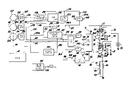
Referring now to the drawings, and more
particularly to Figure 1, the reference numeral 10
designates a four cycle internal combustion engine. In
the description of this invention the engine 10 will be
considered to be a 4 cylinder engine having a firing
order 1-3-4-2. The reference numerals 12 and 14
designate spark plugs which are respectively associated
with cylinders 1 and 4 of the engine 10. The reference
numerals 16 and 18 designate spark plugs that are
1 3 ~
respectively associated with cylinders 2 and 3 of the
engine 10.
The ignition system of this invention is a
so-called distributorless ignition system in that it
does not utilize the conventional rotor and distributor
cap contacts for sequentially distributing spark firing
energy to the spark plugs of the engine. To this end,
the spark plugs 12 and 14 are connected to the
secondary winding 20 of an ignition coil C1 and the
spark plugs 16 and 18 are connected to the secondary
winding 24 of an ignition coil C2. The ignition coil
Cl has a primary winding 28 and the ignition coil C2
has a primary winding 30. One side of the primary
windings 28 and 30 are connected to a conductor 32
which in turn is connected to the positive side of
direct voltage source 34, which is illustrated as a
battery. The negative side of source 34 is grounded
and the source 34 may be the storage battery on a motor
vehicle which is connected to a battery charging
generator (not illustrated). The generator also
supplies the electrical loads on the motor vehicle
including the ignition system in a manner well known to
those skilled in the art.
The ignition system comprises two
semiconductor switches that take the form of Darlington
connected transistors 36 and 38. Darlington transistor
36 is comprised of NPN transistors 36A and 36B and
Darlington transistor 38 is comprised of NPN
transistors 38A and 38B. The transistors 36 and 38 are
respectively connected in series with the primary
windings 28 and 30 and in series with a current sensing
resistor 40 which has a low resistance value, for
~ 3 ~
example of .047 ohms. A resistive voltage divider is
connected across resistor 40 comprised of resistors 41
and 43 that have a junction or node 45. The resistors
41 and 43 have resistance values which may be in a
range of about 19 to 35 ohms. The resistors 41 and 43
are laser trimmed to predetermined resistance values
for the purpose to be described hereinafter. When the
Darlington connected transistor 36 is biased conductive
a current path can be traced from conductor 32, through
primary winding 28, through the Darlington connected
transistor 36, through conductor 42 and then through
resistor 40 to ground. When the Darlington connected
transistor 38 is biased conductive a current path can
be traced fro~ conductor 44, through primary winding
30, through the conductive Darlington connected
transistor 3% and then through resistor 40 to ground.
It will be evident that when a Darlington connected
transistor 36 is biased nonconductive a high voltage
will be induced in secondary winding 20 which will
cause spark plugs 12 and 14 to be fired in series. In
a similar fashion when Darlington connected transistor
38 is biased nonconductive a high voltage will be
induced in secondary winding 24 to cause the spark
plugs 16 and 18 to be fired in series.
It will be evident from the foregoing that
two spark plugs, corresponding to two cylinders of the
engine, are fired iQ series each time that a respective
Darlington connected transistor is biased
nonconductive. The system is arranged such that when a
spark plug, associated with a cylinder that is in its
compression stroke, is fired another plug associated
with a cylinder that is in its exhaust stroke is
~L 3 ~
simultaneously fired. Thus, if the piston of the
cylinder associated with spark plug 12 is in its
compression stroke the piston of the cylinder
associated with spark plug 14 will be in its exhaust
stroke and vice versa. The same holds true for the
cylinders that are fired by spark plugs 16 and 18.
In order to properly synchronize the
simultaneous spark plug firing of cylinders 1 and 4 and
cylinders 2 and 3, as a function of piston position,
the ignition system of this invention develops voltages
that are related to engine crankshaft position. To
this end the engine crankshaft 46 is mechanically
connected to a pair of disks 48 and 50 which
respectively have slots 50A and 48A. The disks 48 and
50 cooperate, in a known manner, with pickup coils 52
and 54 to cause a voltage to be induced therein each
time that a slot passes a pickup coil. The pickup
coils are coupled respectively to squaring circuits 56
and 58 which cause pulses of voltage to be applied to
20 lines 60 and 62. The slots 50A and 48A are spaced 180
from each other so that the voltage pulses developed on
conductors 60 and 62 are 180 out of phase.
, The voltage pulses on conductors 60 and 62
are applied to a flip-flop 64, the output terminals of
which are connected respectively to AND gates 66 and
68. The outputs of the AND gates are applied to a
control circuit 70 via inverters IN1 and IN2 and
conductors 72 and 74. The control circuit 70 is
illustrated in detail in Figure 3. The control circuit
30 70 is also connected with conductors 71, 76, 78, 80 and
82, all of which are also illustrated in Figure 3.
~ $ ~
The voltages developed on conductors 60 and
62, the flip-flop 64 and the AND gates 66 and 68
provide a synchronizing arrangement which will permit
the Darlington connected transistor 36 to control the
firing of spark plugs 12 and 14 during a given 180
rotation of crankshaft 46 and which will permit
Darlington connected transistor 38 to control the spark
firing of spar~ plugs 16 and 18 during another 180
rotation of crankshaft 46. What has just been
described may be termed a bank selector since it
selects either the bank of cylinders 1 and 4 or the
bank of cylinders 2 and 3 for spark plug firing in
synchronization with crankshaft position. This bank
selector arrangement can take known forms other than
1S the arrangement that has been described and the
specific manner of bank selection does not form a part
of this invention.
The transistors 36 and 38, when initially
biased conductive, are biased to a fully saturated
condition. This being the case, the current through
the primary winding is limited by the resistance of a
given primary winding and the very small resistance of
the resistor 40. Figure 2C depicts primary winding
-' coil current as a function of elapsed time. When a
Darlington connected transistor 36 or 38 is biased
conductive, the current increases from zero along a
ramp function identified by reference numeral 84 in
Figure 2C. As the current increases from zero along
the ramp curve 84 the voltage developed across the
small resistor 40 and consequently the voltage at
junction 45 will follow the ramp function 84. The
voltage at junction 45 is applied to the control
1 3 ~
circuit 70 via the conductor 80 and when the current
level reaches a value designated by reference numeral
88, in Figure 2C, the transistors 36 or 38 are brought
out of saturation and become biased into a current
limiting mode. In the current limiting mode, the
current remains at the level designated by reference
numeral 88 in Figure 2C. When the current reaches the
current limit value 88 of Figure 2C, the control
circuit 70 outputs a signal on line 82 which is
utilized to control the ignition system in a manner to
be more fully described hereinafter.
When a Darlington transistor 36 or 38 is
biased nonconductive the primary winding is deenergized
and consequently the primary winding current drops to
zero. This is depicted by the portion of the current
curve designated as 89. When primary current is
cutoff, a pair of spark plugs are fired. In Figure 2C
the time period required for coil current to rise to
the current limit value is identified as RT. This time
period will be referred to hereinafter and can be
termed the rise or ramp time of primary winding
current. Figure 2C also depicts the time period that a
transistor 36 or 38 is operating in the current limit
mode. This time period has been identified as CLTE and
it corresponds to the flat portion 91 of the coil
current curve where primary current does not vary with
the passage of time.
The control circuit 70, which is illustrated
in detail in Figure 3, will now be described. This
control circuit has two identical parts or sections
generally designated respectively as 90 and 92 which
respectively control the switching of transistors 36
13~
and 38. A conductor 94, which is common to sections 90
and 92, is connected to the positive side of direct
voltage source 34 by resistor 96 and conductor 71. A
pair of PNP transistors P13 and P14 have their emitters
connected to conductor 71. The bases of these
transistors are connected to a constant current source
(not illustrated) via conductor 98. The collector of
transistor P13 is connected to a node or junction 100
and the collector of transistor P14 is connected to
junction 102. The purpose of transistors P13 and P14
is to provide a constant current source arrangement.
The section 90 has a PNP transistor P17
connected between conductor 94 and a junction or node
104 that is connected to the base of Darlington
transistor 36 via conductor 76. An NPN transistor N27
has its collector connected to junction 104 and its
emitter connected to ground. When transistor Pt7 is
conductive it supplies sufficient base current to
transistor 36 to cause it to become saturated or fully
conductive. When transistor N27 is biased conductive
it shunts the base drive to transistor 36 and causes
the base current to transistor 36 to be reduced to such
a level that transistor 36 is biased out of saturation
and into a current limit mode. Accordingly, the
primary winding current is limited to a constant value
or level 88 shown in Figure 2C. Whenever transistor
P17 is biased fully nonconductive base drive to
transistor 36 is cutoff with the result that transistor
36 is biased fully nonconductive to thereby interrupt
the primary winding circuit and cause a voltage to be
induced in the secondary winding 20 that causes spark
plugs 12 and 14 to be fired in series.
3 ~
The circuit section 90 has PNP transistors
P15 and P16, NPN transistors N23, N24, N25 and N26 and
a plurality of resistors, all connected as shown in
Figure 3. The base of transistor N23 is connected to
control junction 100 by resistor R34 and diode D4.
When the voltage at junction 100, and hence on the base
o~ transistor N23, is at a low level the transistor N23
is biased nonconductive. When transistor N23 is biased
nonconductive it causes transistor P17 to be biased
conductive and conse~uently Darlington transistor 36 is
biased conductive. When the voltage on junction 100
goes to a high level transistor N23 is biased
conductive causing transistor P17 and Darlington
transistor 36 to be biased nonconductive. In summary,
Darlington transistor 36 is biased conductive for a
period of time that corresponds to the period of time
that the voltage at junction 100 is at a low level.
This time period is the so-called dwell time since,
during this time period, primary winding 28 is
energized. The period of time that Darlington
transistor 36 is biased nonconductive corresponds to
the period of time that the voltage on junction 100 is
at a high level.
The control section 90 has an NPN transistor
N22. The collector of this transistor is connected to
line 71 via resistor R32. The emitter of transistor
N22 is connected to the base of transistor N27 and to
junction 106. A resistor R35 is connected between
junction 106 and ground. The base of transistor N22 is
30 connected to conductor 108 via resistor R31. When
transistor N22 is biased conductive it biases
transistor N27 conductive. The conduction of
transistor N27 causes the Darlington transistor 36 to
be pulled out of saturation and biases transistor 36
into the current limiting mode where current is limited
by transistor 36 to the level 88 shown in Figure 2C.
The switching state of transistor N22 is
controlled by a part or section of the control circuit
70 which has been generally designated as 110. This
circuit responds to the voltage at voltage divider
junction 45, shown in Figure 1. The circuit section
110 comprises a PNP transistor P1, NPN transistors
N1-N6, a plurality of resistors, a capacitor C and
diode D1. The circuit 110 develops a reference voltage
at junction 112 which is applied to the base of
transistor N5 through resistor R8. The emitter of
transistor N5 is connected to voltage divider junction
45 (Figure 1) via conductor 80. When the voltage
applied to the emitter of transistor N5 from junction
45 increases to a predetermined value the amount of
current conducted by transistor N5 is decreased. This
corresponds to a level of primary winding current 88
(current limit) shown in Figure 2C. When the
conduction of transistor N5 is reduced or decreased the
amo~nt of current conducted by transistor N6 is
increased and accordingly the voltage on conductor 108
goes to a high level. The increased conduction of
transistor N6 causes transistors N22 and N27 to conduct
and Darlington transistor 36 is biased out of
saturation and into its current limiting mode. The
voltage on conductor 108 is applied to line 82 and this
voltage indicates whether or not a Darlington
transistor 36 or 38 has been biased into the current
limit mode. The voltage on lines 108 and 82 is at a
~ 3 ~
high level for a period of time that corresponds to the
time period that Darlington transistor 36 is operating
in its current limit mode and the point of the low to
high voltage transition of this voltage occurs when the
current limit is reached.
The circuit section 92 controls the switching
state of Darlington transistor 38 and since it is
identical with circuit section 90 it will not be
described in detail and most of the elements have not
been designated by reference indicia. The circuit
section 92 has transistors P12 and N21 which perform
the same function as transistors P17 and N27 of circuit
section 90. Transistor N16 has its base connected to
line 108 via resistor R24 and this transistor performs
the same function as transistor N22. Junctions or
nodes 114 and 116 of circuit 92 correspond to junctions
100 and 104 of circuit section 90. Transistors P8 and
P9 perform the same function as transistors P13 and
P14.
During the manufacture of components of the
ignition system of this invention the resistors 41 and
43 (Figure 1) are laser trimmed to values such that the
,' system will properly respond to bias transistors 36 or
38 into a current limit mode and cause a current limit
signal voltage to be developed at conductors 108 and 82
when a predetermined magnitude of primary winding
current is attained. Assuming, by way of example and
not by way of limitation, that a transistor 36 or 38 is
to be biased into a current limit mode when primary
winding current reaches 9 amps the resistance values of
resistors 41 and 43 are adjusted by trimming these
resistors such that when 9 amps flow through resistor
40 and parallel connected resistors 41 and 43 the
voltage developed at junction 45 will be of a value to
cause transistor N6 (Figure 3) to be biased conductive
to thereby bias transistor 36 or 38 to its current
limit mode and cause a signal voltage to be developed
on conductors 108 and 82. With an assumed current
limit level of 9 amps the current level 88, shown in
Figure 2C, will represent 9 amps of primary winding
current.
Referring back now to Figure 1, a wheel or
disk 12G is illustrated which is driven by the engine
crankshaft 46. This wheel or disk has six slots which
are spaced 60 apart. As the disk 120 rotates, pulses
of voltage are induced in a pickup coil 122 which are
applied to a squaring circuit 124. The output of the
squaring circuit 124 is applied to a line 126 and these
pulses are depicted in Figure 2A. The pulses, as shown
in Figure 2A, are 60 crankshaft degrees apart and some
of the pulse edges of the pulse train shown in Figure
2A occur at a top dead center position of a pair of
pistons. These top dead center positions have been
identified as TDC and they occur at each 180 of
crankshaft rotation. The 60 pulses shown in Figure 2A
are converted to a waveform shown in Figure 2B by a
signal converter circuit 128. The output of the signal
converter circuit 128 is applied to conductor 130 and
is illustrated in Figure 2B. This signal has
repetitively occurring voltage transitions 130A, 130B
and 130C. The voltage transitions 130A and 130C occur
at top dead center positions of a pair of pistons
whereas the voltage transition 130B occurs at a
crankshaft angle that is 60 before top dead center.
13 ~ $
The voltage transitions 130C and 130A are spaced by
180 of crankshaft rotation.
The system of Figure 1 has an electronic
control module 132, hereinafter referred to as an ECM.
The ECM 132 takes the form of a programmed
microprocessor which is capable of providing spark
timing information for controlling the spark timing
advance. The ECM is well known to those skilled in the
art and may be of a type disclosed in the United States
10 patent to Motz, 4,231,091 granted on October 28, 1980.
The ECM has its own clock pulse source and it computes
time periods in a manner known to those skilled in the
art.
The ECM 132 responds to the high to low
voltage transitions 130B illustrated in Figure 2B.
These transitions provide reference pulses for the ECM
and the ECM computes spark advance value relative to
these pulses. The ECM further receives engine speed
information via lines 134 and 136. These lines provide
the ECM with the 60 pulses shown in Figure 2A. In
addition, the ECM receives other information from the
engine 10 via a line 138. This information may
include, for example, engine temperature and engine
manifold pressure and other factors well known to those
skilled in the art.
When the ECM 132 is controlling spark advance
(EST mode of operation) it develops a signal on line
140 which causes a spark firing event to occur, that is
it causes one of the Darlington transistors 36 or 38 to
be biased nonconductive.
The engine speed pulses on line 134 are
applied to an engine speed switch 142. The engine
16
speed switch 142 develops a control signal on line 144
which controls gate 144A. When the gate 144A is closed
both the dwell and the spark timing are now controlled
solely by the waveform illustrated in Figure 2B. With
gate 144A closed the Figure 2B pulses are applied to
AND gates 66 and 68 via line 146, inverter IN3, closed
gate 144A, line 147, junction 149 and lines 151 and
153. Thus, when gate 144A is closed an ignition coil
is energized at the occurrence of the voltage
transition 130B and is deenergized at the occurrence of
voltage transition 130A. The net result of this is
that an ignition coil is energized for 60 of
crankshaft rotation and an ignition spark occurs at top
dead center. This condition will occur when the engine
is being cranked prior to starting.
When gate 144A is open the time of spark
firing will be controlled either from the bypass
advance circuit 143 or by the EST output signal on line
140. When the EST signal is controlling, the system is
in the so-called EST mode and when the output of bypass
advance circuit 143 is controlling the system is
operating in the so-called bypass mode. The system is
arranged such that when the ECM is operating properly
' the EST signal on line 140 is applied to the dwell and
advance control 150. However, in the event of a
failure of the ECM, or certain other malfunctions, a
bypass control signal is developed on line 152 which
controls gates G1 and 144A. The bypass control signal
is also developed when the engine is being cranked.
When gate G1 is closed the EST signal on line 140 is
aplied to the dwell and advance control 150 via line
145. During engine cranking the bypass control signal
~ 3 ~ ~ r~
on line 152 causes gate Gl to be open and gate 144A to
be closed. At this time the bypass signal on line 152
and the speed signal on line 144 are applied to gate
144A to cause this gate to be closed. When the system
is operating in the bypass mode and engine speed is
above 400 rpm gates G1 and 144A are opened. The output
of bypass circuit 143 now controls spark timing and it
is applied to dwell and advance control 150 via line
155.
The bypass control circuit 143 develops an
output binary control signal that represents a
programmed constant time period. The system is
arranged such that the spark advance signal developed
by circuit 143 causes spark advance, in terms of
crankshaft degrees, to be increased with increasing
engine speed. When the bypass advance timing is
utilized the spark timing is controlled solely as a
function of engine speed.
The gating circuit for controlling the
various modes of operation, i.e., bypass mode, EST mode
and cranking mode can take various forms other than the
one that has been described as long as the following
conditions are met.
(1) During the bypass mode with engine speed
below 400 rpm spark timing and dwell
time are controlled exclusively by the
pulses shown in Figure 2B. This will
occur when the engine is being cranked.
(2) During the bypass mode and with engine
speed above 400 rpm spark timing is
controlled by the output of bypass
advance circuit 143.
18
~ 3 ~
(3) During the EST mode spark timing is
controlled by the EST signal on line
145.
The dwell and advance control 150 is
illustrated in Figure 4 and will now be described.
Referring to Figure 4, it is seen that the system has
an anti-dwell ripple counter 154 coupled to a digital
comparator 156. The digital comparator is a so-called
start of dwell comparator and develops a signal on line
158 which will hereinafter be referred to as the SOD
signal. When an SOD signal is developed on line 158 it
will cause a corresponding SOD signal to be developed
on line 160, illustrated in Figures 1 and 4. When the
SOD signal appears, one of the output transistors 36 or
38 is biased conductive to initiate energization of a
primary winding of an ignition coil.
The system of Figure 4 has another digital
comparator 170 which is a so-called advance comparator.
The advance comparator develops an end of dwell signal
EOD1 on li~e 172 which is developed at the desired
spark timing angle and which, under certain modes of
operation, wili immediately cause one of the
transistors 36 or 38 to be biased nonconductive. This
signal on line 172 is applied to an EOD developing
25 control circuit that includes a gate 174. The gate 174
responds to the bypass control signal on line 152, the
speed signal on line 144 and the signal on line 130
which is illustrated in Figure 2B. The gate 174 is
closed whenever the system is operating in the bypass
mode and engine speed is above 400 rpm. Further, the
gate 174 is closed only during the time that the signal
shown in Figure 2B is at a low level, that is for a
19
period of 60 before top dead center~ The output of
gate 174 is connected to gate 175 via a line 177. A
signal EO~3 is developed on line 177 and the output of
gate 175 develops an EOD2 signal on line 176. As will
be explained more fully hereinafter the EOD2 signal
will be developed on line 176 at the same time that the
EOD3 signal appears on line 177 or will be developed on
line 176 at a point delayed from the development of the
signal on line 177.
The system of Figure 4 has a clock 180 for
developing constant frequency clock pulses on line 182.
The clock frequency may be about 31.25 Khz. The clock
pulses on line 182 are applied to a TACH COUNTER 186
which is controlled by the 60 pulses of Figure 2A
applied thereto by conductor 134A. Conductor 134A is
connected to conductor 126 by conductor 134 as
illustrated in Figure 1. The TACH COUNTER counts the
constant frequency pulses on line 182 for each period
of 60 of crankshaft rotation and loads the count so
counted into the 60 TACH LATCH or register 192 at the
end of a 60D period and then counts again for a 60
period. Each time a 60 period occurs the pulses so
counted are loaded into the 60 TACH LATCH register
192. The 60~ latch 192 therefore contains and stores a
pulse count that is a function of the clock frequency
of clock 180 and the time that elapses during 60
degrees of rotation of crankshaft 46. The pulse count
developed by TACH COUNTER 186 is also applied to line
194 and hence to advance comparator 170.
As previously mentioned, the ignition system
of this invention can operate in either the bypass mode
or in the EST mode. In either mode the dwell time is
~ $ ~ 3
controlled. The dwell control arrangements for each
mode are similar but not identical. The advance and
dwell control, when the system is operating in the
bypass mode, will now be described.
When operating in the bypass mode a binary
number that represents the programmed bypass advance
time AT developed by bypass advance circuit 143 is
applied to the full adder 196 by line 155. The output
of the 60 LATCH 192 is also coupled to full adder 196
and the output of adder 196 is connected to advance
comparator 170 by line 197. The digi~al number applied
to line 155 represents the 2's compliment of the
progrmmable advance time which results in a subtraction
of the advance time from the 60D time. The contents of
the TACH COUNTER 186 are compared to the sum outputs of
the full adder 196 by comparator 170. The TACH COUNTER
is reset at 60 before initial timing and starts
incrementing up. When the count of TACH COUNTER 186
becomes equal to the sum outputs of the full adder 196
the end of dwell point is reached and accordingly the
signal EOD1 on line 172 is developed. When the signal
EOD1 is developed it may cause an immediate spark plug
firing or the spark plug firing may, under some
~ conditions of operation, occur at some time period
after the occurrence of EOD1 in a manner that will be
described hereinafter. It will be appreciated that
since the advance time AT is a constant value, spark
advance, in terms of engine crankshaft degrees, will
increase with increasing engine speed.
The dwell control arrangement, when the
system is operating in the bypass mode, will now be
described. The dwell control system includes a ramp
21
~ 3 ~ ~, r3 ~ ~
counter 200 which is connected to a gate 202 via OR
gate 281 and line L1. When gate 202 is closed the
counter 200 is connected to clock 180 by a divide by 3
divider 201 and OR gate 281 so that the ramp counter
200 is clocked at 1/3 of the frequency of clock 180 via
line L1. The gate 202 may be closed for the time
period RT or in other words for a period of time
corresponding to the time that elapses from initiation
of primary winding current until the current reaches
the current limit value. In order to accomplish this a
flip-flop 203 is provided which responds to an SOD
signal on line 158 and to a signal on line L3. The Q
terminal of flip-flop 203 is connected to gate 202 and
its QB terminal is connected as one input of an AND
gate 282. The gate 202 is closed for a period of time
in which a signal is developed on the Q terminal of
flip-flop 203. The line L3 is connected to the output
of an OR gate OR1. One of the inputs to the OR gate
OR1 is the line 81A which has the current limit signal
applied thereto. The other input to O~ gate OR1 is the
line 176 which is the EOD2 signal applied thereto. The
line 81A is the output of flip-flop 81 shown in Figure
1. The output waveform of flip-flop 81 is identified
as 81B and it has a leading edge 81C and a trailing
edge 81D. The leading edge 81C occurs when current
limit is reached and the trailing edge 81D occurs at
the end of dwell. The R terminal of flip-flop 81 is
connected to a NOR gate NG1 the inputs of which are
connected to the outputs of AND gates 66 and 68. The S
terminal of flip-flop 81 is connected to line 82 and as
will be recalled, the voltage on this line increases to
a value sufficient to trigger flip-flop 81 when current
i ~ 3 ~
limit is reached. If the current limit signal CL is
developed on line 81A before the end of dwell signal
EOD2 is developed on line 176 clock pulses will be
counted by ramp counter 200 for the time period RT.
The number of pulses counted by counter 200, under this
condition of operation, therefore corresponds to the
time period RT.
The ramp counter 200 is coupled to a
programmable logic array 204 that serves to develop a
binary signal that corresponds to the magnitude of the
binary signal attained by counter 2000 Programmable
logic arrays are well known to those skilled in the art
and in general comprise an array of logic gates that
are connected to a plurality of input lines and a
plurality of output lines. A binary signal applied to
the input lines will result in the development of a
programmed binary signal on its output lines. One
example of a programmable logic array is disclosed in
the United States patent to Reyling et al., 3,949,370.
20 The PLA 204 responds to the attained binary count in
ramp counter 200 that corresponds to time RT and
develops a binary current limit time signal CLT based
on the magnitude of the time period RT. The PLA 204
develops one of three different current limit time
25 signals CLT1, CLT2 or CLT3, the magnitudes of which
depend upon the ramp time RT. Thus, the PLA 204
operates as a digital function generator which develops
a CLT signal as a function of the magnitude of the ramp
time. The CLT signal that is developed by PLA 204 is
applied to a current limit storage register 205 by line
L2 where it is stored for use in a manner to be
described. As mentioned, the binary output signal of
PLA 204 represents one of three different time periods
CLT1, CLT2 or CLT3. The arrangement is such that as
the ramp time increases the current limit time that is
developed by PLA 204 will increase. By way of example,
and not by way of limitation, the following table sets
forth the three current limit times for various ranges
of ramp time.
RAMP TIMECURRENT LIMIT TIME (CLT)
_
0 to 3.8 ms780 ~s
3.8 ms to 4.5 ms 970 ~s
4.5 ms to 23 ms 1642 ys
The digital binary output signal (CLT) of PLA 204
is periodically loaded into CLT storage register 205
immediately after ramp counter 200 has counted the time RT.
The binary number that is stored in CLT storage register 205
represents a time period that is related to the ramp time RT
of a given coil. As will be more fully explained
hereinafter the binary number loaded into storage register
205, for a given coil, is later utilized to control the
start of dwell for this same coil. Thus, if it is assumed
that the data in register 205 corresponds to the ramp time
of coil C1 the digital number stored in register 205 will be
utilized to control the start of dwell of coil C1. This is
an important feature of the invention since the data
collected for a given coil is utilized to control the time
that the same coil is energized. Since the resistance and
inductance of coils C1 and C2 may not be matched, the system
of this invention accommodates for any such variation since
it collects data in regard to a given coil and then utilizes
this at a later time to control the start of dwell of this
same coil.
24
~ 3 ~ g
In order to further explain the operation of the
system shown in Figure 4 it is pointed out that the system
has a minimum burn counter 260. The minimum burn counter
has clock pulses applied thereto via line 182. The counter
260 also receives the end of dwell signal EOD2 on line 176.
The counter has two outputs, namely line 261 and line L4.
The line L4 is connected to one-shot multivibrator OS2 and
line 261 is connected to AND gate 262. When an EOD2 signal
is applied to counter 260 it starts counting clock pulses.
After the elapse of a time period of about 500 microseconds
the counter develops a signal BC on line L4 which triggers
the one-shot OS2. The one-shot OS2 is therefore triggered
500 microseconds after the occurrence of EOD2. The counter
260 develops a signal on line 261 after the elapse of a
period of time of about 700 microseconds from the occurrence
of EOD2. The counter 260 and associated circuitry will be
described in more detail hereinafter.
The system of Figure 4 has latch circuits LA1 and
LA2. Latch LA2 is connected to the CLT storage register 205
and the load control terminal of this latch is connected to
the output of one-shot multivibrator OS3. Latch LA2 is
connected to latch LA1. Latch LA1 is connected to preloader
circuit 208 and is also connected to the programmable logic
array 204. The load control terminal of latch LA1 is
connected to the output of one-shot multivibrator OS2 by a
line L10. The output of one-shot OS3 is connected to a
one-shot multivibrator OS5 which is connected to a reset
terminal of CLT storage register 205. The programmable
logic array 204 is also connected to the output of a gate
circuit G5. The gate circuit G5 is connected to one-shot
OS2, to the programmed bypass advance signal AT on line 155
and the bypass control signal 152. When the system is in
the bypass mode the gate G5 will gate the AT signal into the
PLA 204 at the time that an output signal is developed by
one-shot OS2. Thus, the gate G5 responds to the bypass
control signal 152 and the output of one-shot OS2. When the
system is in the EST mode the gate G5 is in a condition
(open) that will not allow signal AT to be gated into PLA
204. In the EST mode the signal at latch LA1 is applied to
PLA 204 when the one-shot OS2 develops an output.
With the foregoing in mind let it be assumed that
an end of dwell signal BOD2 has been developed on line 176.
This signal is developed when one of the transistors 36 or
38 is to be biased nonconductive to cause a spark to be
developed. Let it be assumed that primary of coil C1 has
been deenergized to cause plugs 12 and 14 to be fired. The
signal EOD3 triggers one-shot OS1 and signal BC on line L4
triggers one-shot OS2. One-shot OS2 triggers one-shot OS3.
When 0S3 is triggered or actuated it causes a PLA preloader
circuit 208 to load ramp counter 200 via line 210. When
one-shot 0S3 is actuated preloader circuit 208 causes the
ramp counter 200 to be loaded with a binary signal that
represents one of the CLT values stored in register 205 and
with a signal AT on line 155 that represents the programmed
, advance time developed by bypass advance circuit 143. The
preloader circuit is controlled by the bypass advance signal
on line 152. When the system is in the bypass mode the
signal AT is loaded into ramp counter 200, as has been
described. When the system is in the EST mode the signal AT
is not loaded into ramp counter 200. The signal AT is a
digital binary number which represents the desired spark
advance time when the system is operating in the bypass
mode. At the assumed firing point of coil C1 therefore the
ramp counter 200 has been preloaded with a current limit
26
~ 3 ~
time value CLT and a spark timing value AT so that the
contents of the ramp counter now represent a time period
CLT+AT.
When the next start of dwell signal SOD begins,
which will energize coil C2, the gate 202 is actuated to
cause the clock pulses on line 182 to be applied to the ramp
counter 200 through the divide by 3 di~ider 201. The ramp
counter 200 now counts up from the value CLT+AT until
primary winding current reaches the current limit value.
Accordingly, the ramp counter 200 will be counted up with
constant frequency clock pulses (divided by three) for a
time period that equals RT. At the end of time period RT
the ramp counter 200 will contain the count CLT~AT+RT.
As previously mentioned, the CLT signal in
register 205 i5 periodically loaded into ramp counter 200.
The specific manner in which this is accomplished, by the
action of latches LA1 and LA2, will now be described. When
one-shot OS2 develops an output the ramp count attained by
ramp counter 200 is loaded into a latch 220 in a manner that
is more fully described hereinafter. When one-shot OS2
develops an output the digital signal or contents of the
latch LA2 is loaded into the latch LA1. When a signal now
occurs at the output of one-shot OS3 the contents of the
latch LA1 is loaded into ramp counter 200 to form a ramp
counter preload. Further, when one-shot OS3 develops an
output the contents of the CLT storage register 205 is
loaded into the latch LA2. One-shot OS5 is triggered after
OS3 is triggered and when OS5 develops an output the CLT
register 205 is reset so that it is ready to receive a
digital signal from PLA 204. It will be apparent that CLT
values that are developed for a given coil are used as a CLT
preload into ramp counter 200 for this same coil due to the
27
$
provision of latches LAl and LA2. Putting it another way,
the CLT data that is developed for a given coil is stored
and then later used as a preload for ramp counter 200 when
this same coil is again energized.
As previously mentioned, the latch LAl is
connected to PLA 204. When one-shot OS2 develops an output
the contents ~CLT) of latch LA2 is loaded into LAl and
consequently the contents of LAl is applied to PLA 204.
This occurs prior to the time that the output of OS3 causes
the contents of latch LA1 to be loaded into ramp counter
200. Accordingly, PLA 204 has the contents of latch LAl
applied thereto prior to the time that ramp counter 200 is
loaded with the contents of LAl. Thus, PLA 204 knows what
was preloaded into ramp counter 200 before this preloading
occurs. The PLA 204 operates such that the contents of LA1,
which is applied to PLA 204 from latch LA1 at the occurrence
of OS2, offsets the LA1 preload into ramp counter 200 so
that PLA 204 does not provide a CLT signal that is a
function of the preload to ramp counter 200. Thus, the
effect of the preload has been cancelled out by applying the
contents of LA1 to PLA 204 prior to the time that the ramp
counter 200 is preloaded with the contents of LA1.
Accordingly, PLA 204 provides a CLT signal that is only a
function of a time period that begins when ramp counter 200
begins to count up and ends when ramp counter 200 stops
counting up.
When the system is in the bypass mode the AT
signal is applied to PLA 204 via gate G5 prior to the time
that the ramp counter 200 is preloaded with AT. Accordingy,
the effect of the AT preload is cancelled out by applying AT
to PLA 204 prior to the time that ramp counter 200 is
preloaded with AT.
28
Before proceeding to a further description of this
invention it is believed that it would be helpful to
generally describe the operation of the ramp counter 200
relative to periodic alternate energization of coils C1 and
C2. Referring now to Figure 5, the dwell or "on" times (SOD
to EOD) of coils Cl and C2 are illustrated as well as the
contents of the ramp counter 200 as a function of elapsed
time when the system is operating in the bypass mode. The
timing points identified as SOD indicate the point in time
where a respective primary winding of a coil C1 or C2 is
energized and EOD is the point in time when a coil is
deenergized~ As previously explained, when a given coil is
energized the ramp counter is preloaded with the advance
time AT and the selected current limit time CLT. This is
illustrated in Figure 5 where the preload is identified as
CLT and AT. Assuming that the ramp counter has been loaded
with CLT plus AT, the ramp counter increments along a line
RT until the current limit point is reached whereupon
counting ceases~ This is indicated by line CLTE. During
the time period CLTE the count in counter 200 does not
increase but remains constant at a value AT+CLT+RT. The
time period CLTE corresponds to the time period that one of
the transistors 36 or 38 is operating in current limit. The
ramp counter 200, when EOD occurs, contains a binary count
that is equal to AT+CLt+RT. The ramp count so attained is
loaded into a latch circuit in a manner that will be
described.
Figure 5 also illustrates the fact that during the
"on" time of coil C1 data is collected in regard to coil C1
and that subsequently C2 data is utilized to determine the
start of dwell of coil C2. Thus, the ramp counter collects
data in regard to a given coil, for example coil C1, but
29
this data is not utilized to determine the start of dwell of
the subsequent coil C2. It is utilized to control the "on"
time of the next occurring coil C1.
Referring now back to Figure 4, it is seen that
the system has a latch circuit or latch register identified
by reference numeral 220. The latch 220 is periodically
loaded by the contents of the ramp counter 200 via lines 224
and 225 when gate 226 is biased conductive. The gate 226 is
connected to one-shot 0S2 and is biased conductive when the
one-shot 0S2 develops an output. The counter 154 is
periodically loaded with the contents of latch 220 via line
232 and gate 234. The gate 234 is connected to one-shot 0S1
so that shortly after the occurrence of EOD3 gate 234 is
actuated to cause the contents of latch 220 to be loaded
into the anti-dwell counter 154.
Assuming now that the C1 ignition event has just
occurred, the following sequence of events will take place.
1. At the C1 ignition event (EOD) the
anti-dwell counter 154 is loaded with
data from the latch 220.
2. The latch 220 is loaded with the
contents ramp counter 200~ The contents
of ramp counter 200 at this time corre-
sponds to coil data for coil C1.
' 3. The contents of ramp counter 200 are
used to determine the CLT preload time
for the next C1 event and this preload
gets stored in CLT storage register 205.
4. The ramp counter gets preloaded with
the advance time AT and the CLT time
determined from the previous C2 event.
5. At the occurrence of a fire control
signal, which will be explained in more
detail hereinafter, the clocking of the
anti-dwell counter 15~ is started.
1~3~
6. When the count of the anti-dwell
counter is greater than the count of
the 60 T~CH latch 192 an SOD signal
is generated on line 158.
7. When the SOD signal is generated
the ramp counter 200 starts to count
and coil C2 is energized.
8. When the current through the primary
winding of coil C2 reaches the current
limit value the counting by the ramp
counter is discontinued.
9. When the EOD signal is generated
the ignition event occurs and the
cycle repeats for the next coil C1.
The foregoing sequence of events is provided
by a suitable timing and logic system which, for
simplification of illustration, has been illustrated as
gates in Figure 4.
With the foregoing in mind, and at the
expense of some reiteration, it will be evident that
the ramp time data RT and the resultant CLT data that
is selected for a given coil is stored and then
subsequently used to determine the dwell time for this
same coil. This can be further explained by examining
the coil C1 data transfer with passage of time. With
reference again to Figure 5~ timing points or periods
T1 ~ T4 identify consecutive occurring time periods in
which coils C1 and C2 are energized (SOD) and
deenergized (EOD). At time T1 coil C1 is energized and
the ramp time RT and resultant selected current limit
time CLT are developed for coil C1. The selected
current limit time CLT is stored in register 205. At
time T2 (180 after T1) the C1 data that is in SOD
latch 220 is loaded into anti-dwell counter 154. This
can now be used to control the dwell of coil C1 during
time period T3. It therefore is seen that coil
C1 data was collected during time period T1 but it is
not used to control the dwell of coil C1 until time
period T3. This means that coil C1 collected data is
utilized to control the dwell for coil C1 even though
coil C2 is energized (time T2) and deenergized between
time periods T1 and T3. The same analysis can be made
for coil C2. This data collected for coil C2 (time
period T2) is used to control the dwell of coil C2 at
time period T4. Between times T2 and T4 coil C1 (time
T3) is energized and deenergized.
A further description of the operation of the
anti-dwell counter 154 will now be provided when the
system is operating in the bypass mode. This
anti-dwell counter, as previously described, is loaded
with the contents of latch 220 whenever a called for
ignition event occurs (occurrence of EOD3). This
counter then begins to increment at the positive
transition of a TDC pulse shown in Figure 2B. This
corresponds to the transition 130A or 130C, illustrated
in Figure 2B. In Figure 4, this transition is
identified as TDC since it occurs at a top dead center
of a pair of pistons. When the TDC signal occurs the
gate 240 is actuated conductive to cause the anti-dwell
counter 154 to be incremented by the clock pulses on
line 241. The clock pulses that are applied to line
241 are applied thereto by the divide by three counter
201 so that the anti-dwell counter 154 is incremented
at one-third the input frequency of the TACH counter
186. In regard to gate 240, it responds to the TDC
signal on line 146A. The signal on line 146A is
32
~ 3 ~
developed by a one-shot multivibrator OS4 (Figure 1)
connected between lines 146 and 146A. The signal on
line 146A is developed in response to the positive or
rising transitions of the Figure 2B signal which occur
at TDC. The gate 240 has the bypass control signal
applied thereto via line 152. When the system is in
the bypass mode the TDC signal on line 146A causes
anti-dwell counter 154 to be incremented. When the
system is in the EST mode the EST signal on line 145
causes the anti-dwell counter 154 to be incremented.
After the anti dwell counter 154 has been
preloaded by the contents of SOD latch 220 and starts
incrementing the SOD comparator 156 compares the count
in counter 154 with the output of the 60 latch 192.
When the count of the anti-dwell counter 154 reaches or
exceeds the contents of TACH latch 192 the comparator
156 issues an SOD signal on line 158. Since the
anti-dwell counter 154 is running at one third of the
clock frequency the SOD comparator crossover point will
occur the equivalent of (180 time minus RAMP time
minus current limit time minus advance time) or in
other words, 180 time minus (RT+CLT~AT) after the
,~ previous cylinders initial timing point where the
- anti-dwell counter 154 starts incrementing. The effect
of clocking the anti-dwell counter 154 at one third the
rate of the TACH counter clock 180 makes the TACH L~TCH
stored time look like 180 time.
The operation of the ignition system when
operating in the EST mode will now be described. In
the EST mode a signal developed on line 145 will cause
a spark firing event. The spark firing event may occur
when signal 145 occurs or at a point in time delayed
33
~ 3 ~
from the occurrence of signal 145 as will be explained.
The EST signal on line 145 is applied to gate 240 and
to line 177, shown in Figure 4.
When the system is operating in the EST mode
the ramp counter 200 is not loaded with the advance
time AT that is used when the system is operating in
the bypass mode. In the EST mode the ramp counter is
preloaded with a CLT time and the ramp counter does
count-up for a time period. Accordingly, in the EST
mode, the ramp counter will attain a count that is
equal to ramp time RT added to a selected current limit
time or in other words, CLT*RT. This is illustrated in
Figure 6 which illustrates the contents of the ramp
counter 200 when the system is operating in the EST
mode.
As can be seen from Figure 6, the ramp
counter 200 attains a count CLT+RT. In the EST mode
the system operates the same as when the system is in
the bypass mode except that no advance AT is loaded
into the ramp counter when operating in the EST mode.
In the EST mode the anti-dwell counter 154 is
- loaded with the ramp time RT added to a selected
" current limit time CLT. When an EST signal occurs on
line 145 gate 240 is actuated to cause the anti-dwell
counter 154 to be incremented by the clock pulses on
line 241. The clock pulses are applied to line 241 by
divide by three counter 201 so that the anti-dwell
counter 154 is incremented at one-third the input
frequency of the TACH COUNTER 186. When the count of
the anti-dwell counter 154 reaches or exceeds the
contents of TACH LATCH 192 the comparator 156 issues an
SOD signal on line 158. Since the anti-dwell counter
34
~ 3 ~
154 is running at one-third of the clock frequency the
SOD comparator crossover point will occur the
equivalent of (180 time minus RAMP time minus current
limit time) or in other words, t80 degree time minus
(RT+CLT) after the previous cylinder EST firing point
where the anti-dwell counter 154 starts incrementing.
The effect of clocking the anti-dwell counter 154 at
one-third the rate of the TACH COUNTER clock 180 makes
the TACH LATCH stored time look like 180 time.
In the operation of this system the EOD
signal can originate from the bypass advance circuit or
from the ECM, depending upon which system is
controlling. In normal operation, the SOD signal will
be generated sufficiently ahead of the desired EOD
signal so that the coil current will have reached its
current limit value before the EOD signal is developed.
In the operation of this system it is possible that the
EOD point will occur before the coil current reaches
the current limit value. This might occur, for
example, during high engine acceleration or a sudden
change in advance developed by the ECM. The system of
this invention is arranged so that it will not allow
the EOD signal to generate an immediate ignition event
under certain conditions of operation. Thus, when the
calculated EOD signal is developed, the system looks
for one of three conditions to be met before the EOD
signal is actually allowed to generate an ignition
event. These three conditions are:
I. The primary current has attained the
current limit value.
II. The ramp time is greater than 3.5
milliseconds (minimum ramp count).
~ 3 ~
III. The SOD signal had occurred during
the previous minimum burn time.
In order to detect the three conditions that
have been described the system of Figure 4 has an OR
gate 250. The OR gate 250 responds to the signals on
input lines 252, 81A and 254. A current signal CL is
developed on line 81A whenever primary winding current
has reached the current limit value. The signal on
line 252 is developed by PLA 204 whenever the ramp time
exceeds a period of 3.5 milliseconds. The signal on
line 254, is developed in the event that the SOD signal
has occurred during the previous minimum burn time.
In order to provide the signal on line 254
the system of Figure 4 has the minimum burn counter 260
that counts clock pulses on line 182. The burn counter
260, as previously described, is controlled by the EOD2
signal on line 176. When the EOD2 signal occurs the
counter 260 starts to count up and it develops an
output signal on line 261 after it attains a count
corresponding to an elapsed time of about 700
microseconds. The output of counter 260 on line 261 is
connected to one input of AND gate 262 and to an
,' inverter 264. The other input of AND gate 262 is
connected to the SOD signal on line 158. The output of
AND gate 262 is connected to a flip-flop 266 which in
turn is connected to line 254.
The system of Figure 4 has another AND gate
268, one input of which i5 connected to inverter 264.
The other input of gate 268 is connected to line 158
and accordingly receives the SOD signal. The output of
gate 268 is connected to a flip-flop 270 which develops
~ 3 ~
an output signal 160A on line 160. Line 160 is also
shown in Figure 1. The flip-flop 270 has an input
connected to line 176 that has the EOD2 signal applied
thereto.
The output of OR gate 250 is connected to
gate 175 by lines 272 and 273. The line 272 is
connected to the input of a NOR gate 274. The other
input of NOR gate 274 is connected to line 177 by
conductor 275 and inverter 278~ The output of NOR gate
274 is connected to a flip-flop 280, the output of
which is connected to gate 282 by line 284. The output
of gate 282 is connected to junction 286 which is
connected to line L1 and line 288. The line 288 is
connected to a counter 290. The counter 290 is
connected to an input of flip-flop 280.
The purpose of the gate 175 and associated
circuitry is to provide an output EOD2 signal on line
176 that is developed when an input EOD signal occurs
or which is delayed from the occurrence of an input
signal. The input ~OD signal (EOD3) will either be the
output signal of gate 174 or the signal on line 145,
depending on whether the system is operating in the
bypass mode or the EST mode. If one of the three
conditions set forth above occurs before a calculated
EOD signal (EOD3) is developed (line 145 or output of
gate 174) the gate 175 does not have a delayed output
and accordingly the EOD2 signal on line 176 would
follow the input signal EOD3. Thus, if the current
limit is reached before an input EOD3 signal is
developed and applied to gate 175, the current limit
signal CL on line 81A causes OR gate 250 to develop an
1 3 ~
output on line 272 which in turn causes gate 175 to
pass the input signal EOD3 to the line 176.
Typically, with normal battery voltages and
engine speeds, the primary current for a coil will have
5 reached its current limit value before the input EOD3
signal is developed and applied to gate 175 so that the
EOD signal is not delayed. In the event that battery
voltage is low, the minimum ramp time or ramp count may
occur before current limit is reached. A minimum ramp
10 count corresponding to a ramp time of 3.5 ms can be
chosen by calculating the coil current rise times and
choosing a value that would allow, for example, 8.5
amps of primary current at battery voltages greater
than 12 volts. When the ramp counter 200 attains a
15 ramp count that corresponds to a ramp time that is
greater than 3.5 milliseconds (minimum ramp count) the
PLA 204 develops a signal that is applied to line 252
that causes the OR gate 250 to develop an output
signal. This signal is applied to gate 175 so as to
20 not delay its EOD output from its EOD input. Thus
whenever the ramp time exceeds 3.5 ms, before a
calculated EOD3 signal is developed on line 177, the
,' EOD signal is not delayed.
The third condition mentioned above is that
25 the SOD signal (line 158) had occurred during the
previous minimum burn time. The minimum burn time is a
period of time in which a Darlington transistor 36 or
38 is maintained nonconductive for the minimum burn
time after being biased nonconductive. This minimum
30 burn time may be about 700 microseconds. When an EOD2
signal is developed on line 176 it causes a signal to
be developed on line 160 via flip-flop 270 that biases
38
~ 3 ~ 3
a conducting Darlington transistor (36 or 38)
nonconductive. This EOD2 signal is also applied to the
minimum burn counter 260 and it starts to count up.
When counter 260 has counted a time period
corresponding to about 700 microseconds it develops a
signal on line 261 which is applied to AND gate 268 via
inverter 264. The logic arrangement is such that a
Darlington transistor (36 or 38) is maintained
nonconductive for a minimum time period of about 700
microseconds.
If the SOD signal on line 158 occurs during
the previous minimum burn time the AND gate 262 and
flip-flop 266 cause a signal to be developed on line
254 which causes the O~ gate 250 to develop an output
signal on line 272. The signal cn line 272 causes the
gate 175 to operate such that its output EOD signal
(EOD2) signal is not delayed from its input EOD signal
(EOD3). This circuit condition is met at high ERPMs
where the dwell time required approaches the total
dwell time that is physically available (180 time
minus minimum burn time). When SOD occurs within the
minimum burn range the dwell time for the coil is
starting to be truncated. The maximum dwell time
allowable is being generated therefore the circuit
should not delay EOD2 from EOD3.
From the foregoing it will be apparent that
the system determines if one of three above-mentioned
conditions has occurred prior to the time that an EOD3
signal is developed on line 177 and if any one of three
conditions has occurred the EOD3 signal is not delayed.
On the other hand, if none of three
conditions occur prior to the development of an EOD3
39
r~
signal on line 177 no EOD2 signal will be developed on
line 176 until one of the three conditions does occur.
By way of example, assume that the system is operating
in the EST mode and that an EOD signal is developed on
line 145. Let it be further assumed that none of the
three conditions mentioned above occurred prior to the
time that the EOD signal appeared on line 145. Based
on these assumptions there will be no signal developed
on line 176 at the time the EOD signal appeared on line
145. Instead, a signal will be developed on line 176
at a time that is delayed from the point of occurrence
of the signal on line 145 when one of three conditions
is met. The amount of delay is equal to the time
period between the occurrence of the signal on line 145
and the time from this point that it takes for one of
the three conditions to occur.
If the ignition event is delayed from the
desired or calculated EOD point the circuit will add in
an additional dwell time for those coils that are
energized for their following SOD point. This added
dwell time may be, for example about 1.5 milliseconds.
The manner in which this additional dwell time is
provided will now be described. Assume that an EOD
input signal is applied to gate 175 and that the output
signal on line 176 is delayed from the input signal
until one of the three above-mentioned conditions is
met. When this happens the logic arrangement,
including NOR gate 274 and flip-flop 280 causes a high
state "1" to be applied to an input of AND gate 282 via
line 284. Another input to AND gate 282 is the line
182 which has main clock pulses applied thereto. As
previously mentioned, the QB output of flip-flop 203 is
~ 3 ~
another input to AND gate 282. The output of AND gate
282 is connected as an input to OR gate 281. When one
of the three above~mentioned conditions are met the
signal EOD2 will occur which will reset flip-flop 203.
This then results in the ramp counter 200 being clocked
via line L1 at the frequency of the main clock 180
instead of at a frequency that is one-third of main
clock frequency. Thus, main clock pulses on line 182
are fed into ramp counter 200. The ramp counter is
therefore fast clocked and this has the effect of
adding in a period of additional dwell time for the
following ignition event for the same coil. This
should typically over compensate the EOD variation if
it is still occurring and therefore the delayed
ignition event should only occur for one engine
revolution (one ignition event for each coil).
When the AND gate 282 is activated it applies
the clock pulses from line 182 to a counter 290 via
line 288. When this counter counts up to a value that
corresponds to about 500 microseconds the counter
applies a signal to flip-flop 280 which is triggered to
such a state that the AND gate 282 is opened to
terminate the feeding of clock pulses to ramp counter
200. The system is arranged such that the ramp counter
200 has now been loaded with a count that will result
in about an additional 1.5 milliseconds of dwell time.
It will be appreciated that the ramp counter 200 was
loaded by closure of AND gate 282 before the minimum
burn time and this loading occurs prior to the time
that one-shot OS2 causes the contents of the ramp
counter 200 to be loaded into latch 220. In this
regard, it should be noted that the time period between
41
~ 3 ~ g
the development of the EOD2 signal and the development
of the output signal by counter 260, which is applied
to line L4 and one-shot OS2, is the same as the time
period required to provide an output from counter 290,
namely 500 microseconds. Thus, the count applied to
ramp counter 200, when AND gate 282 is closed, is added
to the count already in counter 200.
The fact that ramp counter 200 starts to
count up when an SOD signal occurs and terminates
counting when current limit is reached has been
previously described. Thus, when a SOD signal occurs
on line 158 flip-flop 203 closes gate 202 so that ramp
counter 200 is fed with clock pulses at one third clock
frequency via OR gate 281 and line L1. When current
limit occurs the signal on line 81A causes the gate 202
to open to thereby terminate the feeding of pulses to
ramp counter 200. This is due to the cooperation of OR
gate OR1 and flip-flop 203. If current limit is not
reached the gate 202 nevertheless will be opened to
terminate the feeding of clock pulses to ramp counter
200 when an EOD2 signal is applied to OR gate OR1 via
line 176. Further, if current limit is not reached,
,~ that is when an EOD2 signal terminates the feeding of
clock pulses to ramp counter 200, the PLA 204 will
develop a CLT signal for register 205 that corresponds
to the count attained by ramp counter 200 at the time
- the EOD2 signal occurred.
In regard to the programmable logic array
204, it should be pointed out that the CLT value that
it develops, and which is applied to register 205, is a
value that is related to the count attained by ramp
counter 200 from SOD until the ramp counter attains its
42
ultimate count value. The PLA 204 will respond to the
ramp count in ramp counter 200 caused by counting up
when gate 202 applies clock pulses to counter 200 and
any additional count provided by the closing of AND
gate 282 (fast clocking). Thus, if AND gate 282 is
actuated closed PLA 204 will develop a CLT magnitude
that is related to the ramp count added to any count
loaded into ramp counter due to the closure of AND gate
282. It should be apparent that function generators
other than a programmable logic array could be used to
develop the CLT signal.
In the description of this invention and in
Figure 2C the indicia RT has been used to define and
identify a period of elapsed time that begins when a
coil is energized (SODJ and ends when current limit is
reached. As has been explained, the system of this
invention may operate such that current limit is not
reached. When current limit is not reached the ramp
counter 200 will nevertheless attain a ramp count value
that is reIated to a ramp time and the system is then
controlled by a ramp time that is not RT where RT is
specifically defined as the period of time beginning
,~ wit~ SOD and ending when current limit is reached.
In regard to dwell time, it will be
appreciated from the foregoing description of the
invention that dwell time is a function of the
magnitude of the count loaded into anti-dwell counter
154. Thus, as the magnitude of the count loaded into
anti-dwell counter 154 increases the dwell time
increases and as the magnitude of the count loaded into
anti-dwell counter 154 decreases dwell time decreases.
Thus, as the magnitude of the count loaded into
43
1 3 ~ 3
anti-dwell counter 154 increases the SOD signal occurs
earlier since the counter 154 does not have to
increment or count-up as far to cause the SOD signal to
be developed. Conversely, as the count loaded into
anti-dwell counter 154 decreases the SOD signal will
occur later.
The ignition system has been described in
connection with a four cylinder engine. It will be
apparent that this invention is applicable to ignition
systems for six cylinder engines with suitable
modifications to accommodate a six cylinder engine.
44