Note: Descriptions are shown in the official language in which they were submitted.
~ -~ 1311~29
P03 2209
~LL PP.OCESSI?~G P~ECEI~'ER APPARATUS At~D METHOD
~ACXGROUI'D OF THE It~El~TION
This lnvention relates generally to apparatus for
receiving ~nd combining together a plurallty o~ modulated
signals, and, more particularly, to ap~aratus of this kind that
controllably weight the various signals being cor~ined 60 as to
null out an interference signal superimposed on each one.
Null processing receivers of this Xind are useful in
numerous applications. One example is a system for processing
signals received by a multi-element antenna array in the
presence of an interference ~e.g., jam~ing) signal received from
an unspecified, variable direction. In such a system, the
modulated rf signals supplied by the various antenna elements
are typically summed together to produce a su~ signal for
subsequent down-converting, demodulation and baseband
processing. Prior to summation, each rf signal is controllably
adjusted in amplitude and phase angle (i.e., complex weigh'eA)
so as to null or cancel out the presence of the interference
signal in the sum signal. This adaptive interference
cancelation is usually performed in a way that minimizes the sum
signal's power, since it is assumed that the power of th~
interference signal greatly exceeds that of the desired
information signal.
since the direction from which the interference signal
is received by the antenna elements can vary, the complex
weigh.ing must be controllably adjustable in order to maintain
~ '
. _
1311529
P03 2209
contlnuous nulling. Thls adjustment actually steers the spatlal
nulls present ~n the composite antenna pattern, to allgn a
particular spatial null with the detected interference slgn~l
direction.
The modulated antenna signals whose amplitudes and
phase angles are being continuously adjusted are at radio
frequencies, typlcally L-band. Circuitry for effecting this
adjustment typically lncludes highly sensitive microstrips,
strip lines, and ~inute coils of wire, all of which can ~equire
sensitive tri~ming. Not only is such circuitry considered not
entirely reliable, but it also is considered excessive in size,
weight, power cunsumption and cost.
It should therefore be appreciated that there is a
definite need for a null processing receiver of the kind
described above that not only provides improved reliability, but
also a reduction in si~e, weight, power consumption and cost.
The present invention fulfills this need.
SU~'~RY OF THE I~rE~'TION
The invention is e~bodied in a signal processing
receiver apparatus that combines a plurality of received signals
in a prescribed fashion, to null out an interference signal
contained in each of them, the processing being effected ~ithout
the need for an amplitude or phase angle adjus_rent of any rf
signals. The apparatus is substantially reduced in size,
weight, power consumption and cost, yet it provides eoual if not
improved effectiveness in nulling out the interference signal
and it has a substantially improved reliability.
-- 2 --
~ 1311~29
P03 2209
More particularly, the signal processing recelver
apparatus of the invention receives and demodulates a plurality
of signals, each for example received from a separate ~ntenna
element, to produce a primary information signal and one or more
related auxil$ary infor~ation signals. The interference signal
i6 contained within all of these information signals. Weighting
~eans operates on each of the auxiliary signals, to produce a
corresponding number of weighted or intermediate signals, and
summ~ng means sums together the pri~ary s~gnal and the one or
more intermediate signals to produce a su~ signal in which the
interference signal is sukstantially nulled out. ~he weighting
~eans includes correlation means responsive to the one or ~ore
auxiliary signals, for producing a ~orresponding number of
weighting signals, and ~ultiplier means for multiplying the
auxiliary signals by their corresponding weighting signals, to
produce the inter~ediate signals.
In the preferred e~bodiment, the correlation means
includes a plurality of multipliers or mixers and an equal
number of integrators. Each mixer multiplies the sum signal by
a separate one of the auxiliary infor~.ation signals, to produce
a product signal that is integrated by the corresponding
integrator to produce one of the weighting signals.
The apparatus of the invention has particular utility
where the signals received from the various antenna elements are
carrier signals modulated by a predetermined dig-tal code signal
(e.g., a pseudorandom code). In such ~ system, the demodulator
reans down-converts each modulated signal using a co~,on local
oscillator signal and then multiplies each such down-converted
signal by a common, locally-generated rcplica of the predeter
3 --
. ' . r
1311~29
P03 2209
mined digital code signal. ~his re~oves the dlgital code signal
and ultimately yields the primary and auxlliary inforcation
signals.
The apparatus of the inventlon preferably operates at a
predetermined duty cycle. In one part of the cycle, the
apparatus functions as described above to null out the inter-
ference signal, while in another part of the cycle, the various
weighting signals are maintained at their current levels.
During the latter part of the cycle, the resulting sum signal is
processed further, to extract certain data fro~ it. To ensure
that the apparatus does not null out the desired information
signal, a bogey code can be substituted for the digital code
replica during the former part of the cycle, when nulling is
being effected.
In another Aspect of the invention, the apparatus
operates as quadrature receiver, with each received modulated
signal being multiplied by a pair of orthogonal carrier
signals. This produces a pair of primàry information signals
and one or more pairs of related auxiliary information signalsO
Each primary signal is summed with a different set of inter-
mediate signals created based on the entire set of auxiliary
signals, in substantially the same manner as descr~bed above.
Other aspects and advantages of the present invention
will become apparent from the following description of the
preferred e~bodiment, taken in conjunction with the accompanying
drawings, which illustrate, by way of example, the principles of
the invention.
` 13il~%9
P03 2209
~RIEF ~r5C~IPTION OF T"E ~p~Ah~lr~Gs
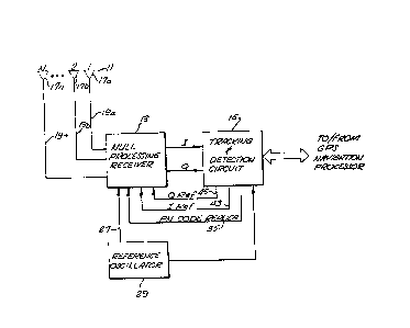
FIG. 1 ls a fi~mpllfied block diagram of the receiver
portion of a Global Positioning System (GPS), which includes a
null processing receiver embodying the present inventlon; and
FIG. 2 is a ~implified blocX diagram depicting the
~ultiple antenna elements and the null processing receiver
circuit of FIG. 1.
DESCRIP~ION OF T~r PREFEP.P.ED EM~ODIMENT
With reference now to the drawings, and particularly to
FIG. 1, there is ~hown a simplified bloc~ diagram of a portion
of a Global Positioning System (GPS) that receives a num~er of
~odulated rf signals from an antenna array 11 and detects one or
~ore binary codes originally transmitted from a corresponding
number of orbiting satellites. The detected codes are supplied
to a GPS navigation processor, which processes the codes to
determine the receiver's precise geographic location. ~he
~odulated signals received from the antenna array can sometimes
contain interference in the form of a ja~ming signal. A null
processing receiver 13 and tracP.ing and detection circuit 15
suitably processes the modulated signals to substantially
eliminate this interference from the codes supplied to the GPS
navigation processor.
As shown in FIG. 1, the antenna array 11 includes ~
elements, designated 17a-17n. The modulated antenna signals are
supplied on lines 19a-19n to the null ~rocessing receiver 13,
which demodulates and combines the signals in a prescribed
fashion to produce quad_ature I and Q data signals. These data
- 5 -
2 9
Po3 2209
signals are supplled on lines 21 and 23, respectively, to thetracking and detection circuit 15, which extracts certain
informatlon from the signals and supplies the information to the
GPS navigation processor. ~he tracklng anB detection circult,
which is of conventional design, also generates various
reference signals used by the null processing receiver to
properly demodulate the incoming antenna signals.
In produclng the quadrature I and Q data signals output
on lines 21 and 23, the null processing receiver 13 combines the
various antenna signals togethsr in such a fashion that a strong
lnterference signal ti.e., a ja~ming signal~ contained in the
antenna signals is substantially nulled out. In the past,
receivers of this kind achieved this nulling by a complex
weighting, i.e., amplitude and phase angle adjustment, of the
received antenna signals prior to summation. This has
necessarily re~uired the use of controllably adjustable rf
circuitry for gain and phase matching, which is usually highly
sensitive and difficult to use and adjust.
In accordance with the invention, the null processing
receiver 13 combines the information contained in the antenna
signals received on lines l9a-19n without the need for any
complex weighting of the rf signals. Rather, the receiver
weights the various signals after demodulation and conversion to
digital formats. This greatly simplifies the receiver and
significantly reduces its cost, weight and power consumption.
I~ore particularly, and with reference to ~IG. 2, it
will be observed that the null processing receiver 13 receives
the N antenna signals on lines l9a-19n from the antenna array 11
and outputs on lines 21 and 23 the respective orthogonal I and Q
data signals. In generating these I and Q signals, the receiver
~ 131~52~
P03 2209
removes a spread spectrum pn code and any interference or
~amming signal contained in the original antenna signals. The I
and Q signals actually are substantlally the same as those
produced by prior receivers. The receiver of the invention,
however, produces them in a substanti~lly simpler and more
reliable fashion.
The null processing recei~er 13 contains both a
hardware section and a software section, with a separate,
ldentical hardware channel being provided for each antenna
signal. Addressing first the hardware channel for the antenna
signal supplied on line l9a from the first antenna element 17a,
lt will be observed that the signal is initially connected to a
mixer 25a. A flxed local oscillator signal is also supplied to
the mixer, via line 27 from a reference oscillator 29 (FIG. 1),
to down-convert the antenna signal from L-band to approximately
60 MHz. The down-converted or intermediate-frequency (i. r. )
signal is supplied on line 31a to a second mixer 33a, where it
is multiplied by a locally-generated replica of the modulating
pn code. This replica code, which is generated by the trac~ing
and detection circuit 15 ~FIG. 1), in a conventional fashion, is
supplied to the second mixer on line 35. When the replica code
and the incoming pn code are properly synchronized, the second
mixer essentially strips the code from the modulated signal,
leaving an i.f. carrier signal modulated only by lower data rate
position information. Of course, random noise and any jamming
signal in the same frequency band are superimposed on the
demodulated carrier. The jamming signal can be derived , for
example, from a CW jammer, a broadband jammer, a swept-fm
jam~er, or a pulsed jammer.
- 7 -
2 9
P0~ 2209
The demodulated carrler signal is output by the second
mixer 33a on llne 37a, ~or connectlon to both a third mixer 39a
and a fourth mixer 41a. These latter two ~ixers multlply the
carrier signal ~y orthogonal I and Q reference carrler signals
supplied on lines 43 and 45, respectively, from the tracking and
detection circuit 15 (FIG. 1). These reference signals are
properly synchronized with the incoming carrier, tracking any
doppler shift that might be present, such that the two mixers
provide orthogonal, analog baseband data signals. For this
first channel, these two signals are designated Il and Ql
The respective baseband Il and Ql signals are
suppl~ed on lines 47a and 49a to a pair of low pass filters Sla
and 53a and, in turn, on lines 55a and 57a to a pair of
analog-to-digital converters 59a and 61a. The filtered and
digitized Il and Ql signals are then output on lines 63a and
65a, respectively, for further processing in the software
section of the null processing receiver 13.
As previously mentioned, the modulated antenna signals
supplied on lines l9a-19n from the antenna elements 17a-17n are
each processed in a separate, identical hardware channel. The
channels for the second through nth signals are identical to
that for the first signal, desc.ibed above. The various mixers,
low pass filters, analog-to-digital converters, and signal lines
in each channel are identified by the same reference numerals as
the corresponding elements ~f the first channel, but followed by
letters corresponding to the letter of the antenna signal.
The hardware section of the null processing receiver 13
thus produces n pairs of orthogonal, digiti-ed I and Q data
signals, designated Il-In and Ql~Qn- These data siana!s
- 3 -
.
~311529
Po3 2209
are supplied on lines 63a-63n and 65a-65n, respectively, to the
software section of the receiver.
It will be appreciated that even with the filterins
provided by the low-pass filters 51a-51n and 53a-53n, the
digitized Il and Ql signals will contaln significant
amounts of noise, especially when a jamming signal is being
received. Demodulation of the pn code provides a certain
processing gain (about 40 db~, but even considering this, the
slgnal-to-noise ratio can still be as low as -20 to -30 db. By
weighting the various In and Qn signals and then summing the
weighted signals, the software section of the null processing
receiver 13 effectively eli~inates the jamming signal co~ponent
from the data and thereby improves the signal-to-noise ratio to
about +10 to +20 db. By perfcrning the nulling function after
demodulation, the 40 db of processing gain sharply reduces the
required dynamic range.
The digitized In and Qn signals supplied on lines
63a-63n and 65a-65n, respectively, are further processed in a
microprocessor, whose function is depicted schematically in the
software section of the block diagram of FIG. 2. The func~ion
is depicted using conventional hardware elements, for ease of
understanding. Those of ordinary s~ill in the art will be
readily capable of implementing these equivalent hardware
functions in a microprocessor.
More particularly, it will be okserved that the
software section of the block diagram of FIG. 2 can be divided
into two identical sections. The upper section includes a
summer 67 for producing a digital InUll signal in which the
jamming signal has been nulled out, and the bottom sec_ion
includes a su~er 69 for producing an ortho?onal Qnull signal
_ g _
~3~29
P03 2209
in which the ~amming signal likewise has been nulled out.
Basically, each such section sums one digitized data s~ynal
derived from the ~irst antenna element 17a wlth weighted
versions nf all of the digitized data signals derived from the
remaining antenna elements 17b-17n. The former, non-weighted
signlls (i.e., Il and Ql) can be termed prlmary informatlon
signals, and the latter, welghted signals (l.e., I2-In and
Q2~Qn) can be termed auxiliary information signals.
The weighted signals supplied to the summer 67 are
produced by weighting networks 70I2~70In and 7Q2 72Qn
slmilarly, the weighted signals supplied to the summer 69 are
produced by weighting netwsrks 72I2-72In and 72Q2 72Qn-
These networks ~ultlply each of the 2n-2 auxiliary signals by
predetermined dc weighting signals, which are generated by
correlating the auxiliary signals with the summer output
signals, i.e., the InUll signal on line 21 and the Qnull
signal on line 23.
Thus, the weighting network 70I2 for the I2 channel
of the upper (i.e., InUll) section includes a mixer 71I2 for
multiplying together the I2 auxiliary signal supplied on line
63b and the InUll signal supplied on line 21. The resulting
product is supplied on line 73I2 to a negative integrator
75I2~ which integrates the signal to produce a dc weighting
signal output on line 77I2. A multiplier 79I2 multiplies
this weighting signal by the I2 auxiliary signal, to produce
the weighted or intermediate signal. The latter is output by
the network 70I2 on line 81I2 for coupling to the su~mer 67,
which sums it with the Il primary signal and the weighted
signals for the remaining auxiliary sisnal channels, to produ_e
the In~.ll si5nal-
-- 10 --
~ 13~ i29
- P03 2209
A corresponding ~ixer, negative lntegrator and
uultiplier for each of the remaining weigh~ing networks
70I3-70In and 7Q2~7Qn provide corresponding weighted
6ignals for each auxilliary channel. Shus, 2n-2 sets o~
elements are required to produce the InUll signal. In FIG. 2,
only the elements for the I2, Q2 and Qn channels are
shown.
~ he lower (i.e., Qnull) section of the right side of
FIG.- 2 is identical to the upper (i.e., Inull) section~ except
that the Ql pri~ary -ignal on l~ne 65a is substituted for the
Il pr~mary signal on l~ne 63a. Thus, the su~mer 69 sums
together the Ql primary signal with prescr.~ed weighted
signals for each of the auxiliary channels (i.e., I2-In and
Q2~Qn). In the specific ca~e of the I2 channel, the
weighting network 72I2 includes a mixer 83I2 for multiplying
together the I2 auxiliary signal and Qnull signal, supplied
on lines 63b and 23, respectively, to produce a product signal.
An integrator 85I2 receives this product signal on line 87I2
and integrates it to produce a weighting signal that is then
supplied on line 89I2 to a multiplier 91I2, which
appropriately weights the I2 signal. The resulting weiyhted
signal is supplied on line 93I2 to the summer 69.
Corresponding elements are provided for all of the auxiliary
channels, FIG. 2 depicting only the I2, Q2 and Qn
channels.
Operation of the software portion of the null
processing receiver 13 will be better understood with _eference
to a particular example, in which a jarming signal is present in
the Il and Q1 primary signals and in all of the I2-In
and Q2~Qn auxiliary signals. If, for exa.ple, all n antenna
-- 11 --
1 3 1 1 ~ ~ 9
P03 2209
elements 17a-17n are coplanar and the jamming signal ls received
from a direction normal to that plane and lf the cable lengths
and phase delays in the various channels all correspond exactly,
then all of the I channel signals are equal to each other an~
all of the Q channel signals are equal to each other. In
addltion, the I channel signals are all uncorrelated with, ~.e.,
orthogonal to, the Q channel signals. If we assume that the
various weightlng signals produced by the integrators
75I2~75In are all ~nitially zero, then all of the weighted
signals will likewise be zero and the InUll signal will be
identical to the Il signal. Since the InUll and I2
signals will then both contain the jamming signal, the product
signal output by the mixer 71I2 will be positive and the
negative integrator 75I2 will begin ramping negatively. The
multiplier 79I2 therefore produces a weighted signal that is
the inverse of the I2 auxiliary signal, progressively
increasing in amplitude. The same progression occurs in the
remaining In channels, because the jamming signal is similarly
present in the auxiliary signals for those channels. The
weighted signals for the Q2~Qn channels will remain at ~ero,
because the auxiliary signals for these channels are
uncorrelated with the InUll signal.
~ ventually, contributions of the weighted signals will
cancel out the jamming signal component of the Il primary
signal such that it is completely eliminated from the In
signal. When this occurs, the InUll signal will be
uncorrelated with all of the auxiliary signals and the various
mixers 71I2-71In will all produce product sisnals that are
essentially zero. The weighting signals produced by the
corresponding negative integrators 75I2~75In will therefore
remain fixed at their current levels.
- 12 -
13~52~
P03 2209
The same process ls followed in the Qnull section ofthe null processing receiver 13. That is, the weightlng of the
auxiliary signals is controllably adjusted until the Qnull
section is uncorrelated with each of the I2-In and Q2~Qn
auxiliary signals.
It should be noted that if the respective phase angles
of the local oscillator signal or I and ~ reference signals
applied to the various channels are different ~due to cable
length variations, etc.), then the resulting magnitudes of the
jam~ing signal components of the Il-In and Ql~Qn signals
also will be different. This has no effect on the receiver's
performance, however, because the feedback control provided by
the software implemented in the microprocessor will
automatically correct for this. In addition, weighting could be
provided for the Il and Ql siynals; as well, with no real
effect on the receiver's performance.
The separate elements 17a-17n of the antenna ar~ay 11
are arran~ed with respect to each other such that they p-ovide a
predetermined spatial gain, with a known pattern of lobes and
nulls. That is, the antenna array's gain varies as a func~ion
of direction, with a substantially reduced gain occurrir.g in
particular directions. The weighting process performed by the
microprocessor actually adjusts the antenna null pattern to
align a given null or low-gain direction with the detected
source of a jamming signal.
The receiver apparatus automatically nulls out a
plurality of independent jamming signals. In particular, for an
appara~us used with N antenna elements, up to ~-1 separate
jamming signals can be nulled out. The N-l spatial nulls are
- 13 -
~ 1311~29
~03 2209
all lndependently steerable, to track any rel~tlve movement of
the sources of the jamming signals.
In situations where the direction to the source of the
~amming ~ignal contlnuDusly Yaries, the weighting of the various
slgnals must vary correspondingly. ~he microprocessor must
update the correlation between the Inull and Qnull cignals
and the various auxiliary information signaln at a rate
sufficiently fast to enable tracking of the jamming source
direction.
As previously mentioned, the null processing receiver
13 operates to null out the strongest signal received within the
frequency band of interest. This operating mode ls desirable,
because when a ja~ming signal is present it is ordinarily many
times stronger than the satellite signal to be detected. When a
~amming signal is not present, however, care must be taken to
ensure that the receive~ does not null out the desired satellite
signal.
Preventing the nulling of the desired satellite signal
is re~uired only when the signal-to-noise ratio exceeds 0 db and
no higher powered jamming signal is present. This can
effectively be ensured by periodically substituting a
non-replica of the incoming pn code, i.e., a bogey code, for the
replica code ordinarily supplied to the receiver 13 on line 35.
Each hardware channel therefore will be unable to properly
demodulate the incoming signal and there is no risk that the
receiver will inadvertently null it out. This periodic
substitution of a non-replica code is preferably per~ormed at a
duty cycle of, for example, 50 percent. During alterna~e
intervals, when the pn code replica is being supplied, the
InUll and Qnull signals output by the receiver 13 on lines
.
P ~ 311529
Po3 2209
21 and 23, respectlvely, will contaln the desired ~atelllte
data.
The ~icroprocessor whose function is represented by the
hardware-equivalent elements depicted on the rlght side of FIG.
2 lnherently i~plements a least mean-square error algorith~.
~his algorithm minimizes the power level of the InUll and
Qnull signals. It will be appreciated that alternative
schemes for weighting the various auxiliary signals can also be
utilized. In addition, it will be appreciated that low-pass
filters can be substituted for ~he integrators 75I2~75Qn and
85I2-85Qn~ without a significant effect on performance, and
that a dithering process can be substituted for the correlation
process performed by the mixers 71I2-71Qn and 83I2-83Qn~
As an alternative to the multiple feedback loops
present ln the software section of FIG. 2, the InUll and
Qnull signals could be produced using computational techniques
such as direct ~atrix inversion. Such techniques could minimize
output power, and thus null out any jamming signals, simply by
appropriately correlating the various auxiliary information
signals.
It should be appreciated from the foregoing desc-iption
that the present invention provides an improved null processing
receiver apparatus that effectively nulls out an rf interference
signal without the need for any complex weighting of rf
signals. A plurality of L-band antenna signals are down
converted, demodulated to baseband, and converted to
corresponding digital signals in separate channels. The digital
signals are then appropriately weighted and summed in such a
fashion as to minimize output power and, thereby, null out any
undesired interference signal.
- 15 -
~3~1 529
po3 2209
~ ltho~gh the present lnvention has been described in
detail with reference to the presently preferred embodlment,
those of ordinary sklll in the ~rt will appreciate that various
modifications can be made without departing from the lnventlon.
Accordlngly, the inventlon ls deflned only by the following
clai~s.