Note: Descriptions are shown in the official language in which they were submitted.
I /7L~ 6 5 /n~lcS~
- - 1 J I 1 553
TO ALL WHOM IT MAY CONCERN:
BE IT KNOWN THAT I, Melvyn McGann, a British subject
residing at 32 Queens Road, Chelmsford, Essex, England,
have invented a certain new and useful
LINEARITY ADJUSTING CIRC~IT
of which the following is a Specification:-
Background of the Invention
This invention relates to a linearity-adjusting
circuit for adjusting, usually correcting, the rate of
change of amplitude of an output signal with respect to
the amplitude of an input signal from which the output
signal is derived. In most applications, the output
signal amplitude is nominally proportional to the input
signal amplitude. The invention is particularly useful,
for example, in a high frequency pre-distortion circuit
for signals which are to undergo amplification in power
amplifiers, such as klystrons which are used in
television transmission. Klystrons, and indeed many high
power amplifiers and the like, introduce undesirable
signal distortions, and a linearity-correcting circuit is
required for ensuring a linear amplitude relationship
between the envelope of the modulated and power-amplified
transmission signal and the video input signal which was
used in the initial modulation process.
In some existing colour television transmitter
- 2 - ~J~ 1 5 53
chains, an appropriate pre-distortion is introduced into
the intermediate frequency signal before the waveband-
dependant radio frequency stage, for linearity correction.
To obtain the correct amount of pre-distortion over the
full amplitude range, variable impedances or other
elements of the pre-distortion circuit are adjusted
manually until the envelope of the transmitted signal has
a sufficiently linear relationship with the envelope of
the input modulated signal, over the entire range of
envelope amplitudes. Since the characteristics of the
transmitter chain vary in operation with supply voltage
levels and ambient temperature amongst other things, it is
found that re-adjustment of the~circuit elements is
necessary quite frequently. If the non-linearity occurs
only over a narrow band of amplitudes, it is found that
adjustment of just one circuit element may be sufficient
to correct this particular non-linearity, but that it then
introduces non-linearities at other amplitude levels.
Consequently, even for a slight correction, it is
necessary to adjust more than one of the circuit elements.
Moreover, because of the interdependence of the settings
of the circuit elements, they frequently require more than
one adjustment to compensate for each change in power-
amplifier characteristics, considerable skill and
experience is required in order to judge the degree of
adjustrnent required.
i .~ J 5 ~
Summary of the Invention
The purpose of the present invention is to provide a
linearity-adjusting circuit which is capable of aut~matic
control, i.e. without the need for manual adjustment, such
a circuit may then be used in a transmitter chain under
microprocessor control, in response to an automatic and
periodic monitoring of the transmitted signal resulting
from test signals. It was considered that, with existing
hardware, any software solutiGn to the problem would
require a substantial comput'ng capability to implement,
and that changes in the hardware might render the software
solution much simpler.
The invention provides a linearity-adjusting circuit for
adjusting the rate of change of amplitude of an output signal
with respect to the amplitude of an input signal from which
the output signal is derived, comprising, for each of several
bands of the input signal amplitude: means for selectively
introducing a differential voltage to the output signal
amplitude over that amplitude band, such that the mean rate of
changé of amplitude of the output signal with respect to the
amplitude of the input signal is changed accordingly only over
that amplitude band; means for amplifying the input signal to
derive the output signal, the differential voltage introducing
means being coupled to the amplifying means for adjustment of
the gain of the amplifying means as a function of the input
signal amplitude; and control means coupled to the
differential voltage introducing means for selecting over
which amplitude bands to introduce such differential voltages
1 ~ 1 1 553
- 3a -
and for determining the magnitudes of such differential
voltages, to achieve a predetermined linearity variation for
the whole amplitude range, the differential voltage
introducing means comprising a plurality o~ adjustable
constant current sources each arranged to introdu~e to the
amplifying means a differential current at a predetermined
respective input signal amplitude.
- 4 - ~ 553
The invention enables the gain of any amplitude band
of a transmitter chain to be adjusted (usually by way of
correction) independently of the other amplitude bands, so
that the variation of gain in that amplitude band does not
itself introduce gain variations in other amplitude bands
which would then require correction also. This
independent treatment of the various amplitude bands
allows the said control means to be automated much more
simply, and it may for example comprise a microprocessor
control unit.
In another aspect, the invention provides a
transmitter chain comprising a linearity-correcting
circuit according to the first aspect of the invention
described above, means for detecting the amplitude of the
transmitted signal, and control means responsive to the
said detecting means for setting the levels of the said
differential voltages so as to introduce an appropriate
pre-distortion to correct the linearity. In use, colour
television transmitters, for example, transmit an inserted
test signal, in each frame, modulated with an envelope in
the form of a staircase. Using such a test signal, the
detecting means of this aspect of the invention
demodulates and then differentiates the staircase signal
to provide a series of narrow pulses whose heights are
nominally equal. The heights of the pulses are compared
with a predetermined value representing the height they
should be for correct linearity at that particular
~ 71 1553
amplitude band. In response to this comparison, the
control means sets the level or levels of differential
voltage required for correction over the or each
respective amplitude band. The linearity-adjusting
circuit thus compensates for the detected non-linearity by
introducing the appropriate pre-distortion. Such
corrections may be carried out regularly and frequently,
so that the transmitter chain is capable of responding
quickly to changes in the characteristics of the
transmitter due to temperature or supply voltage
fluctuations.
. ~. .
Two ways in which the invention may be performed will
now be described, by way of example only, with reference
to the accompanying drawings.
Brief Description of the Drawings
Figure 1 is a circuit diagram of a linearity-
correcting circuit embodying the invention;
Figure 2 illustrates the amplitude envelope of a
staircase test signal in a colour television transmission,
Figure 3 illustrates the differential, with respect
to time, of a portion of the demodulated test signal of
Figure 2,
Figure 4 is a graph of output amplitude against input
amplitude for the circuit of Figure 1, and
Figure 5 is a circuit diagram of a further linearity-
correcting circuit embodying the invention.
- 6 - 1 Jl 1 5 5 3
Detailed Description of Preferred Embodiments
The linearity-correcting circuit of Figure 1 forms
part of an intermediate frequency corrector unit in a
colour television transmission chain. In this example,
the colour video signal is used to modulate a 38.9 MHz
carrier signal using amplitude modulation. The amplitude-
modulated signal is filtered in a vestigial side band
filter and then pre-distorted in the intermediate
frequency corrector unit to compensate for the distortions
which are anticipated to occur in the later stages of the
transmission chain. The corrected signal is then mixed
with a carrier wave from a heterodyne oscillator to
produce an RF signal which is amplified and then delivered
to a power amplifier, for example a klystron, for
transmission from an antenna at, for example, 40 kW.
The intermediate frequency corrector unit, operating
at intermediate frequency, remains band-independent and
channel-independent, and consequently the same correction
circuits can be used in many different applications. The
intermediate frequency corrector unit includes circuits
which compensate for differential phase distortion and
differential gain distortion, which are described for
example in our UK Patent No. 2153173 and our US Patent No.
4604589, but which are not illustrated or described in the
present specification.
With reference to Figure 1, the vision intermediate
frequency signal, at an amplitude Vin, is input to a
1 5~jJ
linearity-correcting circuit, whose output amplitude VOut,
having undergone a pre-distortion appropriate for the
required linearity correction, is provided to other
correction ciruits of the intermediate frequency corrector
unit.
The input voltage Vin is applied to the base of a
transistor TRl whose collector is connected to a +12 volts
supply by way of a transformer T whose other winding
provides the output signal VOut. The emitter of
transistor TRl is connected to a -12 volts supply
potential by way of an inductance Ll and resistance Rl,
for D.C. biasing, and to earth by way of a blocking
capacitor Cl and a gain-control resistor Rg.
Several, in this case five, alternative current paths
between the emitter of transistor TRl and the -12 volts
supply are provided in parallel by an array 11 of current
sources Il to I5 controlled by an array 10 of diodes.
Each current source Il (I2, I3, I4, I5) is connected via a
corresponding diode Dll (D21, D31, D41, D51) to a
corresponding different supply potential Vl (V2, V3, V4,
V5); and also to the emitter of transistor TRl via a
respective diode Dl (D2, D3, D4, D5) whose polarity is
reversed with respect to the first-mentioned diode. The
supply potentials Vl to V5 form a regular series of
increasing levels, selected in accordance with levels of
the staircase steps of an inserted test signal (described
below), and in this example are respectively 7.1 volts,
1 5 5 3
8 -
8.1 volts, 9.1 volts, 10.1 volts and 11.1 volts. The
centre level VO is 6.0 volts.
Current source Il draws current through diode Dll
when the transistor emitter voltage is lower than Vl, but
through diode Dl when the emitter voltage is above Vl.
The other current sources I2 to I5 operate in a similar
manner; thus, when the emitter voltage exceeds V5, all
five current sources draw current from the transistor
emitter. The current il (i2, i3, i4, i5) provided by the
respective current source Il (I2, I3, I4, I5) is
effectively added to the transistor collector current Ic,
which in turn determines the amplitude of the output
signal VOut. Thus pre-distortions are introduced in
discrete steps over 5 amplitude bands. The current
sources Il to I5 are all independently variable, either
manually or, preferably, under microprocessor control, in
response to the varying amplitude characteristic of the
transmission signal provided by the power amplifier, to
provide the correct levels of pre-distortion to compensate
for the distortion in the power amplifier.
Colour television transmissions conventionally
include an inserted test transmission (mentioned above)
comprising a synchronisation pulse followed by a
staircase, one in every field of the transmitted signal,
as shown in Figure 2. The staircase portion comprises six
amplitude levels joined by nearly vertical slope portions
1,~t553
g
Sl, S2, S3, S4 and S5 respectively, whose mid-points have
potentials Vl, V2, V3, V4 and VS. These slope portions
are nominally of the same gradient and height. The colour
subcarriers are not shown. This test transmission is used
to monitor the lineari~y of the transmitter chain by
observing the effect of the power amplifier on the slopes
Sl to S5 of the test signal. The slopes vary in
proportion to the change in the rate of change of output
amplitude with input amplitude, i.e. they represent the
degree of non-linearity, at the relevant amplitude band~
This monitoring is conventionally performed by feeding
back the transmission signal, either from the power
amplifier output or from a television receiver, to a
control circuit which demodulates and then differentiates,
with respect to time, the staircase portion of the test
signal, the result of which is shown in Figure 3. In
Figure 3, peaks Pl to P5 correspond respectively to slopes
Sl to S5, and are nominally of the same height H.
Distortion in the power amplifier is manifested by a
deviation of one or more of these peaks from the expected
height H: in Figure 3, peaks P3, P4 and P5 are slightly
lower than the expected level H, indicating that a pre-
distortion is required in the linearity-correcting circuit
of the transmitter chain.
The linearity-correcting circuit of Figure 1 is
capable of correcting for non-linearity over any one of
the five voltage bands centred at Vl, V2, etc.,
-10~ lJtl553
independently of all the other voltage bands, simply by
varying the corresponding current source independently of
the other current sources in the bank 11 of current
sources. Firstly, the circuit detects the levels of the
steps of the staircase, computes the mid-slope levels Vl
to V5, and then sets the supply potentials of the diode
bank 10 accordingly. Then in order to correct the
linearity over the voltage band centred at V3, for
example, the peak P3 is compared with the nominal level H,
and the current source I3 is adjusted in accordance with
the difference, in a direction such as to minimise that
difference. In this example, peak P3 is too low, and
accordingly the current i3 of current source I3 is
increased accordingly. Subsequent test signals are again
monitored, and the whole process repeated; any residual
error in the height of peak P3 is again corrected by a
further change in current source I3.
The effect of such a correction on the output
amplitude VOut for the expected range of input amplitudes
Vin is illustrated diagrammatically in Figure 4. It is
assumed, in the example of Figure 4, that the transmitter
chain is perfectly linear over most input voltages, as
represented by portions cl and C3 of the graph. By
increasing the current source I3, however, the slope c2 of
the graph near input voltage V3 is increased, so as to
introduce the appropriate amount of pre-distortion. It
11 - t~1553
will be appreciated that the width Vw of the band over
which the slope c2 is changed need not necessarily be
equal to the difference between the steps of the staircase
adjacent voltage V3, so long as the mean rate of change of
voltage is changed appropriately over that band; the value
of Vw will depend on the forward drop of the diodes D3 and
D31. The nominal slope cl is determined by the value of
the resistor Rg. The value of the increase Vi in output
voltage caused by the adjustment is determined by the
current i3 and the effective A.C. load seen by the
collector of TRI, which is set by the load on the
transformer and its turns ratio.
In existing linearity-correcting circuits which do
not employ current sources for individual voltage bands,
the slope in Figure 4 for the higher voltage bands would
also vary as a result of the adjustment made for the band
centred at V3, and the slope C3 might instead be the slope
C'3 as shown in broken lines. This would then necessitate
corresponding corrections for input voltages centred at V4
and above.
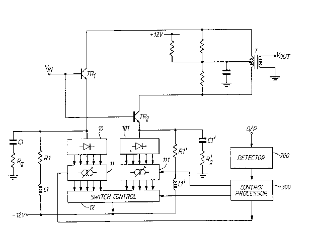
The second, and preferred embodiment of the invention
will now be described with reference to Figure 5. The
linearity-correcting circuit of Figure 5 comprises two
circuits of the type shown in Figure 1, and similar parts
are given the same reference numerals.
The transistor TRl, diode bank 10 and current source
array 11, resistor Rg, resistance Rl and inductance Ll are
- 12 - t J t ~ 5 5 3
the same as the corresponding components of the circuit of
Figure 1. A similar second circuit, comprising transistor
TR2, diode bank 101, current source array 111, bias
resistor Rlg, resistance R'l and inductance L'l, is
connected in parallel. The collectors of the two
transistors are connected across the output transformer T,
to which the +12 volts supply is connected at a central
tapping point. The current sources are switched
individually in a switch control unit 12 such that, for
each of the 5 amplitude bands, the appropriate current
source in either array 11 or array 111, but not both, is
connected to the -12 volts level.
A detector 200 receives an output signal from the
power amplifier and processes the signal to determine the
amplitude envelope resulting from the staircase portion of
the test transmissions. This amplitude envelope is then
fed to a control processor 300 which differentiates the
envelope to derive the levels of the peaks P12 to P56
(Figure 3), and to determine what changes are required to
one or more of the currents "injected" by the current
sources.
The current sources, in this example, are high
resistances, of 18 kilo-ohms, connected to variable
voltage sources, but alternatives would be active constant
current circuits in series with chokes. The switch
control unit 12 is a diagrammatic representation of the
- 13 - 1311553
switching function, and in practice the switches are
integrated with the current source arrays 11, 111. The
diodes require rapid speed of operation and low forward
drop, and in this example are hot carrier diodes;
alternatively, however, they could be silicon diodes.
The two transistors TRl and TR2 are driven such that
the output voltage VOut depends on the difference between
their collector currents by subtraction in the transformer
T. This enables either positive or negative changes in
the slopes to be made: the circuit of Figure 1 alone is
not capable of reducing the slopes, i.e. reducing the
rates of change of output voltage with input voltage. The
magnitude of the change is determined, as before, by
adjustment of the appropriate current source, by means of
a signal from the control processor 300. The direction of
the change is determined by switching on the appropriate
current source either in bank 11 or in bank 111, using
control signals sent to the switch control unit 12 from
the control processor 300.
A further advantage of the circuit of Figure 5,
compared with that of Figure 1, is that the effect of
stray capacitance at the transistor emitters is reduced by
the way in which the two transistor circuits are connected
in anti-phase. Stray capacitance in the circuit of Figure
1 reduces the independence between the effects of the
adjustment of the different current sources. Stray
capacitance could be reduced further by integrating the
- 14 _ t 1 1553
whole linearity-correcting circuit on one chip.
The linearity-correcting circuits of Figures 1 and 5
do not require the base~and component of the input signal
to be divided out, as is the case with many existing such
circuits, but rather receives the intermediate frequency
component and responds to its amplitude envelope.
However, these clrcuits embodying the invention are still
capable of operating at lower input signal frequencies,
e.g. at video frequency or even down to D.C. (provided
that a resistance were used in place of the transformer
T).
Although the invention has been illustrated in the
context of television transmission, it has many other
5~
applications. The invention may be used for linearity
correction in any system whose output is nominally
proportional to the input for a range of input amplitudes,
and is not limited to amplitude-modulated carrier signals.
The invention could, for example, be used in direct-
current amplification, where a D.C. output signal
potential is nominally proportional to that of a D.C.
input signal.
Further, although the invention has been illustrated
in the form of a linearity-correcting circuit, the
invention could be embodied in a circuit for test purposes
which deliberately introduces linearity distortion into a
signal, for example to simulate a particular power-
- 15 - t~ 553
amplifier. Indeed, the principle of the invention is
applicable to circuits in which the output amplitude is
not necessarily nominally proportional to the input
amplitude, for example circuits for synthesising any
desired gain-amplitude profile.