Note: Descriptions are shown in the official language in which they were submitted.
-`; 1 31 1 845
27252/NSCO-15
02J06/89:APP:efd
S MULTISTEP FLAS~ ANALOG TO DIGITAL
CONVERTER WITH VOLTAGE ESTIMATOR
INTRODUCTION
This invention pertains to analog to digital
converters, and more particularly to flash analog to
digital converters wherein a plurality of comparisons
between a signal related to the input signal and
reference signals are made in order to provide a
plurality of bits of the digital word simultaneously.
Analog to digital converters are well known in
the prior art. One form of analog to digital converter
utilizes successive approximation in order to use a
single comparator to successively compare an input
signal to one of a plurality of reference voltages.
While this type of analog to digital convertor is
widely used, and is relatively inexpensive because it
uses only a single comparator, it is inherently rather
slow since a number of comparisons must be made in
order to convert each analog sample into a digital
output word. One example of such a successive
approximation analog to digital converter is described
in U.S. Patent No. 4,691,190.
Another type of analog to digital convertor is
the so-called "flash" converter which includes a
plurality of comparators which simultaneously compare
the input signal to an associated one of a plurality of
reference signals in order to simultaneously provide a
plurality of output bits of the digital output word.
One example of such a flash analog to digital converter
is shown in U.S. Patent No. 4,608,555. Such a flash
" t31 184~
2 72094-70
converter requires 2N comparators in order to provide an N bit
output word. Thus, for a 10-bit analog to digital converter, 1024
comparators are needed.
Another type of flash analog to digital converter is the
half flash analog to digital converter described in U.S. Patent
No. 4,639,715. A half flash analog to digital converter generates
high and low order bits of the digital output word in sequence by
two flash conversion cycles per analog input sample. The prior
art half flash analog to digital converter requires only 2 x 2N/2
comparators. Thus, for a 10-bit analog to digital converter, 64
comparators are needed. However, the speed of an analog to
digital conversion performed by this type of flash analog to
digital converter is approximately one half that of the prior art
flash analog to digital converter which generates all bits of the
digital output word simultaneously, as described in the
aforementioned U.S. Patent No. 4,608,555.
SUHMARY
In accordance with teachings of this invention, a novel
multistep flash analog to digital converter is taught. This
multistep analog to digital converter includes a voltage estimator
which quickly provides a rough estimate of the analog input
signal. This rough estimate is used to select appropriate
reference voltage tap points for use in the first flash
conversion. This first flash conversion, together with the
voltage estimate, provides the most significant bits of the
digital output word. A digital to analog converter is used to
provide a residual voltage which is then converted by a second
1 31 1~45
3 72094-70
the flash converter, thereby providing the least significant bits
of the digital output word.
In accordance with the teachings of this invention,
significantly fewer components are required, thereby reducing
circuit complexity, cost, and power consumption. In one
embodiment of this invention, the voltage estimate is performed at
the same time that the analog input signal is sampled by the flash
converter in preparation for the first flash conversion.
Therefore, speed of operation is not degraded by the addition of
the voltage estimator.
According to a broad aspect of the invention there is
provided an N bit multistep flash analog to digital converter
comprising:
an input terminal for receiving an analog input signal;
an output bus for providing an N bit digital word
representing the magnitude of said input signal;
an analog signal estimator having an lnput lead coupled to
said lnput termlnal and an output bus for providlng an M blt
estlmator word representing an approximate magnltude of said
0 analog input signal;
a P bit flash converter having an input lead for receiving an
analog signal to be converted and an output bus for providing a P
bit digital word representing the magnitude of said analog signal
applied to said input lead of said flash converter;
means for providing a residual analog signal equal to said
input analog signal minus the analog equivalent of said M bit
estimator word and a P bit digital word from a first cycle of said
P bit flash converter;
1 31 ~ 845
4 72094-70
switch means for coupling said input lead of said P bit flash
converter to receive said analog input signal during a first cycle
of said P bit flash converter and to receive said residual analog
signal during a second cycle of said P bit flash converter; and
means for combining said M bit estimator word and said P bit
digital words resulting from said first and second cycles of said
P bit flash converter in order to provide said N bit digital
output word.
BRIEF DESCRIPTION OF THE DRAWINGS
Figure 1 is a diagram of a typical prior art half flash
analog to digital converter;
Figure 2 is a block diagram of one embodiment of a
multistep flash analog to digital converter constructed in
accordance with the teachings of this invention;
Figure 3 is a more detalled diagram depicting the
embodiment of Figure 2;
Flgure 4 is a schematic diagram depicting one embodiment
of a comparator suitable for use in conjunction with the teachings
of this invention;
Figure S depicts timing waveforms associated with the
circuit of Figure 4; and
Figure 6 is a schematic diagram of one embodiment of a
sense ampllfier suitable for use in accordance with the teachings
; of this invention.
DETAILED DhSCRIPTION
A typical N bit half flash analog to digital converter
is shown in the schematic diagram of Eigure 1. This converter
utilizes two N/2 bit flash converters 10 and 13 and a single N/2
131 1845
4a 72094-70
bit digital to analog converter 11. The analog input signal i5
received on input terminal 15 and is first converted by flash
converter 10 to provide N/2 bits of the digital output word.
These N~2 bits are also fed to digital to analog converter 11
which provides an analog signal which is subtracted from the input
signal by summing means 12. The result of this subtraction is a
residual voltage which is then converted by second N/2 bit flash
converter 13 in order to provide the remaining N/2 bits of the N
bit output word.
Figure 2 is a block diagram of one embodiment of a 10-
bit multistep flash analog to digital converter constructed in
accordance with the teachings of this invention which provides a
10-bit digital word on output bus 28 in response to a sample of an
input voltage Vin which is received on input terminal 21. In
accordance with the teachings of this invention, a key element is
3-bit voltage estimator 22 which provides a rough approximation of
input voltage Vin. A single 4-bit flash converter 23 is used for
both conversion cycles requlred to convert an analog input voltage
Vln to a digital output word.
Referring to Eigure 2, at the beginning of an analog to
digital conversion, analog input signal Vin received on input
terminal 21 is evaluated by voltage estimator 22 and, at the same
time, is sampled by operation of switch 24 on the input of 4-bit
flash converter 23. Based upon the result of the operation of
voltage estimator 22, appropriate tap points within 4-bit flash
converter 23 are selected, and the first 4-bit flash conversion is
performed. The three bits provided by voltage estimator 22 and
the four bits provided by the first cycle of 4-bit flash converter
131 1845
4b 72094-70
23 are applied to decoder/digital correction circuit 27, which in
turn provides the six most significant bits of the digital output
word made available on output bus 28.
After the first conversion, digital to analog converter
25 receives the three bits from voltage estimator 23 and the four
bits from the first cycle of 4-bit flash converter 23 and
generates an intermediate analog signal which is applled to analog
summing means
131 1845
26. This intermediate analog signal is subtracted by
analog summing means 26 from input voltage Vin, and the
resulting analog signal is applied by switch 24 to 4-
bit flash converter 23 for conversion during the second
cycle of conversion. Appropriate reference voltages
are selected by 4-bit flash convertor 23 and the
resulting analog signal from analog summing means 26 is
converted by 4-bit flash convertor 23. The 4-bit
digital word provided by the second cycle of converter
23 serves as the four least significant bits of the
digital output word available on output bus 28.
Since the voltage estimation is done
simultaneously when analog input signal Vin is sampled
by 4-bit flash converter 23, the overall conversion
speed is not slowed down by the addition of voltage
estimator 22. Therefore, an analog to digital
converter construced in accordance with the teachings
of this invention has the same speed as a prior art
half flash analog to digital converter. Due to the
inclusion of 3-bit voltage estimator 22, the resolution
requirement for the flash converter is reduced from N/2
bits to only (N/2)-1 bits. For a 10-bit analog to
digital converter, only 16 comparators are needed in
the flash converter, and only six sense amplifiers are
needed in the voltage estimator. Therefore, a reduced
number of components are required as compared with a
prior art half flash analog to digital converter
providing output words having the same number of bits,
thereby reducing integrated circuit die size, which in
turn decreases cost. Furthermore, with a decrease in
components, power consumption is reduced compared with
prior art half flash analog to digital converters.
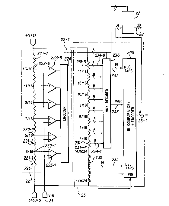
Figure 3 is a schematic diagram of one embodi-
ment of 3-bit voltage estimator 22 and 4-bit flash
convertor 23. As shown in Figure 3, voltage estimator
22 includes resistor ladder 221 formed of resistors
221-1 through 221-7 connected between positive and
-`~" 131 1845
reference voltage VREF and ground, respectively. This
resistor ladder has a plurality of taps 222-1 through
222-6 which are connected to one input lead of voltage
sense amplifiers 223-1 through 223-6, respectively.
The other input leads of voltage sense amplifiers 223-1
through 223-6 are connected in common to input voltage
Vin which is applied to input terminal 21.
In one embodiment of this invention, sense
amplifier provides very high speed while being rather
simple in design and operation. Referring to Figure 6,
sense amplifier 223 is constructed as a cross coupled
latch consisting of P channel devices Ml and M2 and N
channel devices M3 and M4. Sense amplifier 223 is
enabled by the operation of P channel device MS and N
channel device M6 in response to clock signal Taz and
its complement Taz. With clock signal Taz high, input
voltage Vin and reference voltage VREF(tap) ~from an
appropriate tap of resistor ladder 221, Fig. 3) are
sampled on input/output nodes 61 and 62, respec-
tively. Taz then goes low isolating Yin and VREF(tap)from nodes 61 and 62, respectively, and turning on
devices M5 and M6, thus enabling sense amplifier 223.
This causes the latch formed of devices Ml through M4
to switch to one of two states, depending on whether
Vin or VREF(tap) as sampled on nodes 61 and 62,
respectively, is greater. Output signals are then
available on input/output nodes 61 and 62. The
response time of sense amplifier 223 is, in one
embodiment, less than 5 nanoseconds.
Referring again to Figure 3, the voltages
available at nodes 222-1 through 222-6 are equal to
2 N) (2N + 1) * VREF ; where (1)
7 131 1845
V(222-N) = the voltage at a selected tap
222-N.
In one embodiment, voltage estimator 22 is
able to provide, within approximately five nanoseconds,
a 3-bit voltage estimator word on bus 22-1 for an input
voltage sample Vin on input terminal 21 ~hich is
simultaneously sampled by flash converter 23. The
accuracy of this 3-bit voltage estimate is not very
critical since taps 222-1 through 222-6 are shifted by
1/16 VREF, in order to overlap the reference voltages
on MS~ resistor ladder 231, as is now described.
Therefore, via digital correction logic 27 (Fig. 2)
error in the voltage estimate as large as 1/16 VREF can
be corrected.
4-bit flash convertor 23 includes most
significant bit ~MSB) resistor ladder 231 including
resistors 231-1 through 231-8 connected in series with
least significant bit (LSB) resistor ladder 232, 16
comparators, and an encoder to provide 4-bits of
resolution. Each resistor 231-1 through 231-8 within
MSB resistor ladder 231 includes eight tap points which
are connected via buses 234-1 through 234-8,
respectively, to multiplexer 236. Thus, a plurality of
eight voltage ranges are applied to multiplexer 236,
and within each of the eight voltage ranges is
contained eight individual voltages. At any given
time, sixteen voltage references are selected by
multiplexer 236 in response to the 3-bit estimator word
applied to multiplexer 236 via bus 22-1. Thus,
multiplexer 236 will select one of seven sets of
sixteen reference voltages each, in response to the 3-
bit estimator word of voltage estimator 22 on bus 22-1,
i.e. those reference voltages contained on buses 234-1
and 234-2; buses 234-2 and 234-3; buses 234-3 and
234-4; buses 234-4 and 234-S; buses 234-5 and 234-6;
buses 234-6 and 234-7; or buses 234-7 and 234-8. The
8 1311845
selected sixteen taps are applied via bus 237 to
comparator and encoder circuitry 240.
To allow for correction of errors in the
digital output word provided by voltage estimator 22,
the tap points of MSB resistor ladder 231 over]ap the
tap points of voltage estimator resistor ladder 221.
Thus, for example, assuming that voltage estimator 22
determines the analog input signal Vin is between 5/16
VREF and 7/16 VREF, multiplexer 236 selects from MSB
resistor ladder 231 the sixteen tap points between 4/16
VREF and 8/16 VREF (i.e. the sixteen tap points of
resistors 231-3 and 231-4). The sixteen tap points are
applied via buses 234-3 and 234-4 to decoder 236 which
in turn selects and applies them via bus 237 to the 16
comparators contained within comparator and encoder
circuit 240. Once these resistor taps are selected,
the first 4-bit flash conversion is performed. Since
the selected 16 taps of MSB resistor ladder 231 provide
a voltage range which extends beyond the range provided
by voltage estimator resistor ladder 221 (1/16 VREF
above and 1/16 VREF below), the errors in the voltage
estimate provided by voltage estimator 22 can be as
large as 1/16 VREF and be corrected. The result of
this first flash conversion, together with the 3-bit
result from voltage estimator 22, are applied to
decoder/digital correction circuitry 27 (Fig. 2) to
provide the six most significant bits of the digital
output word.
After the first flash conversion, the tap
along MSB resistor ladder 231 nearest to but not
greater than (Vin - 1/2 LSB) is selected as voltage
Vdac on lead 238 (Fig. 3). Voltage Vdac is applied to
summing means 26 (Fig. 2) and is subtracted from analog
input voltage Vin. The resulting residual voltage is
applied via switch 24 to 4-bit flash converter 23 which
at this time selects the 16 taps of the LSB resistor
ladder 23 (Fig. 3). The result of this second flash
131 1845
conversion provides the four least significant bits of
the digital ouput word. These four bits of data
combines with the first 6-bits of data in order to
provide the final lQ-bit output word on output bus
23-1.
Figure 4 is a schematic diagram of one embodi-
ment of one of the sixteen comparators contained within
comparator and encoder circuitry 240 (Figure 3). As
shown in Figure 4, a fully differential circuit is
used, providing excellent common mode power supply
rejection. A plurality of input leads are used as
follows. Input lead 401 receives input voltage Vin,
and input lead 402 receives a selected one of the
sixteen voltages selected by multiplexer 236 from MSB
resistor ladder 231 (Figure 3). Input lead 403
receives Vdac from lead 238 (Figure 3), and input lead
404 receives a 1/2 LSB voltage which is obtained, for
example, by using a resistor divider (not shown) to
divide in half the least significant bit voltage
available on the tap closest to ground in LS8 resistor
ladder 232. Input lead 405 receives negative reference
voltage -VREF (e.g. ground), and input lead 406
receives via bus 235 a selected one of the reference
voltages from the 16 tap points of LSB resistor ladder
232 (Figure 3).
The operation of comparator 400 is now
described with reference to the timing diagram of
Figure 5. When Taz is high, comparator 400 is auto
zeroed by closing switches 410-la through 410-3b. In
one embodiment of this invention, this auto zero step
provides an offset error voltage of less than 100
microvolts. With signal Tl high, Vin is applied to
input node 421 and 1/2LSB offset voltage is applied to
input node 422, thus causing comparator 400 to sample
(Vin - 1/2LSB). When Taz goes low (Vin - 1/2LSB) is
held across input capacitors 431 and 432.
Tl then goes low and T2 goes high, applying
lo 131 1845
the MSB tap voltage VMSB to input node 421 and -VREF to
input node 422, thus causing comparator 400 to compare
(Vin - 1/2LSB) with (VMsB ~ (-VREF)),
thereby completing the first flash analog to
ditigal conversion.
T2 then goes low and T3 goes high, connecting
Vdac to input node 421 and VLSB to input node 422,
causing comparator 400 to compare (Vin - 1/2LSB) with
(Vdac - VLSB). This completes the second flash analog
to ditigal conversion.
~ o describe the operation of the embodiment to
Figure 3, two examples are now given with reference to
Table 1. Analog input signal Vin is first evaluated by
voltage estimator 22 and, at the same time, sampled by
comparators 223-1 through 223-6. With analog input
signal Vin around 3.75 volts, voltage estimator 22
determines Vin is within the range of 11/16 VREF to
13/16 VREF. Therefore, the output of encoder 224 is
110. ~his output word selects via multiplexer 236 the
- 20 sixteen taps on MSB resistor ladder which are between
10/16 VRE~ and 14/16 VREF for connection to comparator
array of comparator and encoder 240. A first flash
conversion is now performed resulting in a 4-bit
digital word. For example, when the input signal is
larger than 3.75 volts (for example 3.76 volts), the 4-
bit word resulting from a first flash conversion is
1000. ~he most significant bit of the flash conversion
indicates which one of the two selected resistors of
resistor ladder 231 provides a tap voltage which is
closest to but not greater than (Vin - 1/2 LSB). In
this case, resistor 231-7 is indicated by the logical 1
most significant bit provided by the first flash
conversion. With a logical 1 most significant bit
provided by the first flash conversion, the voltage
estimate word need not be corrected, and correction
circuit 27 selects the uncorrected estimator word (110)
as the three most significant bits of output data and
11 131 1845
the three least significant bits (000) resulting from
the first flash conversion as the next three bits of
ouput data. Thus correction circuit 27 selects 110000
as the six most significant bits of output-data.
On the other hand, when input signal Vin is
less than 3.75 volts (e.g. 3.74 volts), the 4-bit word
provided by the first flash conversion is 0111. The
fact that the most significant bit resulting from the
second flash conversion is a logical 0 means that the
lower (231-6) of the two selected resistors of resistor
ladder 231 provides the reference voltage which is
nearest but not greater than (Vin - 1/2 LSB).
Correction circuit 27 therefore modifies the voltage
estimator data from its original value of 110 to
slightly less by subtracting a logical 1 to provide a
corrected estimator word of 101. Correction circuit 27
thus provides 101111 as the six most significant bits
of output data.
Following the first 4-bit flash conversion,
the four least significant bits are determined by
comparing the sixteen taps on LSB resistor ladder 232
with the residual voltage. As previously described,
the residual voltage is equal to (Vin - Vdac), where
Vdac is the analog value of the four most significant
bits determined by the first flash conversion
operation.
~5
~\
12 1311845
TABLE 1
Example 1 . Example 2
Vref 5 volts 5 volts
-Vref 0 volts 0 volts
Vin 3.76 volts 3.74 volts
estimator 11/16 Vref 11/16 Vref
range to to
13/16 Vref 13/16 Vref
Estimator
output 110 110
MSB taps 10/16 Vref 10/16 Vref
selected to to
14/16 Vref 14/16 Vref
First Flash
Conversion 1000 0111
Corrected
Estimator 110 101
Output
Correction
Circuit Result 110000 10111
Vdac 3.75 volts 3.67185 volts
Residual 0.01 volts 0.06815 volts
voltage
Second Flash 0010 1110
Conversion
10-bit 1100000010 1011111110
output
131 1845
13 72094-70
Although the foregoing invention has been described in
some detail by way of illustration and example for purposes of
clarity of understanding, it will be readily apparent to those of
ordinary skill in the art in light of the teachings of this
invention that certain changes and modifications may be made
thereto without departing from the spirit or scope of the appended
clalms.