Note: Descriptions are shown in the official language in which they were submitted.
1 ~23~9
FIELD OF THE INVENTION
This invention relates to an integrated circuit, low
level, low power, operational amplifier. More particularly, it
relates to an amplifier to the kind above indicated, in which the
necessary supply voltage and power consumption can be reduced and
the phase margin can b~ increased.
B~C GRO~ OF q~ INVENTION
Amplifiers used in small devices, for example hearing
aids, typically have three stages; input, gain and output.
Battery life, size and amplifier size have long been a problem
in these small products. It is desirable to have small
components which will operate with low battery drain and at a low
battery voltage.
Battery life and size have been restricted by the
limited voltage swing capability of typical amplifiers. Usually,
these amplifiers will not operate reliably below 1.5 V with
ground or negative rail sensing capability, or below 1.0 V
without negative ground rail sensing capability.
The typical gain stage requires a relatively large
capacitor for frequency compensation. This can require the
compensation capacitor to be externally connected to the
amplifier integrated circuit. This increases both the size and
cos~ of the amplifier. Additionally, the limited phase margin
caused by the typical gain stage results in limited ranges of
operating configurations beyond which the overall amplifier would
require further e~ternal frequency compensation.
~ '~
:,
~. ;
~23~
-
- 3 -
It is an object of the present invention in
- certain of its aspects variously to increase the common
mode input voltage range and the voltage swing capability
of this type of amplifier, decrease the power consumption,
and increase the available phase margin of the gain stage.
SUliMARY OF THE IIIVEN~ION
In one aspec~, the invention provides for use in
an operational amplifier having a first and a second
supply rail, an output stage, the output stage comprising:
a stage input and a stage output/ a current driving
amplifier, first and second current mirrors, the first
current mirror being connected to the first supply rail
and the second current mirror being connected to the
second supply rail, a reference current source and a first
and a second common emitter output transistor, the output
transistors being connected between the supply rails and
connected to the stage output wherein, the driving
amplifier supplies current to the first current mirror and
one of the output transistors, the first current mirror
supplies current to the second current mirror, a second
current mirror and the current source supply current to
the other output transistor, and the output transistors
supply current to the stage ou~put whereby, one alternate
portion of an alternating si~nal at the stage input
directly drives one of the output transistors, and the
other alternate portion drives the first and consequently
the second current mirror, the current in the second
current mirror being compared against the reference
current source current to drive the other output
transistor. Further objects and advantages will appear
from the following description, taken together with the
~; accompanying drawings.
B:~IElF DlESCRIPTION OF THE: DR~WI~JGS
For a better understanding of the present
invention, and to show more clearly how it may be carried
f-~ ~3~ 2359
-- `6,
into effect, reference will now be made, by way of example,
to the accompanying drawings, which show a preferred
embodiment of the present invention, and in which:
Figure 1 is a schematic diagram of the electrical
circui.t of a portion of an amplifier in accordance with the
present invention;
Figure 2 is a schematic diagram of the electrical
circuit of the remaining elements of the amplifier of Figure
1 ;
Figure 3 is a schematic diagram of a conventional
input stage;
Figure 4 is a schematic representation of the-
input stage of the arnplifier of Figure l;
Figure 5 is a schematic diagram of a conventional
gain stage;
Figure 6 is a schematic diagram of the gain stage
of the amplifier of Figure l;
Figure 7 is a graphic representation of the
current gains of the gain stages of Figures 5 and 6;
Figure 8 lS a graphic representation of the phase
shif~s of the gain stages of Figures 5 and 6;
Figure 9 is a schematic diagram of the gain stage
of Figures 1 and 7 and a functional representation of the
output stage of the amplifier of Figure l;
,
Figure 10 is a schematic diagram of a conventional
output stage;
Figure 11 is a schematic diagram of an alternate
`~ 13~2~9
embodiment of an output stage of -the amplifier of Figure l;
Figure 12 is a schematic diagram of the output
stage of the amplifier of Figure l.
. - .
; ~ :
: i
~ ~ 31~3~
DESCRIPTION OF T~IE PREFERRED EMBODIMENT
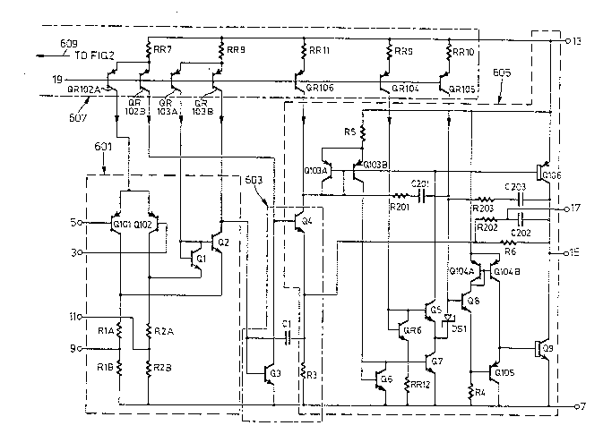
Reference will now be made to Figure l in
outlining the s-tages of an operational amplifier l according
to the preferred embodiment of the present invention. As
shown by the dashed and broken chain lines, the amplifier l
is made up of an input stage 601, gain s-tage 603, output
stage 605 and bias circuit 607. Two elements, Q4 and R3,
are cornmon to both the gain stage 603 and the output stage
605. The bias circuit 607 broken chain line is an open
ended box as a portion of the bias circuit 607, as shown by
the arrow 609 in Fig. l, continues in Fig. 2.
Referring to Fig. 2 the portion of the bias
circuit 607 appearing therein may be referred to as a
reference circuit 21.
CIRCUlT CONFIGURATION OF THE NOVEL AMPLIFIER
With reference to Fig. l, the components of the
stages 601, 603, and 605 will now be described. The
description of those components of the bias circuit 607
shown in Fig. 1 will be interwoven with the description of
the stages 601, 603, and 605 and will not be separately
described.
_ The input stage 601 has inverting and noninverting
inpu~ ^3, 5. The inputs are connected to the bases of two
PNP transistors Q101, Ql02. The transistors Q101, Ql02 are
differentially connected with the emitters of Ql01 and Q102
interconnected and connected to the collector of a current
reference transistor QR102A. The collectors of Q101 and Q102
are connected through resistors RlA and RlB, and R2A and
R2B~ respectively, to a negative supply rail 7.
~ ~3~2~3~
Offset adjusts 9, 11 are provlded between RlA and
RlB, and between R2A and R2B, respectively.
The collectors of Q101 and Q102 are also directly
connected to -the emitters of NPN transistors Ql and Q2. The
collector and base of Ql are interconnected, connected to
the base Q2, and connected to the collector of a current
reference transistor QR103A.
The collector of Q2 is connected to the collector
of a current reference transistor QR103B.
The input stage 601 is connected to the gain stage
603, the connection to the gain stage 603 and the
configuration of the gain stage 603 will now be described.
The collector of Q2 is connected to the base of an NP~
transistor Q3, and through a capacitor Cl and resistor R3 to
the negative supply rail 7.
The emitter of Q3 is connected to the negative
supply rail 7. The collector of Q3 is connected to the
collector of a current reference transistor QR102B. The
collector of Q3 is also connected to the base of an NPN
transistor Q4.
The emitter of Q4 is connected between the
capacitor Cl and the resistor R3. The collector of Q4 is
connect^ed to the collector of a current reference transistor
QR106.
The gain stage 603 and the output stage 605
overlap as mentioned previously at the components Q4 and R3.
The output stage 605 will now be described, but the
description of Q4 and R3 above will not be repeated for the
output stage 605. The collector of Q4 is also connected to
:
3~3~1
the collector and base of a PNP -transistor Q103A.
The base of Q103A is also connected -to the base of
a PNP transistor Q103B. The emitters of Q103A and Q103B are
interconnected and connected through a resistor R5 to a
positive supply rail 13. The bases of Q103A and Q103B are
further connected to the base of a PNP transistor Q106. The
emitter of Q106 is connected to the positive su2ply rail 13.
The collector of Q106 is connected to an output 15 of the
amplifier 1.
The collector of Q103B is connected to the base
and collector of an NPN transistor Q6. The emitter of Q6 is
connected to the negative supply rail 7. The collector a~nîd
base of Q6 are also connected to the base of an N~N
transistor Q7.
The emitter of Q7 is connected to the negative
supply rail 7. The collector of Q7 is connected to the
cathode of a schottky diode Sl and to the emitter of an NPN
transistor Q5.
. The base of Q5 is connected to the collector and
base of an NPN voltage reference transistor QR6. The
collector of Q5 is connected to the bases of Q103A, Q103B
and Q106.
--, 3 ~ _
The collector and base of QR6 are further
connected to the collector of a current reference transistor
~ QR104. The emitter of QR6 is connected through a reference
: resistor RR12 to the negative supply rail 7.
The anode of DSl is connected to the collector of
: a current reference transistor QR105. The anode of DSl is
also connected to the base of an NPN transistor Q8.
3~23~j~
The emitter of Q8 is connected -through a resistor
R4 to the negative supply rail 7. The emitter of Q8 is also
directly connected to the base of a PNP transis-tor Q105. The
collector of Q8 is connected to the collector and base of a
PNP transistor Q104A.
The collec-tor of Q105 is connected to the negative
supply rail 7. The emit-ter of Q105 is connected to the
collector of a PNP transistor Q104B and the base of an NPN
transistor Q9.
The bases of Q104A and Ql04B are interconnected.
The emitters of Q104A and Q104B are interconnected and
connected to the positive supply rail 13.
The collector of Q9 is connected to the output 1~
The emitter of Q9 is connected to the negative supply rail
7.
The emitter of Q4 is also connected through a
resistor R6 and through a resistor R202 and capacitor C202
to the output 15. Connected between R202 and C202 is a
frequency compensation connection 17 for the external
frequency adjustment of the output stage 605, if desirable.
; The collector of Q4 is further connected through a
reslstor R201 and capacitor C201 to the anode of DSl. The
_ c
anode of DSl is further connected through a resistor R203
and a capacitor C203 to the output 15.
The bases of QRl02A, QRl02B, QRl03A, QR103B,
QRl06, QR104, and QRl05 are interconnected and connected to
a bias bus l9.
The emitters of QRl02A, QR102B are interconnected
and connected through a reference resistor RR7 to the
positive supply rail 13. The emit-ters of QR103A, QR103B are
similarly interconnected and connected through a reference
resistor RR8 to the positive supply rail 13. The emitters of
QR106, QR104 and QR105 are connected through reference
resistors RRll, RR9, and RR10 to the positive supply 13.
The bias bus 19 is connected to a bias reference
circuit 21 as shown in Figure 2. The bias reference circuit
is part of the amplifier 1 and operates in a wholly
conventional manner.
The bias bus 19 is connected to the bases of two
PNP reference transistors QRlOlA, QRlOlB.
The emitters of Q~lOlA and QRlOlB are
interconnected and connected through a reference resistor
RRl to the positive supply rail 13.
The collector of QRlOlA is connec-ted to the
collector and base of an NPN reference transistor QRl. The
emitter of QRl is connected to the negative supply rail 7.
The collector of QRlOlB is connected to the
collector of an NPN reference transistor QR2. The bases of
QRl and QR2 are interconnected. The emitter of QR2 is
connected through a reference resistor RR2 to the negative
supply rail 7.
The collectors of QRlOlB and QR2 are further
connected to the base of an NPN reference transistor QR3.
The collector of QR3 is connected to the positive supply
rail 13. The emitter of QR3 is connected through a reference
resistor RR6 to the negative supply rail 7.
The emitter of QR3 is further directly connected
to the emitter of an NPN reference transistor QR4. The
3 ~ ~ 3 ~ gl
collector of QR4 is connected to the bias bus 19. The base
of QR4 is connected through a reference resistor R3 to the
positive supply rail 13. The base of QR4 is also connected
through reference resistors RR4 and RR5 to -the negative
supply rail 7. The base of QR4 is further directly connected
to the collector of an NPN reference transistor QR5.
The base of QR5 is connected between RR4 and RR5.
The emitter of QR5 is connected to the negative supply rail
7.
CONVENTIONAL INPUT STAGE
Reference will now be made to Figure 3 to expla-i~
the operation of a conventional PNP input stage (not o~
course shown in Fig. 1). All components of conventional
stages described hereafter will be preceded by a "C" to
differentiate them from the components used in the novel
stages.
A current source CI feeds the emitters of
differentially connected PNP transistors CQI01 and CQ102.
The collectors of CQ101 and CQ102 are connected to the
collectors of current mirror connected NPN transistors CQ103
and~CQ104.
.
~ The inputs to the input stage are an inverting
input 103 and a noninverting input 105. The output of the
stage is a current Cio representative of the differential
vol-tage at the inputs 103, 105.
In operation, the bias current CI with equal
voltages at the inputs 103 and 105 is split by the
transistors CQ101 and CQ102. Equal currents will be produced
~ ~`1`4 - ~3~23~9
in the collectors of CQ101 and CQ102. The current in the
collector of CQ101 will provide the current for the
collector of CQ103 and -the bases of CQ103 and CQ104.
As the transistors CQ103 and CQ104 are in a
current mirror configuration the current in the collectors
of CQ103 and CQ104 are similar. The current driving the
bases of CQ103 and CQ104 taken from the collector cu~rent of
CQ101 must also be removed from the collector of transistor
CQ102. This current is taken off as the bias com?onent of
the output current Cio used to bias the next stage.
In operation, when a positive going signal, as
compared to the input 103, is placed at the input 105 the
voltage across the emitter of CQ101 will decrease. The
amount of current which CQ101 will take from the current
source CI will correspondingly decrease. This decreases the
amount of current in the collector of CQ101, CQ103 and
CQ104.
At the same time, more curren-t will flow into the
emitter of CQ102 from the current source CI producing a
larger current in the collector of CQ102. The collector
current CQ102 will be greater as compared to the collector
current in CQ104. This causes an increase in the output
current Cio. Correspondingly if the input at the
non-inverting terminal 105 was decreased the current Cio
will decrease.
If a positive going voltage signal is input at the
inverting input 103 less current will flow from the
collector of CQ102 and correspondingly more current will
flow from the collector of CQ101 through the current mirrors
:
:
3~23~9
CQ103 and CQ104. This produces a decrease in the output
current Cio. Correspondingly, if the voltage is decreased at
the input 103 the output current Cio will increase.
In this configuration common mode voltages at the
inputs 103, 105 near the negative supply rail 7 will
saturate CQ101 and CQ102.
The conventional input stage may be operated with
supply voltages down to 1.0V, but it does not have negative
supply rail common mode voltage sensing capability.
Alternately CQ101 and CQ102 can be replaced by PNP
darlington connected transistors, not shown, to avoid the
above mentioned saturation. However the input stage wil~
not operate reliably on supply voltages between the positive
and negative rails 13, 7 of less than 1.5V with common mode
input voltages more positive than the negative supply rail,
since current source CI would be in saturation.
NOVEL INPUT STAGE
DIFFERENTIAL BUFFER AMPLIFIER
Reference will now be made -to Figures 1, and 4.
The ~ pUt stage 601 of the amplifier 1 has a differential
buffer amplifier section whose major components are Q101,
Q102, RlA, RlB (shown collectively as Rl in Fig. 4), R2A,
and R2B (shown collectively as R2 in Fig. ~).
DC bias current is provided by the bias circuit
607 to the emitters of Q101 and Q102. In figure 4, the
components of the bias circuit 607 current source configured
QR102A, is shown functionally as current source Il.
~:
3~ 23~9
Referring specifically -to Figure 4, the DC bias
current Il flowing into the emitter of Q101 and Q102 causes
correspondingly smaller input bias currents to be drawn into
the inverting and non-inverting lnputs 3, 5. Furthermore,
corresponding bias collector currents will flow in the
collectors of Q101 and Q102.
The collector bias currents will run through RlA
and RlB and through R2A and R2B. RlA, RlB and R2 A, R2B are
shown collectively as Rl and R2 in Figure 4.
Differential buffer amplifier section outputs 25,
27 are taken from the collectors of Q101 and Q102. This
produces an inverted differential voltage output at the
outputs 25, 27. A positive going signal at the non-inverting
input 5 produces a decrease in the current in Q101 and a
corresponding decrease in the voltage across the resistor
Rl. A corresponding negative going signal will produce an
increase in the voltage across Rl. Similarly, a positive
going signal at the inver-ting input 3 will cause a decrease
in the voltage across R2 and a negative going signal will
cause an increase in the voltage across R2.
. When Rl and R2 are similar and approximately equal
to the inverse of the small signal transconductance of Q101
and Q102, the voltage difference at the outputs 25, 27 will
be approximately the same as the voltage difference at the
inputs 5, 3.
The offset adjusts 9, 11 of Figure 1 are used in a
manner similar to those of a conventional differential
amplifier input stage, not shown, to compensate for any
internal mismatch of the components.
~ ~3:L23~9
TRANSCONDUCTANCE
Referring to Figs. 1, 4, the outpu-ts 25, 27 of the
differential buffer amplifier are connected to a
transconductance section whose major components are two NPN
transistors Q1 and Q2 biased by current sources I2 and I3.
I2 and I3 in Fig. 4 are functional representations of
current source configured QR103A and QR103B of Fig. 1.
The transconductance section takes the
differential voltage signal at the outputs 25, 27 and
conver-ts it into a single ended output current ioi. The
current ioi is representative of the inverse of the
differential signal at the outputs 25, 27.
The current sources I2, I3 produce similar bias
currents for the transistors Ql, Q2. When the voltage
signals at the outputs 25, 27 are similar Ql and Q2 act as
current mirrors similar to the conventional input stage
current mirror. This produces the output bias current
component of ioi.
When the voltage across R2 is increased, the
voltage across the emitter of Ql decreases. This causes a
greater amount of the current from the current source I2 to
flow into the base of Q2. Q2 will turn on harder taking more
of the current from I3. This causes a decrease in the output
current ioi.
Correspondingly, when the voltage across Rl is
increased Q2 tends -to shut down, turning Ql on harder and
increasing the output current ioi.
As the bias current I2 effectively feeds current
mostly to the collec-tor of Ql and much less to the bases of
~ .
123~
Q2 and Ql, the collector current of Q1, and consequently the Vbe
of Ql, remain substantially constant with respect to the
collector current and Vbe of Q2. The Vbe of Q1 acts,
substantially, as a voltage source. Aa a consequencer virtually
all of the voltage difference at the collectors of Q101 and Q102
will appear as the Vbe of Q2.
As the voltage at the inputs 5, 3 appears as the
voltage at the outputs 25, 27 and as the Vbe of Q2, the output
current of the input stage 601 is approximately the
transconductance gm2 of Q2 times the input voltage Vin at the
inputs 5, 3. Thus Q2 acts as a current gain element controlled
by the voltage at the output 25, 27~ The source of driving
current being I2.
The output voltage voi of the input stage 601 is
approximately the input resistance r ~ 3 of the transistor Q3
used in the gain stage 603 times ioi. The voltage gain of the
input s~age 601 will be approximately equal to r ~ 3 x gms.
The combined differential buffer amplifier section and
transconductance sec-tion produce a representative output current
for a given differential voltage input, as in the conventional
input stage.
The major advantage of the new input stage 601 is that
the common mode input voltage range can include voltages of
almost a Vbe below the negative supply rail 7 without
compromising low voltage signal performance; operation on l.Ov
supplies can be practical and reliable.
Additionally the transconductance section provides a
voltage level shift from outputs 25, 27 to the output of the
input stage 601. This contributes to the available
/7 13123~
~3 ~
voltage signal for driving the gain stage 603.
The novel input stage may be designed to operate
with supply voltages as low as 0.85V.
CONVENTIONAL GAIN STAGE
A conventional gain stage used in prior art
circuits (see Fig. 5) is made up of an NPN transistor CQ3
and a frequency compensation capacitor CC connected between
the base and collector of CQ3. The input current signal to
the gain stage is a current Ciig. Ciig is usually provided
by the output current of an input stage. The output current
signal is a current Ciog. The conventional gain stage is
biased by a current source CI2B.
The conventional gain stage acts as an integrator
as shown by the wave forms for Ciig and Ciog in Figures 5A
and 5B. Additionally there is a component in Ciog due to the
rising and falling edges of Ciig.
As the current Ciig reaches a rising edge of
mostly high frequency components, CQ3 is short circuited by
CC. Thus, Ciog increases by an amount corresponding to Ciig.
As Ciig flattens out and its high frequency
~content decreases, CC reverts to its role as an integrating
`~element. The increase in Ciig felt at the rising edge now
translates into greater base current for CQ3. This in turn
turns CQ3 on harder, CQ3 then takes more of the bias current
from CI2B decreaslng Ciog.
When Ciig hits a falling edge, CC again short
circuits. Ciog increases correspondingly.
; ~When Ciig flattens out, the decrease in current is
~: .
~ .
.
:
~3123~9
felt at the base of CQ3 tending to turn CQ3 off. This
increases the amoun of available current from CI2B used
for Ciog.
From Figures SA and 5B it is evident that Ciog
following the high frequency signal at Ciig has an antiphase
component with respect to Ciig. This can cause instability
when the loop is closed on the conventional gain stage.
Approximately 90 degrees of phase margin is lost using the
conventional gain stage.
NOVEL GAIN STAGE
Reference will now be made to Fig. 7 in detaili~g
the operation of the gain stage 603 of the amplifier 1 shown
in Figure 1. iig is the signal to the base of Q3, while iog
is taken from the collector of Q4. Q3 and Q4 are biased by
current sources I2B and I6. I2B and I6 are functional
representations of current source configured Q102B and Q106
from the bias circuit 607 of Fig. 1.
The operation of the gain stage 603 with respect
to a signal of the form shown in Figure 6A will now be
described. As the signal meets a rising edge, Cl short
circuits causing, as shown in Fig. 6B, a current to flow in
R3. This causes the Vbe of Q4 to decrease, decreasing the
current in Q4. R3 and Q3 act, among other things, as
current controlled voltage sources, while Q4 acts as a
voltage controlled current source. The amount of available
current from I6 for iog increases as shown in Figure 6C.
As iig flattens ou-t Cl integrates current. The
base current of Q3 increases. Correspondingly, the collector
~1123~
/ /
curren-t of Q3 increases. The base current available to Q4
from current source I2B decreases. Correspondingly, the
collector current of Q4 decreases. An increasing amount of
current from I6 is available for iog.
For a falling edge of iig, Cl short circuits
decreasing the current through R3. This decreases the
voltage at point A. The Vbe of Q4 increases, turning on Q4
harder. This increases the collector current of Q4 and
decreases the amount of available current from I6 for iog.
As iig flattens out, Cl integrates decreasing the
amount of available current at the base of Q3. This
decreases the collector current of Q3 increasing the amou-~t
of available base current for Q4. The collector current of
Q4 increases. The current available for iog from I6 is
correspondingly decreased.
It is evident from Figures 6A and 6C that the
phase difference of iog with respect to iig is positive for
all operating frequencies of the gain stage.
The 90 degree phase margin lost in the
conventional gain stage has been recove ed at relatively
high frequencies and added to the phase margin of the novel
gain stage. This contributes to the overall stability of the
amplifier 1 in closed loop operation.
This comparison between the conventional gain
stage and the novel gain stage 603 is evident in the BODE
diagrams of Figures 7 and 8.
The plots are the current gain (Fig. 7) and phase
shift (Fig. 8) of Ciogl and iog with respect to Ciig and iig
for increasing frequency. Ciogl is formed by adding a second
~ ?~ ~3123~
NPN transistor CQ4 having Ciog as the input signal to its
base and Ciogl as the collec-tor current. This allows for a
fair comparison of the conventional and novel gain stages.
The current gain for the conventional gain stage is
represented by curve Acig, while the current gain for the
novel gain stage 603 is represented by curve Aig.
The phase shif-t for the conventional gain stage is
represented by curve scig, while the phase shif. for the
novel gain stage 603 is represented by curve ~cig.
As is evident from the Bode diagrams, the gain of
the two stages is similar, each having an app-oximately -2-0
dB/decade roll off. The phase shift is initially similar
for both gain stages. As frequency increases the phase
shift ~cig becomes more positive due to the phenomenon
discussed above for the novel gain stage 603, while the
phase shift 3cig decreases at an increasing rapid rate for
the conventional gain stage due to the negative phase shift
discussed above.
The novel gain stage 603 thus produces a
relatlvely large phase margin as compared to the
conventional gain stage at relatively high frequencies. This
contributes to the overall stability of the amplifier 1.
The increase in phase margin allows the value of
the compensation capacitor Cl to be decreased, the phase
characteristics of the output stage to be poorer, or a
combination of the two.
Furthermore, the voltage seen by the capacitor Cl
is relatively low allowing Cl to be a diffused capacitor.
Diffused capacitors may be made on a semiconductor chip,
~ ~3~2~9
decreasing the overall size of the amplifier 1. This contrasts
with the higher voltage seen by capacitor CC in the conventional
gain stage, which often requires CC to be an external component.
The voltage gain of the gain stage 603 may be
approximated using the circuit of Fig. 9. When combined with the
output stage 605 of ~he amplifier 1 of Figure 1 there appears a
feedback loop produced by the gain of the output stage and R6.
The gain of the output stage 605 has been shown functionally by
an inverting amplifier Al and R6 in Figure 9. This feedback
network can decrease the voltage gain of Q4, but is capable of
dramatically increasing the input resistance of Q4 as seen from
the base of Q4.
As the voltage gain of Q3 is given by the
transconductance of Q3 ~m3 times the resistance of the load seen
by the collector of Q3, and this resistance is large as explained
above, the gain of Q3 will be correspondingly large.
The voltage gain of Q4 is relatively small due to the
~ feedback network previously described. Thus the overall voltage
.~ .
gain of ~he novel gain stage may be approximated by multiplying
the gm3 of Q3 by the input resistance of Q4 in parallel with an
output resistance ro of current source I2B.
CONVENTIONAL OUTPUT STAGE
Reference will now be made to figure 10 in describing
the operation of a conventional output stage. An input current
to the conventional output stage is Ciio. Ciio is normally
derived from Ciog of the conventional gain stage.
' ,;
o~ ~ 3~2~
Ciio is provided to the base of a PNP transistor
CQ200. The collecto of CQ200 is connected to the negative
supply rail 7. The emitter of CQ200 is connected -to the base
of a PNP transistor CQ201, and through series connected
diodes CDl and CD2 to -the base of an NPN transistor CQ202
and to bias current source CIB.
The collectors of CQ201 and CQ202 are respectively
connected to the negative supply rail 7 and the positive
supply rail 13. The emitters of CQ201 and CQ202 are
interconnected and connected to the output 100 of the output
stage. An output current Cioo flows from 100.
In operation current sourceCIB biases the output
stage to produce a current ICQ flowing in each of the
emitters of CQ201 and CQ202 with only a bias signal as Ciio
and zero output current Cioo.
ICQ is determined as follows; CDl and CD2 are
diodes, usually in close physical proximity to output
transistors CQ201 and CQ202. In manufacture, CDl and CD2
are also usually fabricated such that their electrical
characteristics closely match and track those of CQ201 and
CQ202.
- Applying the above conditions, and Cioo zero, it
' ~2~
is evident that if CDl tracks electrically with CQ201, and
CD2 tracks electrically with Q202, then the voltage at the
mid-point between CD1 and CD2 will ideally equal the voltage
at the output 100. The output may thus conceptually be
shorted to the mid-point between the CDl and CD2, not shown,
without altering the equilibxium of the conventional output
stage. It is now clear that CD2, CQ202 and CDl, CQ201 each
`` ~312~
represent current mirrors, eonnected serially, and having
curren-t source CIB as a common reference. Thus, ICQ is
determined to be a constant faetor times the referenee
eurrent, CIB. The constant factor is determined by the
physical area ratios of CQ202 to CD2 and CQ201 to CDl, which
ideally are the same for each diode-transistor pair.
To approximate the operating conditions of the
conventional output stage, the output stage must be operated
with a load, shown by RL in Figure 10. When Ciio is
decreased, less current flows in CQ200. Less current will
flow in CDl, CD2 and CQ201. More of CIB must flow into t~e
base of CQ202 turning CQ202 on harder. CQ201 aceepts less
eurrent from CQ202 or else the total eurrent in CQ200 would
be the same. As CQ200 is aeeepting less eurrent, some
current from the emitter of CQ202 must be flowing into RL.
As eurrent is flowing into RL, Cvoo must be positive.
Assuming CIB is a current source connected bipolar
junetion transistor, the maximum level of Cvoo will be
limited by the Vbe of CQ202 and the saturation voltage
Veesat of IB.
Correspondingly, if Cioo is inereased more eurrent
wilI_flow from CDl, CD2 and CQ202 into CQ200. This will
deerease the available eurrent in CQ202 tending to shut it
off. As the total amount of eurrent in CQ200 must have
inereased CQ201 must have more base eurrent and henee
emltter eurrent than CQ202. The extra eurrent must be
supplied from the load RL. As eurrent is following into the
output 100, the output voltage must be negative.
The maximum negative output voltage will be
'~
- 13~23~
limited to the Vbe of CQ201 plus the Vcesat of CQ200 above
the negative supply rail 7.
The conventional output stage is typically
correctly based only at voltages above 1.5V. Additionally
for voltages as low as 1.5V the stage has zero output swing
capability and is usually only useful for practical
operation at higher voltages.
NOVEL OUTPVT STAGE
Since the output stage 605 of Eig. 1 includes the
improvements of an alternate output stage configuration 609,
shown in Fig. 11, plus additional refinements, for
simplicity the alternate configuration 609 will be explained
first. Where the components are the same as those described
in Figure 1, similar reference identification has been used
and the description will not be repeated.
In the novel output stage of Figure 11 the voltage
swing limits are decreased by using common emitter
transistors Q106 and darlington pair QD, Q9. The output
voltage is limited by only the saturation voltages of Q106
and QD, Q9. The refinements section will explain a
conf~guration for a low voltage darlington as has been
employed in Figure 1.
The novel output stage 609 although conceptually
simple is difficult to bias.
Firstly, the circuit may be thought of having R5
as a short circuit. With no current at the output 15, the
quiescent current Iq is determined by current source I REF.
As the darlington pair QD, Q9 require very little current
3~23~
input, current mirror connected Q6, Q7 produce approximately
IREF in the emitters of current mirror connected Q103A,
Q103B. As the Vbe's of Q103A, Q103B and Q106 are similar, Iq
will be approximately equal to IREF.
The current needed to bias the output stage may be
decreased by increasing the area factor of Q106 as compared
to Q103A, and Q103B by a factor N. Iq will then be
approximately NxIREF.
To effectively further increase the area ratio of
Q106, R5 has been added. As the base-emitter junction of
Q106 may be thought of as a forward biased PN junction the
diode law Iq = Io (e BE106 / V -1 ), where Io and VT are
transistor parameters, applies. VBE106 may be broken down
into ~V plus VBE103B, where AV is the voltage across R5.
I (e VBE103 + ~V VT -1). As shown above when
~V = O, Iq - NIREF. Therefore, NIREF = Io (e / T_l)
and VBE103 / VT = 1 ~ NIREF/I- Substituting for
e leaves Iq - NIREF e ~ V/VT As current may only
flow into the emitters of Q103 A, B ~ V is always positive.
R5 has increased the effective area of Q106 by a further
factor of e ~V/VT
As R5 carries the current of approximately 2xIREF,
~V is approximately equal to 2xIREFxR5.
Therefore, the quiescent current Iq can be
accurately and repeatably set by the proper selection of
IREF and R5.
In operation, if the base current of Q4 is
increased a current greater than IREF will flow into Q6. Q7
will draw away all of IREF, saturating Q7 and shutting off
C,~
312~
QD and Q9. Meanwhile, more current will be drawn from the
base of Q106 and from current mirror Q103A, Q103B. This
increases ~V and increases -the proportlon of current
flowing in Q106. This current will flow to the output 15.
If the base current of Q4 is decreased from IREF
less current will be drawn from the base of Q106, tending to
shut it off. Less current will flow in the current mirrors,
Q103A, Q103B, Q6, Q7. A greater amount of current from
current source IREF will be available to drive the
darlington pair QD, Q9. Current will be drawn from the
output 15 into the collectors of QD, Q9 bringing down the
voltage at the output 15.
The novel output stage 609 can be correctly biased
at voltages as low as 0.9V. Q106 will have substantial
voltage swing capability at this point.
REFINED NOVEL OUTPUT STAGE
As the current gain of the Darlington pair QD, Q9
is very large there is no need to enhance it as for Q106.
To decrease the negative voltage limit of the
Darli~gton pair, the refinements of Figu e 1, as also shown
in FP~uEe 12, have been added to the output stage 609.
Again, the same components o Figures 1, 11, 12 will be
given the same reference identification. IREF of Figure 12
is a functional representation of current source configured
QR105 of Figure 1. Vclamp is a functional representation of
diode connected QR6, RR12, and current source configured
QR104 of Figure 1. I6 is a functional representation of
current source configured QR106.
2 ~
G17
QD has been replaced by Q104A, Q104B, Q8, Q105 and R4.
~hese components together perform a similar function to QD. As
the base current of Q8 increases, the collector and emitter
current increase correspondingly. The collector current is
mirrored and appears as the collector current of Q104B.
Meanwhile the voltage across R4 increases with the increased
emitter current of Q8. R4 acts as a current controlled voltage
source. This decreases the VBE of Q105 tending to shut it off.
Q105 acts as a voltage controlled current gain element. The
increased current in the collector of Q104B plus the current
formerly in Q105 flows into Q9. As with QD, the base current of
Q8 is amplified and fed into the base of Q9.
The advantage of these new components is that Q9 may
be taken into saturation decreasing the negative output voltage
limit to the saturation voltage VCESat of Q9.
When the current in the base of Q4 increases from the
current which produces Iq, the current in Q6 will be greater than
IREF. As the only current available to Q7 is IREF, Q7 will
saturate.
When the current at the base of Q4 decreases, Q7 must
first come out of saturation before producing substantial current
for the darlington pair or the refined darlington. Furthermore,
the voltage at point E will be pulled down when Q7 saturates.
Any stray capacitance at E will have to be charged as Q7 comes
out of saturation. The current source charging this capacitance
is IREF. IREF is relatively smaIl. The process of bringing Q7
out of saturation can cause dynamic crossover distortion at the
~3~2~5~
output 15.
To decrease the possibility of dynamic crossovPr
distortion Q7 is clamped at a level just into saturation by Q5
and a voltage clamp, Vclamp.
From Figure 1, the voltage of Vclamp is approximately
the VBE of QR6 plus the voltage across RR12. The voltage across
RR12 is determined by the current from QR104 and the value of
RR12.
As the voltage of the clamp is equal to ~he VBE of Q5
plus the VCE of Q7, the voltage of Vclamp should be set
approximately a VBE plus VCESat of Q7. Since Vclamp is equal to
a VBE plus the voltage across RR12~ VRR12, VRR12 should be set
at VCESat.
When the output current at the output 15 is zero,
approximately all of IREF flows into Q7. The VCE of Q7 will be
relatively large~ The VBE of Q5 will be relatively small, Q5
conducting a negligible amount of current.
As Q7 draws more current than IREF Q5 will begin to
conduct more. The VBE of Q5 will increase and the VCE of Q7 will
decrease. Q7 will go into soft saturation, its voltage clamped
at VCESat. In this way Q7 is prevented from entering into the
hard saturation region.
The current in the collector of Q5 will be drawn from
the base of Q106 increasing the available current to drive Q106.
Thus Q5 acts as a current switch drawing current into current
mirror Q6, Q7 when Q106 is being driven.
As Q5 effectively replaces the current removed
. ~
., .
:1312 3 ~
from the base of Ql06 by Q103A, virtually all of the drive
curren-t suplied by Q4 is available as base current for Q106
when Q5 is in conduction. R5 limits the currents in Q103A
and Q103B and correspondingly in Q6 and Q7.
The Schottky diode dsl decreases the increase in
voltage at Q7 necessary to turn on Q8 and Q9. As dsl is
conducting when Q7 comes out of saturation, the voltage at
the base of Q8 is approximately Vcesat plus Vdsl. A
relatively small inc~ease in the VCE of Q7 will cause Q8 to
turn on. This further decreases the dynamic crossover
distortion at the output.
The novel output stage 605 can be correctly biased
at voltages as low as 0.85V with substantial output swing
capability at this point.
While the present invention has been disclosed in
connection with the preferred embodiment therof, it should
be understood that there may be other emhodiments which fall
within the spirit and scope of the invention as defined by
the following claims.
:~:
~ .
.