Note: Descriptions are shown in the official language in which they were submitted.
~2~2
FRAME SYNC~IRO~I~ATlON IN ~ N~UTORl~
OF 'rIME MULTIPL~XED OPTICAL SPA(~E ~WITCH~S
This invention relates to a network of time mult;plexed optical spaee
s-vitches and more partieularly to synchronizing frames of data in such a
5 network.
Background OI the Invention
Optical transmission systems are increasingly used in
telecommunieation networks. They provide a relatively low eost, wideband
transmission medium which supports many communication patlls over eaeh
10 optieal fiber. Voiee, data and video signals are transmitted through the
fibers as optieal digital signals to minimize noise and distortion over long
distanees.
Beeause of the inereased use of lightwave technology in
transmission systems, there is interest also in using optical technology in
15 switching systems for intereonnecting a network of optical transmission
systems. One advantage in using optical switching is the potential for
eliminating the electrical-to-optieal and optieal-to-eleetrieal eonversions
whieh are now required between the optical transmission systems and the
existing electrical switching systems.
Frequency and frame synchronization are very important factors
in an optical switching network. Very high bit rate bit streams from a
variety of transmission systems must be coordinated for eoineidental
switehing through the optieal switehes. Eaeh sequential stream of
information bits is grouped into a framed format. Within eaeh frame, the
25 bits are grouped aeeording to-their destina-tion. Sueh groups of bits are
ealled data segments. Following eaeh data segment is a gap referred to as a
guard band, or switeh reeonfiguration time. The purpose of the guard band
is to provide time for reeonfiguring the switeh while allowing for time
misalignment ot frames arriving from cli-fferent transmission system inputs
30 to the switeh. This type of multiplexing is known as bloek multiplexing.
~ Iaving grouped the infor-mation bits within eaeh frame into data
segments aeeording to destination, it is possible to route the bits to their
destination by properly eonfiguring elosed erosspoints in the optical switeh
during the guard bands. Switch reconfiguration must occur while the guard
:~3~26~
bands concur for all data streams arriving at the optical switch. C)therwise
the switch reconfiguration occurs while one or more data segments are
arriving at the switch and some data will be lost.
~n optical switch may be of a variety of types; however, an
5 optical space s~,vitch, based on titanium-diffused lithium niobate (Ti: Li Nb
O3) directional couplers, is a reasonable option for early opt;cal switching
systems. The directional couplers can be arranged iIl a crossbar format. In
non-blocking optical switches, the state of each directional coupler is
subjeet to ehange periodically several times per frame of information. The
10 states of the direetional eouplers are ehanged so that every input ean be
eonneeted to every output at least onee during every frame.
There are problems assoeiated with the design of a
synehronization arrangement for an optieal switeh. First of all it is essen-tialthat the frames of data arriving at every optical switeh are all synehronized
15 with each other and with the switch itself. They must be synchronized in
both frequency and in phase. ~ny synchronization arrangement can use no
more than a reasonable amount of equipment at a reasonable cost.
Seeondly it is important to design the synehronization arrangement for
minimal operating eost. Beeause there are guard bands between the data
20 segments in the signal stream, there is a potential for inefficient operationsince operating efficiency is defined as the quantity frame duration time less
total overhead time in one frame divided by total frame duration time.
Typieal designs for optieal switehing networks cover large
geographie areas and inelude optieal transmission systems that are several
25 hundred to several thousand miles long. The intereonneeting eables which
inelude the optieal transmission media are subjected to wide differenees of
environmental eonditions and temperatures. As a result, the total duration
of guard bands per frame tends to be very long in relation to the length of
the frames. Sinee effieieney of operating the network is determined by
30 dividing the quantity frame duration time less the total duration of the
guard bands and other overhead time per frame by the frame duration time,
long guard bancls tend to make the network ineffieient and relatively more
expensive to operate. Sueh ineffieieney presents a problem for designers of
optieal switehing networks.
13:~2~
~ummary o l~ the Inven tion
This problem and others are solved by an optical switching
network including a master optical switch that is interconnected with
remote slave equipments ïor switching block-multiplexed messages among
5 the remote equipments. The master optical swi-tch responds to a frequency
reference clock and steps periodically through a sequence of states for
establishing various routes, i.e., the switch connections are reconfigured
periodically for establishing different connections between its inputs and
outputs, among the remote equipments for appropriately routing the
10 messages to correct destinations. The frequency reference clock is
distributed from a common source to the master optical switch and to the
remote slave equipments. During one of sueh states per frame, eaeh remote
slave equipment transmits a distinct signature signal. All of the slave
equipments are connected through the master optical switch to return to
15 themselves their own signals transmitted during that -time slo-t. Each
remote slave equipment compares the returned signal with the originally
transmitted signature signal to determine how mueh round trip delay has
varied from a nominal value and then adjusts the phase of a control clock
signal to counteract the variation of the delay. Thus the -time of operation
20 of the remote slave equipment is adjusted and synchronized with the master
optical switch so that messages transmitted from the remote equipment
arrive at the master optical switch at the eorrect time with respect to the
periodic reconfigurations of the master op-tical switch. Sinee the messages
from the various remote slave equipments are synchronized to arrive at the
25 master optieal at the eorreet reeonfiguration times, the recluirecl guard
bands and total overhead time per frame are redueecl -to a very short time.
Efficieney of the network is thereby inereased substantially.
In a network of optieal switehes for routing bloek-multiplexecl
messages, one optieal switeh is designated a mas-ter and the other optieal
30 switehes are slaves. A slave switeh ean in turn aet as a mas-ter of other
lower-level slave switches, so that control of the network is exercised in a
hierarehieal fashion. All of the switehes are reeonfigured periodieally for
routing different inputs to outputs. The phase of the eontrol elock signal
for each slave optieal switeh is adjustecd so that its transmitted data
35 messages arrive at the master optieal switeh at the eorreet times with
respeet to the periodie reeonfigurations of the master optieal switeh.
~ 3 ~ C~J
Variable lurnped optical delay u nits are placed in the fibers which are used for
transmitting From the master optical switch to the slave optical switches. These lumped
optical delay units are controlled so that optical signal messages, transmitted from the
master optical switch, arrive at each of the slave optical switches at the correct times with
S respect to the periodic reconfigurations of the slave optical switches. As a result, the
network of optical switches is synchronized so that the required guard bands and total
overhead time per frame are reduced and efficiency increased accordingly.
In accordance with one aspect of the invention there is provided a method
for synchronizing a remote slave equipment with a master photonic switch comprising the
steps of: producing at the remote slave equipment a control clock signal from a frequency
reference clock; repeatedly transmitting from the remote slave equipment to the master
photonic switch block multiplexed messages including a signature-sequence of bits du}ing a
predetermined time slot of every frame generated in response to the control clock signal;
feeding back at least a portion of the signature-sequence of bits from the master photonic
switch to the remote slave equipment during the predetermined time slot of every frame;
the remote slave equipment comparing the fed back port;on of the signature-sequence of
bits with the signature-sequence of bits for determining a phase difference therebetween;
and adjusting, in response to the phase difference, the phase of the control clock signal
with respect to the frequency reference clock.
In accordance with another aspect of the invention there is provided an
optical communication network having an optical switch controlled by a frequencyreference clock for routing block multiplexed optical signals rom plural inputs to plural
outputs, an end terminal controlled by a control clock signal derived from the frequency
reference clock, first and second optical fibers interconnecting the end terminal with an
input and an output of the optical switch, the network comprising: means for generating a
signature signal in the end terminal and transmitting the signature signal through the first
optical fiber to the input of the optical switch; the optical switch configured, while the
signature signal is being transmitted, for routing the signature signal from the first optical
fiber and the input through a crosspoint in the optical switch to the output and the second
fiber for return to the end terminal; means within the end terminal for comparing the
returned signature signal with the transmitted signature signal to produce a phase
difference signal; and means responsive to the phase difference signal for adjusting the
phase of the control clock signal with respect to the frequency reference clock.,~
~a
Brieî Description oE th~ Dra~Yin~~
The inventio!l will be better understood by reading the following detailed
description with ret`erence to the drawing wherein
FIG. 1 is an illustrative timing diagram oE a sequence oE bits in a Erame
S Eormat including N+1 time slots per Erame;
FIG. 2 is a schematic diagram oE a Eour-by-four switch interconnected with
four remote terminals;
FIG. 3 is a timing cliagram for switch reconfigurations oE the four-by-Eour
switch oE FIG. 2;
l() FIG. 4 is a hlock diagram oE a remote slave equipment interconnected with
the four-by-four switch ot FIG. 2; and
FIG. 5 is a block diagram oE a network of optical switches and
interconnecting optical fiber lines.
Detailed Description
An optical space switch in a crossbar Eormat receives inputs of time-
multiplexed photonic signals. The input photonic signals are in a block-multiplexed
Eormat. In a block-multiplexecl Eormat, bits are grouped in blocks according to their
destinations. The optical, or photonic, switch uses such a block-multiplexed format
because the selected routes through the switch must be reconEigured for every change of
20 destination. Thus the switch is reconEigured periodically Eor rearranging the routing oE
blocks oE data arriving at the switch. Switch recon~igurations at the block rate are much
less Erequent than reconfig-lrations at the bit rate and can be accomplished with present
technology.
ReEerring now to FIG. 1, there is shown an example of a sequence of
25 blocks of sequential data on a time line. The blocks are arranged in a frame
wherein a first block n is Eollowed by a block n + 1, and so on until a block
n + N, the last block oE the Erame. Then the
r~
, 2 ~ ~ C,~
design3tions o~ the blocl~s repeat in a subsequent frame, not shown.
Each block of data is included in a time slot. The time slot is
long enough to include both a block of data and a guard band. The guard
band is included in each time slot to compensate for any misalignment of
5 the frames of data which are transmitted from different sources. Frames of
data received by ~ switch fronl different end terminals generally are not
fully aligned, i.e., the first bit of data in the frame from one end terminal
does not arrive at the switch at the same time as the rlrst bit of data in the
frames of all other end terminals.
A frame synchronization problem is caused by those differences
in the phases of signals arriving at the switch from the different sources.
These differences in phase are a result of the variations in the time of
transmission of photonic signals from end terminals, the ambient changes
along cable routes and the changes in transmitter laser frequencies. (~uard
15 bands in the block format must be long enough to accommodate the
maximum expected phase variations from all of those factors. As previously
mentioned, the instants of switch reconfigurations must occur within the
guard band of every input bit stream or else data is lost. ~Ieretofore to
accommodate the largest expected phase variations, the guard bands have
20 been so long that they occupy something in the order of one thousand bits
per time slot. That is excessive operating overhead for any network of
commercial significance. Operating such a system is just too inefficient and
costly.
Referring now to FIG. 2, there is shown a block diagram of an
25 optical space switch 30, arranged in the form of a crossbar matrix switch,
which is interconnected with four end terminals 32, 33, 3~L and 35.
Crosspoints in the matrix are based upon known photonic directional
couplers, such as the previously mentioned titanium-diffused lithium
niobate directional couplers.
During operation of the optical switch 30, control circuitry (not
shown) periodically reconfigures the paths thro-ugh the swi-tch in response -to
control signals with reference to a mas-ter frequency clock 31. Each time the
paths through the swi-tch 30 are reconfigured, each end terminal 32, 33, 34
and 35 is connected through the switch to one of the end terminals. Thus
35 signals arriving at any one input of the switch 30 can be routed to a
different output and end terminal every time the switch is reconfigured.
~ 3 ~ ~ ~3 ~
Referring IIOW to FI(~. 3, there is shown a diagram presenting
variations of time slot times of arrival receivecl at the switch 30 of FI~. 2
from the end terminals 32,33,34 and 35. Each line across the diagram
represents a sequence of data originating from one terminal. Four time slots
5 are shown from lert to right~ They are represented by vertical divisions,
which are numbered 1 through ~ across the bottom of the figure~
Crosspoint connections, which exist during each time slot, are indicated by
dots on the small matrix located direc-tly below the associated time slot.
Signals from any given end terminal are transferred through the switch 30
10 to a specific output according to the switch path configuration represented
in the matrix for each time slot.
In the switch configuration of the leftmost time slot, the
crosspoints are closed along the diagonal from the upper left to the lower
right. At such a time, the signals, transmitted in the FI(~. 2 by the end
terminal 32 through a fiber 36 to the switch 30, are routed through a closed
crosspoint 3g, are carried through another fiber 39, and are fed back to the
receiving port of the end terminal 32. Likewise concurrent transmissions
from the end terminals 33,34 and 3S are routed respectively through closed
crosspoints 'l1, ~3 and '15 and are fed back to their own receiving ports.
This just-described switch configuration generally is not used in
the ordinary sequence of operations by the switch 30 because each terminal
has its output fed back to its own input port. Operation in this
configuration is referred to hereinafter as feedback operation. By
transmitting special signature signals from each end terminal 3~,33,34, and
25 35 during such switch configuration ancl analyzing the returned signature
signals within receiving circuitry in each end terminal, the round trip delay
(from the end terminal through the switch 30 and back) can be determined
for each end terminal. Any variation of such delay also can be determined
so that compensating changes of phase can be made in local clock signals
30 used for controlling each of the end terminals.
In FIC~. 3, the reconfiguration patterns shown during the time
slots 2,3 and 'I allow for full inter-connectivity among all of the end
terminals. Depending upon traffic needs, one or more of the switch
configurations can be repeated during every frame of bits.
~2~C~
- ~ -
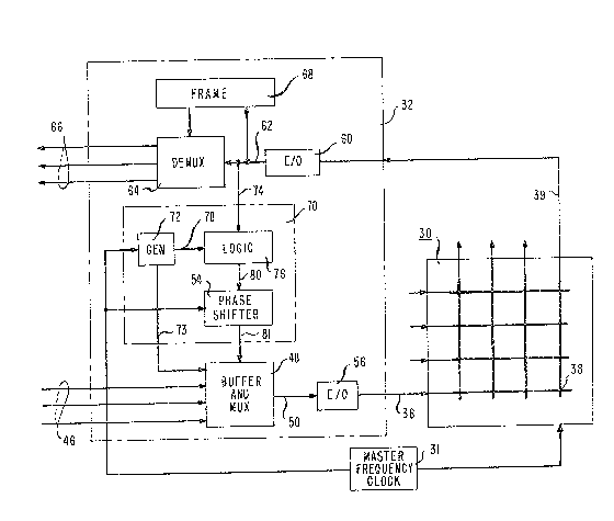
Referring now to ~IG. ~1, the end term;nal 32 is shown as a more
detailed block diagram interconnected by way o:f the optical fibers 36 and
39 with the optical space switch 30. In the end -terminal 32, a group of
input leads ~16 apply electrieal bit streams to the inputs of a buffer and
5 multiple~cer 48. Those input electrical bit streams together with a b;t
stream on lead 73 are combined into a single block multiplexed electrical bit
stream on a lead 50 under timing control from signals applied from a phase
shifter circuit 5~ The bit stream on the lead 50 is applied to an electrical-
to-optieal converter 56 and is converted into a representative optical bit
10 stream on the optical fiber 36.
In the switch 30, the crosspoints are configured during the first
time-slot so that the crosspoint 38 is closed to route the bit stream from the
optical fiber 36 to the optical fiber 39 and on to the receiving port of the
end terminal 32. There the optical bit stream is converted by an optical-
lS to-electrical converter 6Q into an electrical bit stream on a lead 62. That
electrical bit stream is applied to a demultiplexer 6'1 which splits the bit
stream into blocks which are directed to appropriate destinations located
along lines 66.
~ framing and control circuit 68 provides a source of timing
20 signals, derived from the received bit stream, i'or controlling the timing of the demultiplexer 6~.
~ control circuit 70 adjusts the timing of the master clock
signals from the master frequency clock 31 in dependence upon the duration
of round trip delay as determinecl by the process of sending the special
25 optical signature signal bit stream through the fiber 36, the switch 30 and
the fiber 39 back to the terminal 32, as -the returned signature signal. ~
specific signature signal representing the end terminal 32 is generated by a
generator circuit 72 and is applied by way of the leacl 73 to the input of the
buffer and multiplexer a~8. The signature signal bit stream includes a prefix
30 string of "1's" followed by a distinctive bit pattern identifying the end
terminal 32 and a suffix string of "1's". When that signature bit stream is
fed back to the input port of the terminal 32, the electrical bit stream is
carried through a lead 7~ to a logic circuit 76. In the logic circuit 76, the
returned bit stream is compared with a replica of the -transmitted signature
35 signal bit stream on a lead 78 for determining how much the returned bit
stream varies in phase from its appropriate timing. The logic circuit 76
~ 3 ~
looks at a sarmple o~ the returned bit stream during the time that the
signature signal bit stream is expected to return. Logic circuit 76
determines whetller or not the signature signal ior the terminal 32 is
returned during the appropriate time slot. It might be shiftecl either ahead
5 of or behind the appropriate time. If the signature signal for the terminal
32 is not returned during the appropriate time slot, the phase of the local
control clock produced on the lead 81 by the phase shifter circuit 54 is
adjusted with respect to the master clock frequency reference from the
master frequency clock 31. This process is repeated until the signature
10 signal bit stream for the terminal 32 is returned to the end terminal 32
during the appropriate time slot.
When the correct signature signal bi-t stream is received during
the appropriate time slot, the logic circuit 76 looks ror all of the prefix and
suffix "1" bits. If all of those bits are returned during the appropriate time
15 slot, no further adjustment is made to the phase of the local control clock
produced by the phase shifter circuit 5~. The slave end terminal 32 thus is
synchronized with the master optical switch 30. If less than all of the prefix
bits are returned, the phase of the local control clock on the lead 81 is
delayed under control of a signal on the lead 80. If less than all of the suffix20 bits are returned, the phase of the local control clock on the lead 81 is
advanced by the signal on the leacl 80. In eîther case, the phase of the local
control clock is adjusted to counteract the variation in delay which has
occurred along the optical paths 36 and 39 and at other places between the
end terminal 32 and the optical switch 30.
Logic circuit 76 produces on the lead 80 a signal representing the
magnitude and the polarity oi adjustment that the phase shif-ter circuit 5
must make in the local control clock signals derived from the master
frequency clock 31. The circuit 76 alternately searches for the signature
signal and adjusts the phase of the local control clock signal relative to the
30 frequency reference, or master, clock 3~ as applied through the signature
signal generator 72 and the lead 78. Changing the phase of the local control
clock signal on the lead 81 also changes the time at which the signature
signal bit stream arrives at the optical switch 30. After appropriate
adjustment of the phase of the local control clock on the lead 81, the
35 signature signal arrives at the optical switch 30 in synchronism with the
master frequency clock signal controlling the optical switch 30. The optical
~ 3 ~ f''~3~
switch will be recon~igured during the guarcl bancl prece~ing the designated
time slot for arrival of the signature signal. All of the signature signal,
including prefix and sufrlx bits, is routed to the optical fiber 39 which
carries the entire signature signal back to the receiving port of the end
5 terminal 32. Since the entire signature signal is received, the frame of data
transmitted from end terminal 32is locked in synchronism with the master
frequency clock controlling the switch 30.
Once the end terminals are locked with the master optical switch
30, each can detect subsequent loss of one or more bits from the prefix or
10 the suffix of its signature signal and make minor adjustments to the phase
of its local control clock signals for maintaining synchronization.
Adjustment of the phase can occur during every frame of data. Such
constant adjustment maintains synchronization with very close tolerance.
The required guard bands therefore are shortened with respect to the
15 lengthy duration which was required heretofore. Extra time required for
transmitting the signature signals once during every frame is offset by a
much more substantial reduction in the guard bands of every frame. Total
o~erllead therefore is recLuced substantially, and the network operates much
more efficiently. Each of the end terminals 32,33,34 and 35 of FIG. 2 has
20 an exclusive signature signal bit s-tream with prefix and suffix bits. These
signature signals can be distinguished from each other and from cllstomer
data so that each end terminal can correctly identify its own signature
signal and round trip delay. Thlls each end terminal is capable of
synchronizing transmitted frames of bits with the reconfiguration times of
25 the optical switch 30. Once all of the end terminals are synchronized with
the optical switch 30, all data in the network is routed and periodically
rerouted through the op-tical switch 30 without losing or dropping any bits.
Referring now to FIG. 5, there is shown a network of optical, or
photonic, space switches 100, 110 and 120. The switches are shown as 4xa~
matrices, as in FIG. 2. All of the optical space switches 100, 110 and 120 of
FIG. 5 can be interconnected with various end terminals, in accordance with
the arrangement of FIG. 2. Also the optical switches 100, 110 and 120 are
reconfigured periodically (every time slot) to route incoming bit streams of
data to the various outputs. The optical switches provide full connec-tivity
35 between inpu-ts and outputs during every frame of data. This network
presen-ts one synchronization problem, which is solved by a process similar
2~
- 10-
to the one just described with respect to FIGS. 2, 3, and ~l, and other
synchronization problems that are solved by other processes.
With respect to the one similar solution, -the optical switch 100
acts as a master to both of the other optical switches 110 and 120. Master
frequency clock 31 applies reference frequency clock signals to all three
optical switch locations so that they operate in reference to a single
reference frequency clock source. Once per frame of bits, a distinctive
signature signal is generated by each of the circuits 155 and 125. Those
electrical signature signals are converted -to optical signature signals by
10 electrical-to-optical converters 139 and 1~0, respectively. The optical
signature signals are applied to the respective slave optical space switches
110 and 120 for routing through optical fibers 135 and 138 to the master
optical space switch 100. By the configuration of the master optical switch
100, the optical signals are routed through the master optical switch and
15 back to their source locations by way of optical fibers 111 and 121. These
optical signals, fed back to the circuitries 130 and 131, are converted from
optical signals to electrical signals by optical-to-electrical converters 13~ and
12~1. By way of leads 125 and 127 the returned electrical signals are applied
to the circuits 155 and 12S for comparison with the distinctive signature
20 signals which were sent to the master optical switch 100. ~ny phase
adjustment, required as a result of the comparison, is imparted to the
control clock signals on the leads 15~ and 128. These phase adjustments are
made with reference to the reference frequency clock signal from the master
frequency clock 31. In this operation, each of the circuitries 130 and 131
2S scans for the appropriate signature signal and adjusts the phase of its localcontrol clock signal, as required, so that all customer data, transmitted from
the slave optical space switches 110 and 120, arrive at the mas-ter optical
switch 100 at the appropriate time with respect to every reconfiguration of
the master optical switch 100.
Another synchronization problem is to assure that all customer
data, sent from the master optical switch 100 to either of the slave optical
space switches 110 or 120, arrive at the destination slave switch at the
appropriate time for its reconfigurations. This problem is solved by
adjusting delay in the paths through the fibers 111 and 121 carrying data
from the master optical switch 100 to the slave optical switches 110 and 120,
respectively.
.~312~3'~
Frames of optical data signals from the master optieal switch 100
are transmitted through the optical fiber 121, a variable optical delay device
122, and a fiber 123 to the slave optical space switch 120. The frames of
optical data signals from the fiber 121 also are applied to an optical-to-
S electrical converter unit 124. This converter unit 12~ together with asignature signal generator and clock phase control circuit 125 are similar to
part of the arrangement of FIC~ . A delay adjustment circuit 126,
responsive to the frames of received electrical signals by way of a lead 127,
determines the starting times of the received frames of bits. The delay
10 adjustment circuit 126 compares the timing of the received frames of bits
with the framing of the local control clock signals on lead 128 and produces
a signal on the lead 129 to adjust the delay of the variable optical delay
device 122 so that frame times of optieal signals arriving on the fiber 121, as
applied through the fiber 123 to the switeh 120, are appropriate for the
15 reeonfiguration timing of the slave optieal space switch 120.
Slave optical switch 110 of FIG. 5 is synchroni~ed with the
master optieal switch 100 in a manner similar to that just described with
respect to the slave optical switch 120.
An additional synchroni~ation problem is to assure that data,
20 originating at either of the slave optical space switehes 110 and 120 arrives at the other slave optical switch at a time appropriate for the
reconfiguration timing of the receiving slave optical switch. Frames of
optical data signals from the slave optical switch 110 are transmitted
through an optieal fiber 141 and are applied through a variable optical delay
25 device 1~2 and a fiber 143 to the slave optieal switeh 120. Frames of optiealdata signals from the fiber 1~1 also are applied to an optieal-to-eleetrieal
eonverter unit 1~14. A delay adjustment eireuit 146, responsive to the
eleetrieal data signals from the converter unit 14~, determines the starting
times of frames. Frame timing is eompared with the local eontrol clock
30 signal on the lead 12~. Delay adjustment circuit 146 produces a control
signal on the lead 1~1~ to adjust -the delay of the variable optical delay unit
1~2 so that the frame times of optical signals arriving on the fiber 1a~1, as
applied through the fiber 143 to the switch 120, are appropriate for the
reconfiguration timing of the slave optical switch 120.
L 2 ~
,A variable optical delay device 1S2 is adjusted to synchrollize
optical data signals arriving at the slave optical switch 110 by way of the
optical ~iber 15L so that frames of those signals are timed appropriately with
the reconfiguration timing of the slave optical switch 110. This function is
5 accomplished in a manner similar to the process just described with respect
to data sent from the slave optical switch 110 to the slave optical switch
120.
The foregoing describes an arrangement of an optical switching
net~vork that is synchronized throughout in frequency and in phase.
10 Frequency synch~onization is accomplished by distributing the master
reference frequency clock to control all nocdes in the network. Phase
synchronization is accomplished in part by adjusting the phases of all local
clock control signals with respect to variations in round trip delay
experienced by the signature signals. Additional phase synchronization is
15 accomplished by adjusting the delay in optical paths between nodes in
response to the detected difference between the frame times of received
frames and the frame times of the local clock control signal.
All of such synchronization substantially recluces the variations
of frame timing among the different sources of data being received at each
20 node. As a result the required duration of guard bancls also are
substantially reduced to the order of tens of bits. The overhead time
required for the reduced guard bands plus the additional time for
transmitting the signature signal during every frame of bits is much less
than the overhead time required heretofore for the guard bands. Thus the
25 total overhead time is reduced enabling the optical switch network -to
operate with very high efficiencies.
The foregoing describes one or more embodiments of applicants'
advantageous optical switctling network synchronization arrangement and
method of operation. The embodiments and method described herein
30 together with other embodiments and methods made obvious in view
thereof are considered to be within the scope of the appended claims.