Note: Descriptions are shown in the official language in which they were submitted.
1 31 2~ 1 7
TITLE
MF.T~D AND DEVICE FC)R ~nucrN~ THE DAMAGING FFFE~T~,
OF TRANSIENTS QN THE FUNCTIONING OF A eucK CELL
FIEI,D QF INVENTION
The present invention relates to a me-thod ancl device
sui-tab]e for preventing tran.sients from hampering the
operation of an output volta~e regulator.
S ~ACKGROUN~ OF INVENTION
__ ___
Output voltage regulators based on the princip]e of
the hu~ cell are known, or example, from Patent WO 84/00085
nr EPO 11~ ~3. SuGh output voltage regulators have a power
switch that o~ens and olose.s a~ording to a predetermined
pattern, whereby energy i5 periodically fed to a choke and
through the latter both to a capacitor and a load connected
parallel thereto.
The principle of the output voltage regulator is
based is very simple and its construGtion is rohust. The
lS output voltage regulator Gan, however, be damaged under
extreme operating ~onditions, e.speGially if its power switch
has been dama~ed. Such conditions occur primarily in the
event of short-circuits at the output and during switching.
In general, the conventional output voltage regulator reacts
~O too slowly and is not able to handle rapid chan~es, suoh as
the so-Galled transients.
~ : '
, . . .
1 31 29 1 7
S~IMMARY OF IN~NTION
_ __~ __ _
An objeçt of the present invention is to identify a
simple and effective method by which the conventional output
5 volta~e re~ulator can ~e ~afeguarded against the a~ove-
descrihed extreme operating Gondition~ and thus again~t
damage or even destruction during operation.
The proposed sollltion is Gharacterized hy the optimal
functioning of the output voltage regulator under al~
lQ operating Gondition.s. ~eleterious short switching intervals
are completely eliminated. In addition, the power spikes
cau~ed by tran~sient.s, as well as continlling perturbations,
are prevented from oGcuring.
There i.s more particularly prov.ided in aGcordance
with ^the present invention a method for preventing transients
from damaging an output voltage regulator, which includes at
least a swit~h, a re~overy diode, a choke, a çapacitor,
comprising providing a switch Gontrol (21) that actuates said
switGh throu~hout a continuous series of period interval~ (T)
of variab].e ].ength for a time period (t) in each of said
period intervals that is virtually çonstant, and determining
prior to the beginning of each switch-on interval (t) whether
or not the current flowing through said Ghoke (1~) will
surpass a predetermined maximum value ~ima~), and whereby in
the event of suGh exGess, switch is held open
.
., ' ~ :'
1312917
--- 3 ---
until at thç end of the finally initiated 5Wi tch-on interva~
(t), maximum current (ima~) is reached but not exceeded,
LIST OF DRAWINGS
The invention is illustrated by way of example in the
accompanying drawings wherein.
Fig. 1 i~ a ~chematic sircuit diagram of a
ltR,ge re~ula to r;
Fig. 2 i~ a schematio circuit diagram of a control
n circuit unit;
Fig. 3 is a schematic circuit diagram of an emergency
control device;
Fig. 4 is a time curve o~ the current in the choke;
Fig. 5 i.s a seGond time Gurve; and
Fig. 6 i5 a further c,ircuit diagram of a control
circuit unit.
nE R PTInN OF PREFERR~ _snn IMENT
Fig. l shows the circuitry of a prior art output
voltage regulator 11 or buck cell, e.g. as known from the
~0 above-mentioned patent WO 84~000~5. Output voltage regulator
11 includes a power switch 17, embodied as a switching
transistor, a recover~ or ~ree-wheeling diode 18, a choke or
in~uctor 1~; a capacitor 20; and a control circuit (automatic
contrQl regulator) 21.
.
.
1312~17
- 4 --
0utput volta~e reg~lator ll çonrle~-s h-y it~ input
terminal~ a, h to a voltage sollrce l.3 w~i.ch ~upplie~ and
input voltage e, which althou~h being d.ç., can fll.lctuate
rapidly and sharply. Connected to OlltpUt ~erminal~ c, d of
OlltpUt voltage regu.lator ll is a load 15 represerlted by a
re~istance in ohms, beside which is shown the actual OlltpUt
voltage Uist.
~ontrol circui-t 21 deliver.~, through output 22,
switching signals to the switch 17, which clo~e~ for a
~witch-on time interval (conduction interval) t during
switchin~ time inter~.ral T, and then opens during the
remainder of the switching time T. Çontrol circuit unit 21
receives as control variables primarily ~he actual voltage
Uist, a variable reference voltage Usoll and the input
voltage e. Depending on the inpu.t voltage e, the swi.tch-on
time intervals are adjusted until the product of t=e remains
cQnstant. Independently of thi~ relationship, period
intervals T are adj~lsted until Uist becomes e~ual to Usol:l.
Practical values of t and T are respectively 10 to 20 us and
50 to 300 us.
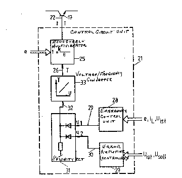
F.ig. 2 is a detailed circuit diagram of control
circuit unit 21, which sends, as described above, switch-on
interval signals t and period interval signal~ T to switch
17~ Unit 21 comprises a monostable multivibrator 25, an
error amplifier or controller 27, an emergency control unit
- : ,
: . ' '
1 31 29 1 7
2~" a priority circuit .~1 and a voltase/reql1ency ronverter
33~
Input ~7~1tage e is fed as a contro~. variable to
S monostable multivibrator ~5. Whenever a trigger .sig~al
arrives at input 2~, monostable multivibrator 25 is
aGtivated. Aftex a time interval where t=k/e, ~where k is a
Gonstant) multivibrator 25 reverts to its resting state.
Th.is sequence ensures that the product of e=t remain.s
~onstant, a condition that is advantageous for the overall
prior art Gontrol process. A multi.vibrator of the ahove-
mentioned type is also known, e.g. from the above--mentioned
Patent 08~/OOQ85. Control].er i.e. error amplifier 27 can,
for example, be embodied as a differential amplifier, to
which actual and referenGe voltages Uist and Usoll are fed,
while voltage~fre~uenGy converter 33 can be em~odied as a
commerGially availakle VCO (voltage Gontrolled osGillator).
Units 2~, 33 and 25 GOnstitUte a conventional and
known control cirGuit that serves to compare output voltage
Uist to reference value U5G11; deviations between these two
value~ are u~ed by the voltage/frequency converter 3.~ to
modify the length o~ period interval T. SwitGh-on interval t
meanwhile remain~ Gonstant, and are influenced only by th
~a.intly perceptible input voltage e that osGillates over a
2~ given period interval T.
It is proposed that an emeryency control cir~uît 2
operate in conjunGtion with this known control cir~u.tt.
'
1 31 2~ 1 7
Priority circu:it ~,1, ~hich, convention~lly, compri~Je~ two
diode~ and a resistor, release~ via it3 output 32 the greater
of two vo.ltage~ u~ and u2 which might arrive at it~ input.~ 2
and 80. Voltage u2; arrivin~ at the olltput of contro~ler 2
is, a~ a rule, greater than u1, a condition under]ying the
operation Qf such control circuit. 5hould, however, voltage
~list ~e significantly smaller than IJsoll, which alway~ oc~ur~
for a short interval when output voltage regulator 11 is
swit~hed on or for a longer period during a short-cir~uit a~
o~ltpUt terminals e,d, then voltage u1 has priority at the
output of emergency control unlt 28, and governs the
remaining process. Emergency control unit 28 hence prevents
the control circuit from operating under conditions that may
hamper the operation of this circuit. Fed through inductor
or choke 19 to emergency circuit 28 a~ control variables are
input voltage e, output vol-tage Uist and Gurrent il.
Fig. 8 shows a further-refinded cir&uitry arrangement
of emer~ency control circuit 28, which comprise~ an
~0 adder/sub~tractor 37, a multiplier/divider 40 and a
comparator 43. Adder/subtractor 3~ is, for example, embodied
as a differential amplifier. Input voltage e is fed to
control cirGu:lt 28 via input 35 while output voltage Uist i.
fed via the other input 36. Arriving at output 38 is a
si~nal corresponding to the difference (e-U) between the
above-mentioned voltages. I~suing from multiplier/dlvider
40, which can, for example, be a commercially av~ilable
1 3 1 29 1 7
- 7 --
çompQnent MPY lOo ~upplied by the ~.urr-P.rown çomp~ny, i 3 a
~ignal I that is proportional to ~e--U)/e and corresponds to a
current.
r~ Finally, in çomparatQr 43, sggnal 1 i.s çomp~red with
the preva.iling current il, pa~ing thrQugh çhoke 1~.
Comparator 43, em~odied for examp]e as a dlfferent:ial
amplifier, releases via output 44 voltage u1. The latter is
consistently greater than u2, if iL is greater th~n I.
In the emhodiment desçribed, analog emergençy control
unit 2~ continually extends, by means of it~ outpllt signal
ul, the duration of period interval T so as to ensure that,
during the next switch-on interval, the strenyth of current
iL flowing through çhoke 1~, çannot surpass a preset value.
As soon as it is established that this predetermined value
will not be exceeded, emergency control unit 23 yields its
governing function and control of output voltage Uist to the
ahove-mentioned control circuit (Unit~ 27, 33, 35).
Emergency control unit therefore remains in con~inuous
operation and reacts very rapidly each time the above-
mentioned predetermined value is reached.
Fig. 4a illustrates the time curve of current açross
Ghoke 1~, whereas Fig. 4b is a diagram of output voltage
Uist. The x axis is time, while the y axis is the current,
~5 or voltage. In every period interval T, switch 17 clo~es for
an interval that is almost a5 long as the next. During the
remainder Of each period interval T, .switch 17 is closed.
:
.
. : : . ~: .
1312917
~i .
While current irl inGreases, during switch-on interval
t cho'~e 1~ i9 loaded with energy. D11L ing the remainder of
the ~eriod, chol~e 1~ is partially disGharged and current ir,
suhsides. If the voltage rJist at loacl 15 remain~ cons~ant,
.it is reasonahle to assume that the length of period
intervals T will not fluctuate. Should at this point a
sudden short-circuit oc~ur at load 15, OUtpIlt voltage Uist
falls rapidly towards zero. The control circuit (~lnits 27,
l~ 3~, 25) is thus a~le to shorten the duration of periQd
interval T while Gurrent iL rises rapidly and steeply in
small increments. ~ef~re the permitted maximum current ima~
i~ ex~ee~ed duri.ng a given switch-on interval t; the
~m~r~el~y control unit intervenes at the end of the preceding
p~ri~ interval T and extends this interval T such that at
the end of the next provisionally delayed switch-on interval
t, the maximum current imaX is reached but not exceeded. The
lengths of t~e subsequent period intervals are then adjusted
in ~uch a way that at the end of each switch-on interval t~
~0 the maximum current imaX is reached, but not ex~eeded.
~m~r~nGy Gontrol circuit 2i~i thus constitutefi a type of
pre~i~tive ~ontrol that "predicts" in each period interval T
the size of the maximum Gurrent iL to occur in the fcllowing
Interva.l T. Should the predicted current strength he
R~ive, emergenGy control un-t.i 2~i intervenes to prevent
~h~ maximum allowahle current from heing surpassed.
.~ . .
. .
. .
-
:
1312917
The behaviour and construction of emergency control
unit 2~ a~ d~crihed in further detai] in ~ig. 5 which is a
furthe~ time GUrve correspond.ing to that of Fig. 4a. AlQn~
S the x-axi~ are arranged in ~eries two period interva]~ Tn_1
and Tn and their respective switch-on intervals tn_1 and tn.
~lon~ the y-axis are maximum currents jn_l and in at the ends
of their respective switch-Qn intervals tn_1, tn and the
minimum currents in-l and in at the ends of their respective
period intervals Tn-1, Tn~ or, rather, at the ~eginning of
each o~ the following period intervals Tn~ Tn~i. The cllrrent
fluctuates durin~ the swit&h-off interval ~T-t)n_1 occuring
~etween jn-L and in_L and during the switch-Qn interval tn
between in-1 and in~
1~ Due to the ~hortness of the intervals in the
timeframe under con~ideration, lnput voltage e and output
vQlta~e ~1 are to be regarded as constants. Concernin~ the
multivibrator ~S, t=e is constant. It ls required that jn
not exceed a predetermined m~xlmum current ima~ l.e. in~
~o ~me~x.
We can Gonclude from F.ig. S that
n=jn-l~(in-l-ln-l)+(jn=in-l) (L)
Ry app.lying the Law of Induction,
-in_L~e-u . tn (I,=inductivity of the choke 1~) (2)
a~ L
- :
,
.:: . . .
:
,
1312917
- 10 -
Since t.e= ~ ~=cons~), the eXpre~siQn i~
transformed into
n-l = in - e-u . ~f (3)
e L
This expression i~ realized by the circuit shown in
F.i~. 8 and indicates that, ~iven t.he minimum current value
in_1 of period interval Tn_1 and the knowledge of the Law of
Induction, it can be predicted whether or not, d~ring the
1~ subsequent period inter~al Tn~ the maximum allowed current
will he excee~ed~ If it is decided that this value will ~e
~x~eded, perlod interval Tn_l is extended until jn=e-u . ~r~
wh.~ch ensures that maximum current iLmaX is virtually reached
1~ at the end of the next switch-on ~interval, as Fig. ~ shows.
If input voltage e i5 Gonsidered to be constant at
its maximum value ema~l then expresaion:(S) c~n be reduced to
n-l = Jn ~ ~ = U . Qf. ~ (4)
L emax 11
2n The above expression i.ndicates:the maximum v~lue permltted
~r ~n-l, in order to ensure that current jn does not exceed
t~ m~ximum allo~ed current imaX.
Fig. 6 shows a further cîrcuit diagram o~ emer~ency
~ntr~l unit 28, which corre~ponds to expression (4.~. In
~S this verslon of emer~ency~control unlt~2A, units~37~and 40 of
Fig. 3 are reduGed:~tQ one analog~adder 50. :Fed to:the latter :
, ;
' ' ''" '.' . . ' ' ' " ' ' . '.' ''' . '
1 3 1 29 1 7
via input 51 is the variable output vol~age IJist and ~ia
inputs ~2, 5~, the CQnstants iLmaX and --~f; The ol.ltput signal
r~ I' of analQg adder 50 is, as Fig. 3 shows, Gompared by means
~f a comparat~r 43 to Gurrent iL. As soon as I' exceeds iL,
voltage ul at output 4A surpasses voltaye u2 at output 30 of
contrQller 2~/ at which point emergenGy control unit 2~
intervenes instead of priority 1QQP .1 to govern output
n volta e regulatQr 11.
The described method for preven~ing transients from
d~m~in~ nutput vQltage regulator (11) is simple and is
embod.ied as described in the manner of a predictive
controller. Su~h an arrangement permits swift reaction to
1~ very short transients and operatiQn in the presence of
perturhations of longer duration, su~h as short ~ircuits that
oc~ur at the output terminal. The switçhing arrangements
req~lired by the propQsed method, in particular those
~e~cribed in Fig. 61 are ~uite simple and can be GQnstruGted
.~ f~om commercially-available electr~nic COmpQnentS,
: . .
: