Note: Descriptions are shown in the official language in which they were submitted.
1312971
LOW POWER CONTROL ~PPARATU5 FOR
A COIN OP~RATED $ELEPHON~
This invention relates to control apparatu~ or coin
operated telephones. ~ore particularly, ~hi6 invention relates to
a low power controller ~pparatus having ~ single proce~sing
element which con~rols th~ aperations per~ormed by a co~n operated
telephone. Those operations ~ay include control of all the
functions of an electronic coin acceptor for accepting and
validating coinsl as well as all o~ the functions presently ~ound
in standard payphones. The present invention includes a unique
power distribution ~anagement system to ~ccomplish all these
functions while operating utilizing power ~rom the phone line.
~ackqround Of The Inven~ion
Coin operated telephone s~ations are in~er~aced with a
central office by a two ~ire loop circuit. When the ~andset is
lifted off the hook, the central of~ice ~upplies a very ~mall DC
loop current, 23 mA ~inimum, ~hich is available to the coin
op~rated telephone for use as a source o~ power. When the handset
~s on the hooX, the coin operated telephone draws virtually no
current fro~ the phone line. These extre~e limits on the power
available from the phone line have li~ited the func~ions that are
incorporated into coin oper~ted telephone stations.
"
1312971
T~e vast ma~ority o~ pr~ently existing coin operated
telephones or payphones are elec~ro~echanical in nature~ See, for
example, the ~Coin 5ervice Booklet~ publi~hed by New Yor~
Telephone. These payphones include ~n alectro~echanical coin
~echanism for tas~ing the validity ~nd deno~ination of coins and
a limited nu~er of operational Punctions and ~eaturesO
With deregulation of ~he t~lephone industry, payphones
including a nu~ber o~ electronic ~unct~ons and Peatures have been
introduced. These payphones have taken two ~pproac~es to address
the demand ~or ~dditional ~unctions ~nd ~eatures, and the
constraints of low power operation. In ~ome cases, one or more
advanced functions havQ been incorporated by using an internal
battery to supply additional power ~or performing these functions.
Other coin operated telephones have ~imply not incorporated a full
range of advanced function~. .
~ hile both the desirability and problems o~ having a
coin operated telephone ~tation which operates with very low
power, 6uch as the 23 ~A available from the phone lines, are well
known, the prior art has not successfully achieved ~uch operation
-in conjunction with providing a full r~nge of advanced functions
as described below.
SummarY Of The I~vention
As more ~ully described below, the present lnvention
provides a low~power control ~pparatus ~or a coin operated
telephone, which utilizes a battery ~or a li~ited range o~
--2-- .
~312~71
function~ such as operation of the real ti~e elock, monitoring
switohss "on hook" ~nd to power the ~lec~ronics to go ~of~ hook".
~or all other functions, the pr~en~ control pparatus utilizes
solely phone line power to power i~s various operations. In one
embodi~ent, control a~paratus according ~o the pr~ent invention
controls ~h~ operation of an electrsnic eoin acceptor ~or testing
coins. In particular, ~he control apparatu~ controls ~he
provision o~ power to the coin detection and t~st ~ensor~, and
~ny coin directing mem~ers, such 2S a ~olenold or an otherwise
~lectrically controlled and ~echanically operated coin routing
gate. Further, the control apparatus ~ncludes a processing
circuit for processing coin test data and other output signals
from the electronic coin acceptor.
In addition to providing processing support and control
signals for an electronic coin ~echanism, the present control
system may provide control of one or more of the ~ollowing
components and ~unctions~ A relayR control, (2) ring
detection, (3) a monitoring system ~or ~onitoring payphone status,
for example, has the coinbox been opened, (4) coin totalizer
control, (5) earpiece volume control, (6) long l~op, hort loop
detection to ascertain the quality o~ ~he line, (7~ detection of
microphone presence, in other words, has the handset ~een
~andalized, for ~xample, has it been torn from the payphone, (8)
control of the connection of ~raud prevention ~ilters in the
speech network, t9) modem ~ontrol and data transmission ~or
example, transmission o~ the status of security ~witches, or coin
1312971
data such as the number o~ coins ln ~he coinbox o~ th~ payphone,
and finally, (10) over~ll power ~anage~ent ~nd control Gf the
power ~witched to th~ various p~rt~ ~nd ~unctions o~ ~he payphone
and the controller ~o assure low p~wer op~ration. In the
pre~erred em~odimen~, control apparatus accor~ing to the present
invention controls all of ~he above co~ponent~ and Punctions in
addition to controlli~g ~he electronlc Goin acceptor. To achieve
~his end while utilizing phone line power, a nu~b~r o~ nov~l low
power circuits ~ave been devised as more ~ully described below.
Description 0~ The ~rawiaas
FIG. 1 illustrates a coin operated telephone connec~ed to a
central office by a two wire loop circuit;
FIG. 2 illustrates the upper portion of an ~lectronic coin
acceptor suitable for use in the coin operated telephone of FIG.
1 and in conjunction with the low power control apparatus of the
present invention;
FIG. 3 is a block diagram of a low power controller in
accordance with a preferred embodiment o~ the present lnvention;
FIG. 4 is a flo~ chart illustrating the steps perfor~ed by
the low power controller of FIG. 3 when proces~ing a typical
local call made with a coin operated telephone ~ncorporating that
controller;
FIG. 5 is a second flow chart ~llustrating the steps
performed by the low power controller of FIG. 3 when processing a
long distance call:
1312971
FIGS. 6-13 are schema~ic drawings illustrating portions of
~he preferred e~bQdimen~ o~ a ~icroprocessor bas~d low power coin
operated telephone controller circuit according to the present
invention;
FIG. 14 is a ~chema~ic dia~ram of ~ pre~erred ground lifting
relay circuit;
FIG. 15 ~s a schematic diagra~ of a preferred off hook
detector circuit;
FIG. 16 is a sche~atic diagram o~ A preferred power supply
circuit;
FIG. 17 is a ~chematic diagram of a preferred power supply
and power control circuit ~or controlling ~he power supplied to
the solenoid of a coin routing gate in the eleçtronic coin
acceptor of FIG. 2;
FIG. 18 is a schematic diagram of a preferred interface
circuit for interfacin~ the microprocessor of FIG. 6~ with coin
test output signals from the electronic coin acceptor o~ FIG. 2
and a long loop detector circuit;
FIG. 19 is a sche~atic diagra~ of a pr~ferred dual tone
multi-frequency ("DTMF") generator circuit;
FIG. 20 is a ~chematic diagram o~ a preferred coin totalizer
control circuit for controlling and ~nterrogating 2 ~tandard
escrow bucket o~ a coin operated phone;
FIG. 21 is a schematic diagra~ o~ a pre~erred speech circuit;
FIG. 22 is a schemati~ diagra~ of a pre~erred handset rsmoval
`" 1312971
detection circuit, and inter~ace c~rcuit ~or onnecting the speech
circuit of FIG. 21 to the ~ er circuits o~ FIG. 23;
FI&. 23 is a ~chematic diagxam o~ pre~erred fraud prevention
filter circuits;
FIG. 24 is a sche~a~ic diagra~ o~ a pref~rred ~onitor ~ystem
circuit_for ~onitQring ~yst~m gtatus lnpu~s ~uch as coinbox
removal, door openings, and bat~ery ~ailure,o
~ IG. 25 is 2 schema~ic diagram o~ a preferred ~odem circuit;
and
FIG. 26 is a schematic diagram of a pre~erred ringing detect
and ringing control circuit.
petailed ~s~riptiQn
FIG. 1 shows a coin operat~d phone 2 which is connected
~o a central office 4 by two ~ires, the phone lines, which are
referred to as the tip 6 and ring R. As ~hown in FIG. 1, phone 2
includes ~ handset 10 having a ~outhpiece 11 and an ~arpiece 12,
which are connected by a handle 13, a keypad 14, a coin ~lot 16,
and a coin return slot 18. When no~ in u~e by a cus~omer, ~he
~andset 10 sits in ~ cradle 19 d~pressing ~ ~pring loaded switch
20. When ~he hand~et 10 is in the position shown in FXG. 1,
SWitGh 20 i5 in its "on hook" position. ~hen handset 10 is lifted
out of cradle 19, switch 2 0 is no longer depressed and it is then
in its "off 2~ook" position. As is well known, the cerltral office
4 applies various D.C. voltage ~mplitudes and polarities on the
tip 6 and ring 8, ~rom which the phone 2 generates its ope~ational
~ 3 1 297 1
power when handse~ lO i o~ hook. As wlll ~e ~ur~her de~cribed
below, the varying DC vol~ages ~nd an ~C r~nging voltage are
interpreted by the phone 2 as providin~ operational com~ands for
con~rolling its operat1on.
~ ~hen ~andset 10 i$ on hook, ~he phone 2 draws
e~sentially no power ~rom the ~ip 6 or ring 8. As will b¢
described ~ur~her below, ~he phone 2 doe~, however, perfor~
bacXground te ting and 8~ monitoring ~n its ~andby s~ate
using a ~all amount o~ po~er from an ~nte~nal ~attery.
To originate a call, a customer picks up handset 10
thereby releasin~ the switch 20 ~ro~ its depressed position. The
phone 2 enters its off-hook ~tate, and ~egins to draw power from
the tip 6 and ring 8 to process the call. Next, the customer
inserts a sufficient number of coins into the coin slot 16 to
cover the cost of the call and dials the number he wishes to call
using keypad 14. The dialed number is transmitted to central
office 4 which connects the call. The customer'~ money is
collected by phone 2 when a collect signal from the central office
4 is rQceived. ~he custo~er completes his call and then hangs up.
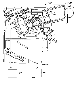
Turning to FIG. 2, the details of validation of a
customer's coin or coins will ~e briefly discussed. FIG. 2 shows
an electronic coin acceptor 30 suitable for use in con~unction
~ith t~e low power controller of ~he present invention.
Additional details o~ the operation of the preferred electronic
coin mechanism`for use ln ~onjunction Wi~h the presentation are
~ound in United State~ Applications Serial Nos. 188,038
-- 1312971
(~Jam Reducing Apparatus For ~e In A COiA Operated ~achinen) ~nd
lg9,138 ~Compact, ~ow Power Ga~e ~ppar tus For Coin Operated
~achines~) ~iled on April 29, 1988 and May 26, 1988 r~spectively,
and assigned to the a~Rignee of ~he prQgent inYention. ~he
disclosures of thes~ tw~ applications are ~ncorporat2d by
re~erenee ~erein.
In ~IG. 2, a cus~o~er's coin 3 1 i8 ~hown bein~ inserted
through coin slot 16 in ~ront panel 33 o~ the phone ~. From the
~lot 16, coin 31 tra~els past a plurality o~ Coin detectors and
sensors 34, 35, 36 and 37. After the last sensor 37, coin 31
falls onto a gate 38 which directs the coin 31 either to a coin
escrow bucket 39 or to a return chute 40 which directs the coin
31 to the coin return ~lot 18 where it can be retrieved by the
customer. In traveling fro~ 510t 16 to ~he coin ~scrow bucket 39
or the coin return chute ~O, coin 31 tra~els ~long either an
~ccept path A shown as a solid line in ~IG. 2, or along the raject
pa~h B shown as a dashed line in FIG. 2.
As will be discussed ~urther below, ~ach of the sensors
34, 35, 36 and 37 produces an electrical output signal Which
~erves as an input to a processing ~lement, which is prefera~ly a
microprocessor or microcomputer, ~hich detarmines ~hether khe
coin is an acceptable one and its denomination. The
microcontroller ~lso produces o~tput 8ignal5 for controlling the
position of the gate 33 50 that gate 38 either directs ~he coin
along path A o~ path B. The proCessing ~eans ~160 controls a
power supply for ~upplying power to energize the gate 3B. The
1312971
processing of ~he electrical output s~gnal~ ~rom the sensors 34,
35,.36 ~nd 37, the genera~ion of gate con~rol si~nals, ~nd the
control of the gate power ~upply are ~11 electrical control
functions performed ~y ~e low pow~r con~roller of the present
invention.
Referring to FIG. 3 of the drawings, a block diagram of
a 1QW power control circui~ 50 is illu~trated. ~ llne interface
circuit 55 co~prising a ground lifting r~lay circuit 160 and an
of~-hook detector circuit 190 connects the tip ~ and ring 8 lines
from the central office 4 to ~ power ~upply circuit 230. The
ground lifting relay circuit 160 also 82rv~s ~0 selec~ively
connect the tip and ring lines 6 and 8 to a coin totalizer control
circuit 350 comprising a totalizer relay circuit 355, a coin
supervisor detector circuit 360, a coin relay circuit 365 and a
first coin bypass circuit 370. The interconnection of coin
acceptor 30 of FIG. 2 which is responsible ~or acceptlng and
validating coins deposited in coin slot 16 o~ FIG. 1 is also
shown in FIG. 3. The coin acceptor 30 directs acoepted coins to a
standard coin telephone Qscrow bucket (not shown). This escrow
bucket holds the coins in escrow until comple~ion o~ the time
period for which the coins were d~posited and then collects ~hem.
based on commands from the central office 4 ~nd resulting control
signals produced by to~alizer control circuit 350. Coin acceptor
30 provides ou~put signal3 to processin~ element 100 ~nd in return
receives operational control inputs ~rom the processl~g element
_9_
.
`` . 13l297l
lO0~ Proc~s~in~ element 100 i~ ~hown in FIG. 3 as co~prising a
real ti~e clock 102, ~smory 104 ~nd a ~icrocontroller llO.
Returning ~o the power gupply eircui~ 230, that circuit
is shown in FIG. 3 as having oUtpUts connec~ed ~o a gate ~olenoid
power circui~ 250, a l5V power ~upply circuit 260, an~ an ~udio
netwoxk 380. ~ore ~peci~i ally, power ~upply 230 provides power
to a standard DTMF ~eypad ~hich ~ presen~ly prefesred for use as
th~ keypad 14 of ~IG. 1, a DTMF decode circuit 395 and ~ ~peech
network 390. With the ex~ep~ion o~ the li~tod ~unctions powered
~rom battery 511 which is part of a moni~or ~ystem 510, the power
supply circuit 230 in conjunction with control ~ignals ~rom
processing element 100 control~ the provision o~ all power for the
low power controller 50. Power for the coin routing gate 38 o~
the coin.acceptor 30 i5 pro~ided through pow~r 6upply 230, to the
gate solenoid power ~upply 250, and ~ro~ ~here to ~he gate 38.
Power for all the digi~al el~ctronic Componen~s requiring a SV DC
-eupply is pro~ided through supply 230 to the ~5V power supply
260. ~hen the audio network 380 i~ powered up, it provides ~he
phone 2 with the capability o~ trans~itting and receiving speech
and audio tone &ignals. These signals are transmitted and
received as AC voltages on the tip 6 and ring 8 which are offse~
by the DC ~oltage applied by the central o~fice 4. The processing
alement lO0 through its single microcontroller 110 controls all
the operation5 of phone 2 $ncluding audio network 380, coin
acceptor 30, and power supply 230. As Will be discussed rurther
below, microcontroller 110 also records the ~ta~us o~ the phone 2
-lQ-
1312~71
and has ~he capability of initiatlng co~municationS during the
stand~y mode i~ that status warrants it.
~ udio networX 380 comprises a large number o~
interconnected blocks under the control o~ ~icroaontroller llo.
~ore speci~icallyr ~he ~peech network 390 i connected to the
DTMF dQcode ircuit 395 and ~he DTNF kaypad 14. Further, the
~peech net~orX 390 i8 also connected to a coin tone generator
320, a DTMF generator 321, an audio bal~nce circuit 480, a first
switch 405, and notch ~ilter circuit 4~0. ~he DTM~ decode circui.t
395, the coin tone generator 320 and ~he DTMF generator 321 are
in turn connected to a ~odem circuit 400. ~ode~ circuit 400 is
also connected to the first 6witch 405 ~nd a ~econd switch 420.
The notch filter circuit 470 is connected ~hrough a low pass
filter (LPF) circuit 415 to the second ~witch 420. The s~cond
switch 420 is ~lso connected to a microphone in the mouthpiece 11
of the handset 10. First ~witch 405 is connected to a level
adjust circuit 410 which i~ in turn connec~d to an ear piece 12
of the handset 10. Handset 10 is further connected to a handset
detector circuit 430. The Dr~F decode circuit 395~ ~he coin tone
generator 320, the DTMF generator 321, the ~ode~ ~oO, ~he first
and second switches 405 and 420, the level adjust 410, the handset
detector 430, and the notch filter circuit 4~0 ar~ ~ll further
connected to microcontroller 110 and the ~onitor ~ystem 510.
As its name implies, the monitor system 510 ~onitors
the statu5 of ~he phone 2. Typically ~onitor ~yste~ S10 draws
its power from power supply 230 which is energized by power from
1312q71
~he tip 6 and ring ~ ~ines when ~he hand~et 10 i~ orS-hook.
Conseguently, normal operational power for ~oni~or clrcuit 520 is
provided fro~ the phone line.
~ aving ~ow introduced ~h~ ~arious block~ o~ luw po~er
controller 50, the operation of ~ho~e bloc~s will be discussed in
_
~he context Q~ ~he ~lswchartq o~ ~IGS. 4 and 5. FI~. 4 i~ a
flowchart of the opera~$o~ o~ controll~r So for ~ local call at a
fixed initial rate of 25 cents, ~nd FIG. 5 i8 ~ second ~lowchart
of the operation of controller 50 ~or a long distance call costing
in excess o~ the fixed initial rate.
Refarring to FIG. 4 of the drawings, the steps performed
by the phone 2 when proceRsing an initial rate call are
illustrated. An initial rate call is one which requires the
deposit of sufficient coins in ~he slot 16 to $atisfy ~he initial
rate for a local call from the phone 2. This rate is programmed
into memory in the phone 2 and may vary ~ith the location oS the
installation of the phone 2.
~ rior to ~tep 1000, in whic~ con~rol 50 enses that the
handsat 10 is off-hcok, the phone 2 is in the ~tandby ~ode,
perfor~ing background testing. The ~round lif~ing relay circuit
160 connects the tip 6 and ring 8 lines to the totalizer control
~ircuit 350 applying -48V DC ~hereto. ~e power supply ~ircuit
230 is e~fectively isolated from tip 6 and ring 8 ~o that ~he
phone 2 draws less than 1 microampere ~uA) o~ power.
Phone 2 enters the o~-hook ~a~e in step 1000, when
the handset 10 is removed ~ro~ its cradle 19 by ~ customer
1 31 2q7 1
d~siring to ~aXe a call. 8witch 20 1B th~r~by relea~ed Srom its
depressed position. With the hands~ o~f-hook, ground liftiny
relay circui~ 160 connec~s ~ip and r~ng vol~age throush the switch
hook fùnction circui~ 1~0 to power ~upply 230. The new position
of the switch 20 is sen~ed by the ~witch hook function ~ircuit
190 which t~l-ls ~he ~icrocontroll~r llO o~ the ~ew po~it$on over
a control line. Once charged, power ~upply 230 provides power in
~tep 1002 to ~icrocontrollQr 110 ~hich l~a~s it~ standby state
~nd performs a sequence o~ wakeup diagnostics. ~or e~a~ple,
microcontroller 110 interrogates h~ndset detector ~30 to learn if
the handset lO has been torn off, determines if au~io signals are
being produced by the ~T~F keypad 14, ~nd ~trobes coin detector
34 of coin acceptor 30 to determine i~ a coin is present or if
the coin entryway has been jammed.
The controller 50 is designed to operate with a phone 2
which operates in a dial tone first tDTF) mode. ~onsequen~ly, in
step 1004, rentral office 4 ~ransmits ~n electrical signal on ~he
tip 6 and ring 8 which is offset ~rom the DC voltage, so as to
produce a dial tone in the earpieca 12.
This dial tona ~ignal passes ~hrough ground lifting
relay 160, the off-hook detector c~rcuit 190 and the audio network
~80 to the earpiece 12. Assu~ing that ~he customer is not ~aking
a free call such as dialing an emergency number, ~or example 911,
the next 6tep 1006 o~ the ~lowchart of FIG. 4 is to deposit the
initial rate for ~he call, for example 25 cents~ When the
customer inserts a genuine 25 cents coin through coin 610t 16 of
-13-
.
.
1 3 1 297 1
~oin ~echanism 30, the coin fir~t p~e~ d~t~ctor ~en~or 34 whose
output ~ignal tells ~icrocon~roller 110 ~hat ~ coin or sbject is
present. The ~ensors 35, 36, And 37 ~e~t ~he coin'~ validity and
deno~inàtion. Since ~n our exa~ple, a genuine 25 cent~ coin was
inserted, ~icrocontroller 110 de~er~i~es that an acceptable 25 cents
coin has been inserted ~nd instructs gate 38 ts direct ~hat coin
to the coin escrow bucket 39.
A te~porary register ~tores ~he numb~r o~ coin~
accepted. A regist~r ~or ~ach possible coin denomination is
provided to store a running ~o~al o~ ~he number of coins of each
denomination deposited. Ano~her register is provided to store
the total number of coins deposited.
The acceptance of th~ Goins i~ conditioned on there
being sufficient power to power gate 38. This conditional
acceptance provides ~he advantage of not Gausing a ; a~ in the
coin acceptor in cases where ~here is in~ufficient power and
thereby avoids problems with ~uture USQ 0~ the phone 2. It also
avoids ~he loss of coins by a particular customer ~hereby avoiding
customer ~rustration ~nd ill will. Po~er to ~he gate 38 is
provided by rapidly charging a capacitor in the sate solenoid
power 6upply 250. Before the decision to aceept a c~in $s made
by microcontroller 110, the voltage across t~e capacitor is
checked. If in5ufficient power is sen~ed, the coin iB re~urned
to the customer by routing the coin to coin return slot 18.
Meanwhile, the dial tone continues until a nu~ber is
entered on the key pad 14 or until the central office 4 determines
14-
" 1 3 1 297 1
that no n~Eber has been en~ere~ for 20 ~econd5. Thisdeter~ination is ~ade ~ ep 1008. I~ a nu~ber 18 not dialed
wi~hin ~he allotted ti~e, ~he central o~ice 4, at step lO09
instructs the call~r to hang up to reacgulre the d~ 1 tone. If
the caller hangs upt phone 2 rQturns ~o ~e utandby mode. Then,
if the caller ~gain picks up ~he handset 12, ~he cycle begin~
again ~t step 1000.
~ t step lO0~, the caller dial~ ~ number using DTMF
keypad 14, the keypad ~o~h monitors the numbers dialed nd
generates a dual tone ~ignal for each nu~ber depressed. These AC
signals are offset from the DC voltage and are transmitted through
the tip 6 and ring 8 lines. The DTMF ~ignals infor~ ~he central
office 4 of the desired telephone number.
During the dialing of ~he number, the DTMF decode
circuit 395 monitors ~he DTMF signals generated by the DTMF ~eypad
14. As part of a call accounting package, the called number is
stored ~or each call.
Once a valid number has been ~ntered on the ~eypad 14,
the central office 4 in step lO10 tests the totalizer relay 355
to see if the correct deposit of the initial rate ~or a local
call ha5 been ~ade. For a free call, the cen~ral o~fic~ 4 returns
any deposited coins. A valid number ~ay be as ~hort as one digit,
such as "zero" ~or operator, or as long as Qleven digits. The
central office 4 tests the phone 2 for deposit of the ~nitial
rate by momentarily removing ;~4BV from the ring 8 nd ~pplying it
to tip 6. Electronic sensor in the power supply 230 ~ense the
-15-
1 3 1 297 1
~omentary interruption o~ voltage and ln~orm the ~$~rocontroller
110 of ~his interrup~ion. Th~ ~icrocon~roller 110 then polls the
~witch hook ~unction circait l9Q to ~iscover why pow~r to the
supply~ 230 wa~ interrupted. Two r~ason~ are po~ ible. First,
the handset 10 could hav~ been retu~ned to it8 hook po~ition by
~he caller.... Second, ~he central o~fice ~ could be performin~ a
test. Switch hook ~unction circui~ 190 senses the position of
~he ~witch 20 and informs ~he ~icrocontroll~r 110 ~hether ~he
handset 10 is on- or o~-hook. Fro~ ~his data, ~icrocontroller
110 can readily determine the reason for the absence o~ voltage.
Where a central o~f~ce t~st iB being ~ade, micro-
controller 110 causes the ground lifting ~elay circuit 160 to
switch to connect ~he tip 6 and ring 8 ~o the totalizer control
circuit 350. With ~he central office 4, applying 48 volts DC on
the tip 6 and grounding the ring 8, coin ~upervisor 360 senses the
voltage polarity and level on the tip 6 as referenced to ground
and determines that ~he c~ntral o~fice 4 is testing for the
correct initial deposit.
If the correct amount has been deposited, a contact
will have been closed in the totalizer rel~y circuit 355. The
coin supervisor 360, ~f it senses this clo~ied contac:t c:auæes an
electrical signal to be placed on the tip 6 indic?tive of the
~eposit of the initial rate. No such signal is generated if the
contact is open.
The ground liftin~ relay circ:uit 160 rec~nnect~ power
through the switch hook ~unction detector 190 to power ~upply
-16--
t312q71
2300 During the ini~ial rate test, power 3upply 230 was not
energized. To ~ee~ the pow~r de~ands of the microcontr~ller 110
during this time, ~ capacitor with a charge stored while the
power ~upply 230 wa~ previou31y ¢nergized, 18 di~charged.
~ her~ ~he initial rate test ~tabllshes that ~n adequate
deposi~~has been made, ~he call is placed in step 10120
Otherwis~, in step ~013, a recording in~truct~ the customer to
reinitiate the call with the proper initi~l depositO
After the called third party ~nswers, the central of~ioe
4 initiates timing o~ ~he call. Th~ call continues until ~he
initial period ends. Then, the central of~ice 4 causes, in step
1014, the phone 2 to collect the coins in the escrow bucket 39
causing them to ~e delivered to a coinbox (not shown) which is
located behind ~he coinbox door 21 o~ FIG. 1. Coins ~r~ collected
from the coinbox by using a key in keyhole 22 of FIG. 1 to open
the coinbox door. Preferably, the opening o~ the coinbox door 21
actuates a status switch which is ~onitored by ~he con~roller ~0.
To collect coins, central o~fice 4 r~moves the ~oltage
at the tip 6 ~nd ring 8, and then ties the ring 8 to tip 6 and
applies ~130 volts DC relative to ~ar~h ground. The power supply
circuit 230 senses the interruption i~ voltage and ln~orms the
microcontroller 110, which causes ~he ground lif~ing relay circuit
160 to connect the 130V s~gnal to the coin relay 365. m e coin
supervisor 60 sènses this voltage and as a result causes the
collection of ~he coins.
131~971
If the call had not been placed a~er the initial r2lte
was deposited, ~che cen~ral o~f ice ~, would ha~e caused t2~e phone 2
to refund the coins in step ~016. This refund woul~ be made by
removing the voltage on the tip 6 and r$ny 8, and ~hen tying ~he
ring 8 ~o the tip 6 and applying -130 volts DC relative to ~arth
ground.
~ r~or to ~xpirat~on of the initial r~te period, ~he
custo~er is instructed ~o deposit additional coins for overti~e
usage in order to continue the call. ~he c~ntral office 4,
sensing that ~he call is continuing a~ter a predetermined time,
tests for the presence of ~he necessary overtime usage coins in
step 1017. As was the case in testing ~or the initial rate
deposit, the central offic~ 4 applies +~8 Volts DC to the tip 6
and grounds the ring 8 to ~est ~or the pr~sen~e o~ the necessary
dQposit escrowed in the coin escrow bucket 39 by testing coin
relay ~65. The coin upervisor 360 senses this test ~nd replies
with the result. If an adequate deposit has been ~ade,the caIl
continues in step 1017, otherwise a recording or an operator is
connected which ~akes a request ~or the overtime deposit in step
1019. Finally, i~ the overtime deposit is not ~ade, the call is
disconnQcted in step 1020.
Upon completion or ~bandonment of ~ call, ~he customer
hangs up th~ handset 10 returning it to the on-hook position.
The ground lifting relay circuit 160 connects the tip and ring
lines to the coin reiay 365, as discussed previously, ~nd the
central of~ice 4 interrupts voltage on the ~ip 6 ~nd ring 8 and
--lS--
- 1312971
~pplies a collec~ ~ +130 volts DC; or a re~und ( ~130 volts DC)
voltage with respect ~o ground to ~he tip 6. The phone 2 either
collects or r~funds the coins as instruGted, and ~hen returns to
~he ~tandby ~ode.
During the ~teps ~llustrated in FIG. 4, ~he audio
network 380 pro~ides an interface for ~udio ~iqnals between the
tip and ring lines ~nd the ~ou~hp~ec~ 11 ~nd ~arpiece 12 in ~he
handset lO. ~he ~peech n~twork 380 al~o l~it~ no~e to ~he
earpiece 12 during the ~equence described above ln connection
with discussion of power up step 1002.
Audio sisnals from ~he central of~ice 4, representative
of speech are imposed on the tip 6 and rin~ 8 offset from any DC
voltage present. Those signals propaqate ~hrough the ground
li~ting relay circuit 160 and the switch hook ~unction sensor
190. The sensor ~9O passes the ~ignals to the power ~upply 230
and then to the audio network 380. The ~udio network 380
processes the signals providing isolation between the ~outhpiece
11 and earpiece 12. The processed signals go
through the first switch 405, and the level adjust ~ircuit 410 to
the earpiece 12 where the signals are converted to audible
signals. The level adjust circuit 410 provides four levels of
audio signals which can ~e selected by a ~witch 23 on the handset
10 which causes a circuit in the handset detectQr circui~ 430 to
have differing resistances according to the number o~ ~ctuations
of the 5witch 23. The ~ic~ocontroller llO controls the level
adjust circuit according to the resistance in the h~nds~ detec~or
-19-
1 3 1 297 1
circuit 430, ~hereby controlling ~he ~i~nal level in the earpiece
12.
During voice trans~ission ~ro~ ~he phone 2 to ~he
central o~fice 4, a call~r ~alk~ in~o ~he ~icrophone of mouthpiece
11. ~he ~icrophone ~onverts ~h~ Yoic~ ~ignal ~nto electrical
signals which are p2~sed through ~he ~cond switch 420 to the low
pass ~ilter and prea~plifier circuit 415. ~he ~econd ~witch 420
selects between th~ ~icrophone and th~ ~ode~ ~00. ~he ~ignal
from the circuit 415 ~hen passes through a 2600 ~z notch ~ilter
in filter circuit ~70. The 2600 ~z ~ilter ~ay be ~ele~tively
switched in and out of the circuit under the control of the
microcontroller 110. Th~ filtered ~ignal from the output of
~ilter circuit 470 is processed by the ~peech network 390 and
output to the powex ~upply 230 where it is offset fro~ the D.C.
voltages present in that circuit. The o~fset signal is passed
through the switch hook unction circuit sensQr 190, ~hrough the
ground lifting relay circuit 160 to the phone lines.
~ ~raud audio balanc~ circuit 480 is provid~d to prevent
detection o~ the 2600 ~z notch filter by one at~empting to commit
fxaud with a tone generator. ~ er detec~ion is possible because
the speech network 390 provides ~ide tones, which ~eedback some of
the electrical signals generated ~rom the microphone into kh~
~a~piece 12 to pr~vide a natural volume refarence for the Galler.
WhQn the 2600 Hz filter is ~nserted into the trans~ission path,
in the absence of balance circuit 480 it is.possible to detect its
presence by a change in what i5 ~eard in thQ ~arpiece 12. This
-20-
1312971
change occurs because the raudulent tones ~re ~ilter~d out and
not heard in ~arpiec~ 12~ T~e Sraud audio balance cir~uit 480
provides an alterna~e au~io path so ~hat the ~raudulently
generated tones are h~ard ~n ~arpiece 12, and con~equently, a
person cannot ~mediately detect the pr~enc~ 9~ ~he 2600 ~z notch
~ilter.
Referring to FIG, 5 of ~he dr~wing~, ~he ~teps performed
by ~he phone 2 when ~ call requir~ng ~ore ~han ~he initi~l rate is
placed, are illustrated. The phone 2 ~ollows the ~ame procedures
in steps 1040, 1042, 1044 and 1048 a~ in steps 1000, 1002, 1004
and 1008, respectively of FIG. 4. ~t khe end of 8t~p 1048 when a
valid number has be~n dialed, ~he central office 4 dete~mines
that the nu~er dialed reguires more than the initial rate and in
step 1050, refunds any cnins whic~ have been deposited in the
phone 2. The re~und procedure is ~he ~ame as described in step
1016 of FIG. 4.
The call is then connected to ~ither a Traf~ic Service
Position System ~TSPS) trunk or ~n Automatic Co~puterized
Telephone System tACTS) trunX in 3tep 1051.
In step 1052, the central o~ice 4 re~erses the polaxity
on the tip 6 and ring 8. The power supply circuit 230 senses this
r~versal of polarity ~nd in~orms ~he microcontroller 110. TSPS or
~n AC~S trunk ~s connected to the phone 2 for a long distance
call~ The microcontroller 110 then disables ~he aTMF key pad 14,
and disconnects the 2600 Hz filter. It enables the coin tone
generator 320 and conne~ts a ~eoond ~ilt~r, ~ 2200 Hz ~otch
1 3 1 297 1
filter, found in ~he ~ilter clrcuit 470. The 2200 ~z ~ilter
which is then in the line with the ~icrophone preve~s any 2200
Hz ~ignal ~rom reaching ~he tip 6 ~nd ring 8 ~ro~ ~he microphone,
thereby preventing the *raudule~t practice oP ge~erating tones at
the mou~hpiece 11 to si~ul~te ~he tone gen~rated by ~Ae coin tone
~enerator 32Q~
In step ~053, ~he TSPS operator reguests ~he deposit
required for the ~nitial call period P~r ~he nu~ber dialed. Coin
tone generator 320 ge~erates a unique dual tone signal for each
denomination o~ coin deposited in the coin ~lot 16, one of the
tones for ~ach denomination is 2200 ~z.
The TSPS or ~he ~CTS monitors ~he tones generated by
the coin tone generator 320 2nd determines the amount of coins
entered. Once the TSPS or the ACTS has deter~ined ~hat sufficient
coins have been deposited, the polarity on the tip 6 and ring 8
is reversed back to normal in step 1054. The ~icro~ontroller 110
disconnects the 2200 ~z notch ~ilter and reconnects ~he 2600 Hz
filter. The call duration is timed by ~he TSPS or the ACTS. ~he
call continues in step 1056 until the initial charge period is
completed. Then, $n step 1058, the coin are collectad ~y
momentarily removing ~oltage at the tip 6 and ring 8 and then
applying a +130 Yolt DC pulse, ~s pxeviously described.
During the standby mode, the phone 2 performs a sel~
diagnostics routine. The monitor ~ystem 510 examines the status
of the phone 2 by monitoring the real time clock 102, ~he batt~ry
level of battery 511 and a number of security ~witches represented
-22-
1 3 ~
by block 514 of ~IG. 3. The ~ecurity ~witches include one to
indicate removal o~ an upper housing o~ phone 2, 3 ~econd ~o
indicate the removal o~ the coinbox, and a third ~Aat d~tects the
opening~ of ~he coi~box door 21.
~ hen necessa~y, t~e ~onitor sy~tem S10 initiates an
internRlly generated o~-hook ~ondi~ion, $0 that ~he phone 2 ~ay
be powered up to place a phone call without ~he handset being
physically off-hook. Upon power up, the ~icrocontroller 110
interrogates the ~onitor ~ystem to de~er~ine what event yenerated
the ~ower up. The microGontroller 110 ~hen causes ~he ~irst and
second switches 405 and 514 respectively to ~witch the handset 10
out o~ the audio network 380 and to the modem 400 in line. Th~
microcontroller 110 then controls the fflodem 400 to transfer data
from phone 2 to the central office 4.
The power management in the phone 2 is important to
allow a large number of ~unctions to be formed utilizing powar
only from the tip 6 and ring 8. At the ~inimum line current, only
23 mA of current can be drawn from the phone llnes, 80 ~hat any
electronic implementation of a coin operated phone ~hat uses
power from these lines i~ normally 3everely li~ited by ~his ~mall
loop c~rrent. Controller 50 overco~es these li~tat~ons by
~mplementing a number of energy ~anagement hardware and ~oftware
technigues~
Controller 50 uses low power de~ices where availa~le.
Interfacinq is done through open drain CM9S devices. All parts
of the circuit peripherals can be turned off when not required to
" 1 3 1 297 1
conserve energy. All ~utually exclusive events or proces~es are
locked out by hardware and ~of~ware. The microcontroller 110
monitors tha ~otal power available and lncludes ~eans to direct
~he total available line power ~o a p~rticular ~unction. Upon
first receiving power ~ro~ ~he tip 6 and ring 8 upon power up,
power is allocated to rapidly charge energy ~torage devices, in
particular capacitor. ~11 the power ~ro~ the tip ~ and ring 8
charge ~he~e capacitors ~or a ~hort per~od Or ti~e. ~her~after,
indi~idual circuits are powered as power is needed. After a
~rief initial charging period, the microcontroller 110 and audio
network 380 are powered. The DTMF decoder 395 and the DTMF
generator 320 are powered only when needed. ~pon de~ection of the
depression of a button on ~he D~MF key pad 14, power is switched
to these circuits. The coin acceptor 30 draws a ~Dall a~ount of
current all the time, $n the off-hoo~ ~tat~. Its detector sensor
34 constantly ~onitors a coin chute, 80 ~ha~ ~hen a coin is
inserted into coin acceptor 30 ~t is promptly detected and, then
the remaining circuitry of coin acceptor 30 is powered up. Upon
coin detection, ~ capaci~or in gate solenoid power ~upply 250 is
rapidly charged. The speech network 3~0 is momentarily powered
down during coin ~cceptance ~s it ~s not needed. ~hen the ~p~ech
network 380 is required to generate coin tones, it is powered up
and the coin acceptor 30 is pcwered down. ~no~her pow~r control
feature is that the power supply 250 for the gate solenoid is
monitored. If~the voltaqe is not high enough, coln acceptor 30
will not accept coins. This is particularly useful where the
-2~-
1312971
phone 2 is located at ~he ~nd o~ a lon~ loop. In ~uch cases, ~he
rat2 of coin acceptance ~ay have to be ~lowed to allow time ~or
the gate solenoid power ~upply 250 ~o recharge. ~nder ~arginal
conditions, coins Will not be ~ccept~d.
Potentially high power ~tili2ation devices ~lthin
controller ~0 are t~e DTMF decoder 395, the D~F keypad 14, the
coin ~cceptor 30, ~he ~peech circui~ 390, ~he ~ode~ 400, ~ ~ervice
display (not ~hown) and the ~ilter 470. Th~ ceypad 14
generates a pair o~ tones when one of its buttons is press~d.
Circuitry is provided ~o disable the keypad l4 a~ter a half-second
of generation of tones, thereby limiting ~he maximum power ~rawn
by ~he keypad 14, and preventing intentional and unintentional
power dissipation by holding down a button for an extended period
of time. The modem 400 is only powered up during a required
modem call. The service display is only powered up during the
service mode in which a serviceman is repairing or chec~ing the
phone 2. The ~ilter circuit 470 ~ay also be powered down when
not in use. The ~onitor ~ystem 510 provides backgroun~ checking
for the status of phone 2. It is powered by a battery 511 so it
can continuously monitor the ~ystem. It ~onitors ~ecurity
switches, which include a ~witch ~or the upper housing, ~ switch
indicating that the coinbox has been re~oved, ~nd a 5witch
indicating that the coinbox door 21 has been removed. It also
~onitors the internal battery level, the real time clock 102 and
maintains memory 104 i~ the power lines are disconnected.
-25-
1 3 1 2q71
The con~roller o~ FIG. 3 ~or a coin operated phone, in
accordance wi~h ~he pre~arred e~bo~iment, i~ con~truted on two
printèd circuit boards~ The circuit on ~he~e two boards $ncludes
the lin~ i~terface circuit 55, ~he ~udlo ~etwor~ 3~0, the process-
ing el~t 100, and the power supply 230. The electronic coin
acceptor 350 functions are i~plemented on a separate printed
circuit board.
Circuits which i~plem~nt ~h~ processing element loo
(FIG. 3) in accordance ~ith a preferred embo~iment o~ ~he
invention are illustrated ln FIGS. 6~ through 13. Referring ~o
FIGS. 6A, 6A~, 6s and 7, the prwessin~ element 100 includes a single
microcontroller 110, its ~ssociated ~emory 104A and 104B, a real
time alarm 102, inter~ace circui~ry for the address and data
buses as w~11 as other interface circuitry~ Th~ microcontroller
110 selected is an 80e31, ~anufactured by Intel, although any of
the available ~icrocontrollers or ~icroprocessors can be used.
The 80C31 is a low power device, which perfor~s the controller
functions previously discussed. I~ is drive~ by a 3.6864 MHz
crystal Yl (FIG. 6A).
FIG. 6B shows 256X x 8 programmable read only memory
(PROM) 104~ which stores ~he op~rational program for the
controller o~ a coin operated phone as well as any constants
needed. The PROM used is a 27C256, available ~rom ~everal
manufacturers such as Intel. A 256k x 8 rando~ access ~emory
(RAM) 104B is provided for ~toring results ~ncluding the number
-26-
" . . .
1~12q71
of coins collected, ~he phone numbers dialed, ~tc. Like thRo~her circuitry, it ~5 powered fro~ ~he phone line volt~ge on the
tip and ring, however, bat~ery ~oltage i8 al80 available at its
power pin ~o ~hat there i~ a backup vol~ge ~n case o~ a power
~ailure during the phone c 11. The RA~ u~ed is ~ TC5~257,
~anufactured by Toshiba.
The 80C31 ~icrocontroller 1~0 ~as four I~O ports. Port
2 provides the high ~ddress ~us, AB-~15. Port 0 proYid~s a
multiplexed data bus DB0-DB7 and a lower ~ddxess bus AOoA7.
Registers U23 and U7 of FIG. 6A'latch the high ~nd low address
buses, respectively, ~t the appropriate tim~s. Transceiver U24
of FIG. 6A provides a buffered data bus inter~ace.
Ports 1 and 3 of the ~icrocontroller 110 are utilized to
provids an interface for other functions o~ the coin operated
phone to the microcontroller 110. For example, the following
lines transmit data to and from the coin ~cceptor 30 to the
microcontroller 110: ~CH C~OCX, ~EC~ D~TA, LF COUNT, J~ SENSOR
l-~AR, and JAM SENSOR 2-BAR. Other inter~ace llnes to the
microcontroller 110 from the controller circuitry include the
following signals SDA, SCL, RXD, TXD, ~ESET-~AR, INT0-~A~, RESET,
+48VDCT/PADEN, Ell/PAD/S, ~ODEM ENABLE, MUTEJKEY DEP, POWER DOWN,
and CARRIER DETECT.
FIG. 7 ~hows more interface circuitry ~or the
~icrocontroller 110. Decoders U10 and ~11 decode ~everal o~ the
address bit6 ~rom ~he ~icrocontroller 110 address bu~ to provide
read pulses (AORD-BAR to A7RD-BAR) 112 and write pulses (AOWR to
-27~
1 3 1 297 1
A7WR) 114 for ~he various circuits which interface with the
microcontroller 110.
FIG. 8 shows another interface carcuit ~or the
microcontroller 110. ~egi~ter ~13 l~ches data fro~ ~he buffered
data bus under control of the write pul~e, A3WR. The latchsd
data is ~ored by ~he re~ister ~13, who~e outputs remain high due
to pull up resi~tor~ R3s ~o R44 and R118, until ~nabled by ~he
line ~ESET from the microcontroller ~lO. Once enabl~d, the
outputs of the rsgister U13 are driven o~f the printed circuit
board through the connector P2 ~o the coin acceptor 30.
Figs, ~ and 9~ illustrates a clr~t:havi~g status and control
registers for the microGontroller llO. Registers U14 and U15
latch data ~rom the bur~2red ~icrocontroller data bus w~en write
pulses A6WR and A4WR, respectively~ are asserted. The outputs of
registers U14 and U15 are groups of con~rol signals 116 and 118,
which are enabled by the ~ignal RESET from the microcontroller
110. Buffers ~16 and U17 provide ~tatus read registers for-the
microcontroller 110. Data ~rom buffer ~16 is ena~led onto ~he
data ~us ~y a pulse on A2RD-B~R, allo~ing ~he ~icrocontroll~r 110
to read DTMF signals, 80 that $t can fulfill ~ts call accounting
~unctions. Data.~roD buffer ~17 ~s enabled on ~he data bus by a
pulse on A3RD-BAR. The ~icrocontroller 110 reads the state of
the DC ~oltage on the tip 6 ~rom this buffer 50 as to determine
what function the central office 4 w~nts performed.
FIG. 10 Rhows more status and control regi ters.
Register U17 latches data on the data bus when ~he write pulse
-28-
-
1312~71
AlWR is ass~rted and ou~puts the groups of contxol ~ignals 120
and 122. Con~rol ~ignals 120 eontrol the ~pplication of power to
various components in ~he coin operated phone 2. Data ~rom buf~er
U18 is enabled by AlRD-BAR when ~h~ microcontroller 110 wants to
read the st~tus lines illu~trated.
FIG. 11 illustra~es a circuit that monitors the ~oltage.
Co~parator U2B ~as a reference voltage, VCRE~, as one input and
the 4 volt DC signal through a resistor networ~ as ~he o~her
inpu~. When the resistance divided 4 volt signal ~alls below the
threshold value VCREF, POhER FAIL is ~c~i~ated~ This output is
fed through a buffer to the microcontroller 110.
FIG. 12 shows a switching regulated power ~upply.
FIG. 13 illustrates a tip to ring polarity ~ensing
circuit. Comparator U2A has th~ voltage on TIP 6 as one input and
a reference voltage, VC~EF, which is lower than ~he voltag~ on
TIP 6, as its other input. Whe~ the voltage on ~IP 6 ~alls below
the reference volta~e, which is always positive, it is necessarily
n~gative. The output of the co~parator! +48~DCT/PADEN, is
activated and fed directly to a port o~ the ~icrocontroller 110,
so that ~he polarity of the voltage on the TIP 6 c~n be
determined. The sensing of the polarity is done on the input
side of the polarity guard, ~o that there are no ~oltage drops,
thereby conser~ing energy.
The devices in FIGS. 6A through 13, which are used in
the preferred e~bodiment to imple~ent the proc~ssing element 100
-29-
- - -
1312971
(FIG. 3), are listed in Table 1 and are ~nterconnected as
illustrated in ~he drawings:
TABLE 1: DEVICES IN ~IGS. 6A ~hrough 13
Produ~t No.
~2vi~e or Val~e Prawinq R~e~e~
Micro~ntroller ~OC31 110 in FIG. 6A
Regist2r ~ 74HC573 ~7, ~23 in FIG. 6A: U13 in
FIG. 8; ~14-17 in FIG. 9, U17
in FIG. 10
Transceiver 74~C245 U24 ~n FI~. ~A
Gate 74~C05 ~3A, B, D, E in FIG. 6~; U3C
in FIG. 6B
Gate 74C906 U4A-E in FIG. 6~; U14A-C, F,
~4E,F in FIG. 8; U5B-F, U25F
in FIG. 9; U2B ~ D FIG. 11; U2A
in FIG. 13
Comparator LP339 U2C in FIG. 6A;-
Crystal 3.6864 MHz Y1 in FIG. 6A
32.76 kHz Y2 in FIG. 7
PROM 27C256 104A ~n FIG. 6B
RAM TC55257 104B in FIG. 6B
Gate 74HC03 USB in FIG. 6~; V5A, C in FIG.
Decoder 74HC138 U10 in FIG. 7
74HC238 Ull in FIG. 7
Clock S8167A U12 in FIG. 7
Buffer 74HC540 U18 in FIG. 10
Regulator ~X 631XESA UI5 in FIG. 12
Resistor Network lOOk RNl, 2 in FIG. 9
Resistor lM R13 in FIG. 6~ R60 in FIG. 13
200k R4a in FIG. 6A
68k Rll in FIG. 6A: R81 in FIG. 11
22k R18, 20, 10~ in FIG. 6~;
R24, 106-107 i~ FIG. 6~
Resis~or lOOk Rl~-5, 8, 10, 120, 14-17, 19,
22, 10~-115 in FIG. 6A;
R21,23,3~-3~ in FI~. 6B; R2g-30
in FIG. 7; R39-47, 117-118 in
FIG. 8; R86, 88-92 in FIG. 9;
R84-88 in FIG. 10; R8~-83 in
FIG. 11; R48 in FIG. 12; R57-
59, 61 ln FIG. 13; R6 7 in
FIG. 6A: R89-105 ~n FIG. 10;
' R50 ~n FIG. 12
100 ~9 in FIG. 6A
Capacitor lOOuF C35, 37 in FIG. 12
47uF C32 ln FIG. 8
-30
.
.
1312971
lOu~ C24, 27, 41 in FIG. 6A; C28 in
FIGo 6B
O.~uF Cl-2 in FIG. 6A: ClS ln FIG. 12
0.047uF C3, 4, 7, 23, 42, 43 in FIG.
6A; C8, 9 in FIG. 6B; C5, lo,
11 in ~IG. 7: el3 ~ 14 in FIG.
8; C14-18 ln FIG. 9; C17-18 in
~ FIG. 10: C38 in FIG. 13
0.001 uF C3~ ~n FIG. 12
30 pF C25-26 ~n FIG. 6A
~ ~- 20 pF C30-31 in FI&. 7
Inductor - 330uH Ll ~n FIG. 12
Diode N~DB914 D11-15, 18 ~ FIG. 10; D6-7 in
FIG. 13
~` BAT~7 ~3 ~n ~IG. 12
Transistor ~FRsO20 Q13 in FIG. 9
~MBT3906 Q4 in ~IG. ~0
FIG. 14 illustra~es a circuit in accorda~ce with a
pre~erred e~bodi~en~ o~ ~he invention ~hat implements the ground
lifting relay 160 ~FIG. 3). The circuit includes ~he devices
listed in Table 2 which are interconnected as illustrated.
TABLE 2~ DEVI OES IN FIG. 14
.
Product No.
nQvice 5~
Relay SPDT ~ 2~ ~S
Transistor ~MBT3906 Q7010, Q15-16
~MBT~9 2 Q5-6
Diode $~PD283~ D23-24, D27-29
lN4 004 D13-14
RI: 82P D12
Resistor lOk R73-74, R77~78, R83-84
3.3k R76
510 - ~72,75
A circuit implementing the 3witch hook ~unction detector
circuit 190 of FIG. 3 is ~llustrat~d in FIG. 15. q~he circuit~
-31-
:
1 3 ~ 297 1
include~ the devices listed i~ Tahle 3 ~hlch ~r~ interconnected as
illustrated.
TABLE 3: DEVICES IN FIG. 15
Product ~o.
~evice _ Ç~_Y~l~c r:~Yl~9L~5 ~L~/
Relay SPDT R3
Transistor ~BT3906 Q11, 12
Diode ~MPD2836 D25, 30
Resistor lOk R79-80
FIG. 16 illustrates a po~er ~upply circuit 230 that
generates approximately 4 volts on its ou~put 232 as a ~upply of
volta~e for the operational components of ~he coin operated phone.
The circuit co~prises the components li~ted in Table ~ which are
interconnected as illustrated.
TABLE 4~ DEVICES IN FIG. 16
Product No.
~evice or =alue_ ~awinq Refe~ence
MOV ~V1
GYRATOR ~1081 U10
DIODE ~MB2-5250B Dl, D2
1~5818 D3-6, 8
RESISTOR 13 R29
lOOk . R35-36
620 R37
CAP~CITOR 27pF C29
68pF Cla
4.7uF, tantulu~ C30
The power supply circuit 230 includes ~ polarity guard
234, which is constructed ~ro~ ~our diod~ D3-D6 that are arranged
in a full bridge circuit. Schottky diodes, having ~ low ~orward
~32-
'
1312971
voltage drop, are us2d ~o ~ini~ize ~he loss of voltage lnherently
associated with diodes, ~ereby, con erving power. These diodes,
however, have a low reversè ~reakdown ~oltage, typically 20 volts
~axi~um. ~he line voltage on ~he loop acro~s ~he t~p 6 and ring 8
is typically ~/- 48 vol~c. me coln operated phone pulls that
voltage down to ~ range o~ 4 to 8 ~olts ~hen in operation. There
is, however, a short t~me a~ter turn on vhen ~h~ diode bridge 234
is exposed to the full line voltage, thereby æxpo6ing the diodes
D3-D6 to a voltage that exceeds ~heir r~verse ~reakdown rating.
To overcome this problem, a pair of ~ener diod~s Dl and D2 clamp
the line voltage across TIP 6 and R~ ~o ~/- 12 volts, ~hereby
li~iting the maximu~ voltage acro~s the dio~s D3-D6 in the
polarity guard 234. The use of Schottky diodes in this circuit
offers a significant power ~avings over the conventional ~ethod
of using conventional diodes with a ~orward voltage drop which is
three times-higher but with: a sufficient reverse voltage rating.
The output of 'che polarlty guard 234 provides gyrator
U10 with a positive signal, regardlesc of the polarity on the TIP
6, through series resistor R29. T~is ~ignal has a DC component
as well as an AC component consis~ing of sp~ech and audio tones.
The gyrator U10 ramoves the AC components and outputs
approximately 4 volts DC w~ich provides power to ~he components
in the controller.
F~G. 17 shows a cirouit 260 in accordance with a
preferrad embodime.nt o~ the invention ~hat provides power to the
gate solenoid under control of the ~icrocontroller 110 ~o that
1312971
the gate 38 in the coin accep~r 30 i~ operated to properly accept
or reject ~h8 coins. Thi~ ~upply 260 co~pr~es ~he components
listed in Tabl~ 5 which are interconnec~ed ~ illu~rated.
T~LE 5: ~evices in FIG. 17
Product No.
~eviçe - or ~l~c~
Gate 74~C14 ~lOB-C
Comparator LP339 ~1
~ransi~tor I~FR9020 Q3
MMBT3904 Q4
BC84~B Q150 ,152
Resistor lOOk ~a26-29
2 2k R154 -1 5
lOk R152
lk R150-151, R153
390 R28
-- RA
RC
-- RD
Capacitor lOOOuF C46
4~uF C14
4 . 7UF C7 0
0 . luF C150
Diode lN4148 D101
lN~818 D10
The source of the power to the sole~noid fro~ the circuit
260 is a charge well 262. ~e s:harge well has ~n energy ~;torage
devicEt, ~or example, a c~paci~or C4~ that is charged when the
phone 2 enters the of f -hooX state . The capacitor C4 6 stores the
energy until it is needed to ~ctivate the gate ~olenoid. Th~
initial charging of the c~pacitor C46, i5 done under <::on~rol of
thQ ~crocontroller 110. ~hen the phone goes o~-hook, control
~ignal ~3CON ~ro~ the ~icrocontroller 1~0 is inaGtive, ~o that
-34-
.
.. . - .
'
.
1~12971
transistor Q4 i.~ turned o~. The current on wire 264, ~hich is
~he output of ~he polarity guard ~34 o~ FIG. 16, Plow6 through
resistor R~6 to the ~a~e o~ ~ransis~or Q3, turning it on. Current
flows ~rom ~he source to the drain o~ th2 tr~nsistor Q3, ~hrough
resis~or R28 and diode ~10 ~o ~harge eapacitor Cd6. ~hil~ ~he
capacitor C46 is being c~arged, 11 o~her components are powered
down or disconnected ~rom the power ~upply of FIG. 16 under
control o~ ~he ~icrocontroller 110, ~o th~ ~ull power i5
delivered to tha capacitor ~46.
Once the capacitor C46 is ~ully charged, the
microcontroller 110 asserts ~he control signal ~3CON to turn on
the transis~or Q4. Curren~ from ~he wir~ 264 now runs through
the transistor Q4 ~c ~ha~ ~ransistor Q3 turns o~f. ~ large
resistor R29 is provided ~o ~hat a ~ricXle current reaches the
capacitor C46 to keep it fully charged. The high resistance of
resistor R29 precludes ~he degradation of the quality o~ the
audio signal on wire 483 when speech ~ignal~ are present.
The c~arge well components, resl tor R~8 and capacitor
C46, are salected to ~atch their char~cteri~ics to the F~olenoid
coil, thereby maximizing the energy trans~er to the coil ~o as to
save power. The values of these co~ponent ar~, therefore,
dependent on the coil cho~en for u~e in the ~olenoid.
The coil of the ~olenoid ~s connected to the capacitor
C46 through the connector 266. A circuit 268 for energi2iny the
coil 270 wi~h énergy from ~he capacitor C46 i8 ~llustrated.
Normally, the microcontroller 110 holds the two control lines,
-35-
- 1312~71
GATE-BAR and GATE ~O~D-~AR, inactive ~o ~Aat ~he i~put~ to
inverters ~lOB and ~lOC are bo~h high. The outpu~ o~ ~he
inverters, therefore, drive the ba~es of the transi3tors Q152 and
Q150 low ~o ~hat they conduc~ ~o cu~rent. ~hen the
microcontroller 110 has de~ermined that a coin ~hould be accepted
based an dat~ ~rom the coin ~ccep~ort power i~ ~ppli~d to ~he
solenoid o~ the ga~e as ~ollo~s. ~irst ~h~ ~icrocontxoller 110
asserts a high energy pulse with a ~as~ rise t$~e ~nd a duration
of approximately 80 ~illiseconds to the control ~i~nal, GATE-B~R.
Transistor Q150 is turned on and current ~lows from the ca~acitor
C46 through ~he coil 270 and through th~ transi~tor Q150. Maximum
power is spplied to the gate coil 270 during ~hi~ time. This
initial pulse causes the ~ield in the ~olenoid to rapidly build,
ther~by reducing activation time. In the ~econd stage, the
microcon~roller 110 asserts GATE HOL~-BAR and turns o~f GATE-BAR.
Transistor Q152 is turned on, ~o that current ~lows through the
coil 270 and through resistor network R151 an~ R152 to ~ransistor
Q152, thereby li~iting the current ~low and saving power. ~his
line is activated for a duration o~ approximately 140
milli~econds.
A circuit 272 ~hat ~onitors ~he ~nergy ~tored ln
capacitor C46 is provided. The output o~ the capacitor C46 is
d into a comparator Ul. The other input to ~he co~parator Ul
is a volta~ reference ~ormed by a re~istance network RA and RB.
The output of the comparator ~1 is fed to the ~icrocontrollQr
110. BeforQ the microcontroller 110 ass~rts the control lin~
-36-
13l2q7l
G~TE-BAR, to begin coin ~ccQptance, it checks the comparator Ul
output to insure that ther~ ls 8uff~ cient charge on the capacitor
C46 to actuata ~he coil arm, ~hereby preventing ~am~ing.
FIG. 18 il~u~tra~e~ a circuit ~hich provides ~n
interface ~or coin vali~a~ion data generated by ~h2 ~oin acceptor
30 to the ~icroco~troller llo. Th~ circuit comprise~ ~ha
components in Table 6 which ~r~ in~erconn~c~d aR illu~trated.
TABLE 6: Devices in FI~;. 18
Product No
l:~evi::e or Value . rawinq~el~erence
Counter 7 4HC4 04 0 U2 0
3uffer 74HC540 U21, U22
Gate 74~c02 ~6A-C
Comparator ~P339 ~D
Re~istor lOOk R119-120, R2S-26, 28
lOk R121-122
lM R27
Capacitor 0.047uF C6, C20-22, C29
Coin valida~ion data lines ~Fl and ~F2 from the coin
acceptor ~re received by th~ controller over a connector P2, as
shown in FIG. 8. These signals are input to gates U6B and U6C,
respectively. The data contant o~ t~ese signals ~s ~reguency
based. When either HFl and ~F2 are enabled by ~icrocontroller
110 control lines HF~-8AR ~nd H~D-B~, respectively, one of them
appears ~t the clocX input on pin 20 of the counter ~20~ This
counter U20 counts the nu~ber of pulses on the ena~led data line,
outputting that number to bu~er~ U21 and U22. The ~icro-
controller llQ reads the contents of the ~fer~ ~21 ~nd U22 by
1 ~ ~ 2971
~sser~ing the control l~ne8 ~RD-BAR and AsRD-BA~, re~pectively,
and ~hen proc~sses ~he valida~ion d~ta to deter~in~ he coin
should be ~ccepted. ~u~er ~21 also proYides ~our o~her status
lines; POWE~ F~IL, ~I~GER 8~TUS, ~ND SE~ and ~ONG LOOP, which
can be uonitored by ~he ~icrocontroll~r 110.
Re~erring to FIG. 19 of ~he dra~ings, a circuit 320 for
generating tones with dual ~requ~ncie~ 1~ illu~trated. This
circuit generates dual ~one ~requenci~ ~or a ~ode~ call as well
as for coin valida~ion during a ~oll czll. Th~ circuit eomprises
the components in ~able 7 ~hich are interco~nected as illustrated
in ~IG. 1~
TABLæ 7: Devi~s in ~IG. 19
Product No.
~evice g~ YgLYQ __ l~C _
Tone Generator PCF3311TD U6, U7
Crystal 35796~5N~z Y2
~.6~Hz Y1
Amplifier LP224~ UlA
Resistor IM Rl-2
lOOk R8
47X ~3 6
Capacitor 0.0~7uF C6-7
During a modem call from the phone 2 to the central
office 4, the phone must generate dual tone freguency signals to
transmit over the phone lines to indicate the nu~ber being called.
The circuit 320 generatas ~uch ~ signal under control of the
microcontroller 110, which ~ends dat2 to tone genera~or U7 o~er
the bu~fered data bus by ~serting th~ control l$ne AOWR. In the
-38-
1312971
case of a ~odem call, ~one generator U6 re~ln6 ~nactive. The
dual tone signal ~xo~ genera~or U7 ~ output ~hrough ~eries
resistor ~5 to ~mpli~ier ~lA and on to the ~p~ech aetwork 390 of
FIG. 21, which inj~cts ~he ~ignal onto ~he phoDe lin~s.
Du~ing a toll call, the phone 2, ~ust generate a unique
dual t~ne Ri~nal for each ~ype of coi~ depo6ited and transmit this
signal to the cen~ral o~fice 4. In this ~ase, both ~one
generators ~6 and U7 are ac~ivat~d. ~hey are ~owever, programmed
by the microcontroller llo to generat~ a ~ignal having only a
single frequency. The 6ingle ~reguency output of each tone
generator U6 and U7 is passed ~hrough series resistors R4 and R5,
respectively. Amplifier UlA mixes the ~ingle tone signals,
generating a dual tone ~requency ~ignal which is passed to the
speech network 390 of F~. 21, where it i~ in~er~ed onto the phone
lines for transmission to central of~ice 4.
During the processing of ~ c ll, the central office 4
connected to the phone 2 controls the DC voltage and polarity on
the phone lines. This voltage ln~truct~ the phone 2 as to its
next step. FIG. 20 fihows a circuit for ~ensing the a~pli~ude and
polarity of the DC ~olt~ge on the tip 6 as r~f2renc~d to earth
ground. The circuit comprises ~he c~ponents listed in Table 8
which are interconnec~ed as illustrated ~n FIG. 20.
~39-
1 31 2971
TABLE 8: D2vices in FIG. 20
Product No.
~vice ~1~ =~
De~ector IL223 ~20-23
Resistor IM. R62, 65, 68, 71
470k R61, 64, 67 70
20k R60, 63, 66, 69
Diode ._ IN4004 D15, 17, 19, 21
. - RD62P D16, 18
MMB2526B D20, 22
~ hen a current ~lows ~rough ~he ~nt~rnal ~hotodiodes
in each of the detectors U20 to U23, ~he output of each detector
(pin 6) is pulled low as the internal transistors conduct. The
input current is controlled by ~he input circui~s having
components including zener diodes D16, D18, D20 and D22,
respectively. Each detector U20-U23 and its associated input
circuit is arranged to sense a different voltage on ~he tip 6.
The output of ~ach detector i5 fed to the ~icrocontroller 110
through a status register, 80 that the ~icrocontroller ~an
appropriately control phone 2 operations according to central
office command.
FIG. 21 shows n circuit that implements the ~peech and
audio network 3800 ~t comprise~ the co~onen~s in Ta~le 9 which
are interconnect~d ~5 illustrated.
TABLE 9: Devices ln FIG. 21
Produc~ No.
~vic~ or Value ~awinq Re$~D~
Audio IC 1067 ~ 390
Switch 74HC4053M 405
DTMF decoder 204 395
-40-
,
1 31 2q71
Crystal 3.57954S~Hz Y4
Transfor~er Tl
Transistor IRFR9020 Q2
Resistor 1~ R24
200k R47, 49
30k R30
lOOk R34, 39 40
6sX
47k ~46
-- 24.6k R41
- 22k ~48
lOk ~llS
3.9k R32
3.6~ R38
2.4k R25
390 ~33
130 R111,112
R31
Capacitor .036F 34
3300uF C33
lOuF C43
4.7uF C40
luF C35
0~22u~ C51
O.lu~ C11, 41, 62
0.0047uF C12, 19
O.OluF C27-28, 31, 36, 44, 52
0.0022uF C32, 38
O.OOluF C65
lOOpF C37
Diode SM~T-24AR~ Dl
IMPD 2836 D9
. ~ The audio device 390 per~orms ~everal functions,
including: receiving audio data fro~ either the nod~m 400 or ~he
microphone 11 on the ~IC+ ~npu~ (pin 9) and in~er~ng nn ~C ~ignal
representative of the audio signal on~o the phone lines. I~ also
receives ~ ~ignal from the phone line having DC and AC components.
It separates these components nd outputs the resulting audio
signals on QR+ and QR- to oither the earpiece 12 or the ~odem 400
(FIG. 25) thro~gh switch 4~5. ~t ~lso raceives D$~F signals from
the circuit of FIG. 19 which are inserted onto the phone line for
-41-
1312971
transmlssion to the ~entral sf~lce 4. Capacitor C11 is provided
to detect the DT~F ~ignals ~rom the keypad 14.
The audio device 390 can ~lso ~e powered down when not
needed under control of ~he microcontroller 110. Thi~ i8 done by
th2 assertions of the POWER DO~N ~ignal and it r~sults in a
~ignificant power ~avings, as thi~ de~ice 390 tends to dxaw
significant power when in operation.
A long loop d@~ec~ circui~ 391 provid~s the capability
to moni~or ~he following~ he quality of ~he line ln use, 2)
the approximate distance of ~he phone lines, 3) any degradations
in the line itself, 4) ~he apparent audio quality of the line
and, 5) ~f ~he circuit is pulling ~oo ~uch power off ~he line, in
w~ich case the rate of coin acceptance can b~ reduced.
FIG. 22 shows a circuit that process~s the audio signal
from either the microphone 11 or the modem 400 to the audio device
390. The circuit includes a switch 420 and ~he prea~plifier and
low pass filter circuit 415. The circuit compri~es the components
in Table 10 w~ich ~re interconnected ~s illustrated in ~IG. 22.
TABLE 10: Devic~s ~n FIG. 22
Product No.
Devicq r Value _ Drawin~ Reer~n~e
Switch t4XC4053~ ~13A
A~plifier LP224~ UlC
Gat~ 74HCT05 U2F
R~sist~r 681k ~51
lOOk R50, 5S, 57
68.1k R53
4~.5k R52
30.lk ~54
-42-
1 31 2971
I
lOk R56
Capacitor O.~u~ C47-48
O. OluF C50
0.047uF C13, 49
22OpF C53
Diode N~BD914 D11
The ~nput to switch 420 i~ her ~IC IN, ~ro~ ~he
microphone 1~, or ~UX AU~IO I~ 2, ~rom the ~odem 400. The switch
420 selects one o~ th~ to pro~ess ba~ed on the control line D
~DTE/~IC, whiGh ~ controll~d by ~he ~icrocontroller 110. The
selected signal is then amplified and ~iltered by ~he circuit
415, whose output is passed to the no~ch filter circuit 470 of
FIG~ 23.
FIG. 22 also illustrates a circuit 430 ~or detecting the
removal of the handset 10. The circuit 430 rèceives its input
~rom the microphone 11 ~nd pro~ides output signals to the
microcontroller 110. It detects the ~icrophone 11 impedance and,
therefore, the presence or ab~ence o~ the microphone 11, without
requiring extr~ lines ~nd using a very mal~ ~C current so as to
~ini~ize power usage. If the microphone 11 is pre~ent, ~ small
current flows, BO that th~ input to gat~ U2F is low and i~s output
is high. I~ the ~icrophone 11 $8 removQd, resi~or ~55 pulls ~he
input to gate U2F high, EO ~hat ~hQ ~ignal to the ~icrocontroller
110 goes low, thereby ~ignaling a pro~le~O
This circuit 430, there~ore, ~olves a proble~ wlth
conventional phones, wherein the removal or destruc~ion of the
handset 10 causes the phone to remain inactive ~ntil the destroyed
handset is d~scovered by a ~erViCQman. The controller o~ the
-43-
1 3 1 297 1
present ~nvention g~lveg t.hiB problem ~ith circuit 430 and its
re:~note diagnostics. If a problem i~; discov~red ~e controller ~an
initiate a ~ervice call ~o ~ central o~fice 4 ~o khat ~he phone
can recei~e im~ediate service.
The handset detect cirGuit ~30 alRo provides ~eans ~or
volume control in thQ ~axpiece 12. A pu~button 23 in the ~andset
10 is in series wlth the ~icrophon~ 11. When a caller depresses
the pushbutton, ~he circui~ to gate ~2F i~ op~ned, ~o ~hat ~he
input to gate U2F is pulled hi~h and its output ~s low. The
microcontroller 110 senses the low voltage nd controls a
resistance network to control volume ~n the earpiece 12. The
circuit 430 also func~ions with conven~onal handset 10 which does
not include a pushbutton, thereby o~ering flexible
implementation.
FIGS. 23 and -23 ' shows, a circuit that implernents the notch
filter 470. The circuit is compri~ed of ~he components listed in
Table 11 which are interconnected ~s illustrated.
TABLE 11: Devices in FIG. 23
~roduct No.
Device ç~_y3~0___ prawinq_~e~exence
Filter ~TC1060 Uls
Gate 4001UB U4A-D
G~t~ 74C906 ~5A
Ampli~ier LP224 UlB, UlD
Crystal 520 k~z Y5
440 kHz ~6
Transistor IRFR9020 Q17
Switc~ 74~C4053M Ul~B,C
Resistor 1~ R94,95
499k Rlq8
-4~-
1 31 2971
4s3k R106
lOOk R42,109
68.1k R43
60.4X ~9~,10
54.9k R100
4~k R96,97
~0~ R44
28.7k R101
_ l9.lk R102
~ lOk R45
4O99k R99,103-104
1.58k RlOS
Capacitor lOuF C4
O.luF C22-23, 42,45
O.047uF C4-5, 19
O.OOluF C~4
20pF C20, 21
The no~ch ~ilter circuit 470 i~plements red box and blue
box fraud prevention by us$ng a single switch capacitor ~ilter
device U19 to implement fourth ord~r elliptic filters with center
~re~uencies at either 2200Hz or 2600Hz, depending on w~ether
oscillator 471 or 472 is enabled by th~ ~icrocon~roller 110,
The use of a single switched capacitor filter device
U13 to implement two ~lters o~fere a ~avings in pow~r
consumption. Furthermore, al~hough ~wo 06c~11ators ~71 and 4~2
are present, only one is enabled a~ a given ti~e by the
microcontroller 1~0, offerlng further power 6avings. The
oscillator circuits 471 and 472 ~re ~elected by a ~ingle control
line, ~200/2600 EN, ~rom th~ rocontroller ~10. This saves
control lines from the processor and ~i~plifies ~oftwaxe.
The filter device ~19 reguires an analog ground
connection with a voltage at O.SVcc where the device re~eives
power from a single ended: 8Upply. Conventional circuits have
1312~71
used a resistor divider to l~plQment th$~ connectlon. To maintain
accuracy wi~h ~hi~ ~o~entional arrangement, ~ large percentage
of the supply curren~ ~ust ~low through the divider network. The
present invention u~iliz~s an operationæl a~pli~ier nlD to
i~plement this connec~ion. The ~pli~ier ~lD ha~ a hi~h input
i~pedance to ~ini~ize ~urrent ~low and a low oukput ~pedance that
provides accuracy ~or ~he ~nalog gro~nd pin. Thi~ analog ground
circuit ~urther conser~es power.
A swit~hing arrange~ent with sNitc~es ~13B and ~13C is
provided so that the ~ er can be ~urned o~f and ~he audio ~rom
the ~icrophone 12 bypa~sed to the ~peech and audio network 390.
The switching is controlled ~y ~he ~icrocontroller 110 over the
control line E FILTER ~N.
FIGS. 24 and 24' illustrates, a circuit that implements the
~onitor system 510. This circuit is comprised of the co~ponents
in Table 12 which are interconnected as illustrated.
TABLE 12: Devices in FIG. 24
Product No.
~Yi5~ or Va~e ~ h~ L~
I/0 Expander PCF8574 520
Voltaqe Detector TC~7665 ~16
Transistor NMBT 3904 Ql
MM~T 3906 Q2-3
Diode ~MBD914 D4 5, 9-10
MMB25245 D8, 19
Resistor lM R53, 62
680k R55
lOOX ~54, ~4-67, 73-80
47k - R63
lOk R52-56, 68-72
4.7k R51
-46-
1312q7'i
i
apacitor lOOuF C39, 44
luF C~ O
0. 047u~ Cl6, 19
This circuit monitors variolls ~nput~. ~/0 Expander 520
receiv~s power fro~ thè internal battery 511 when the phone 2 is
on hook~ ~en one oi~ ~he ~npu~s i 5 ac~iva~ed, the I/0 ~xpander
520 outputs a high on :CNT.
This output has two function~;.. The ~ir~;t i6 to drive
the low power relay drlver 513 which initi~tes an ~internal c~f-
hookN condition, wherein the phone 3 initiates a phone call
without t:he removal of. the handset 10. The capacitors C39 and
C4~ are charg~d by the int~rnal battery 511. Nor~ally,
transistors Q2 and Q3 are turned o~. When one of the inputs to
the I/0 Expander 520 is acti~vated, INT is asserted by I/0 Expander
520, turning on tran~istors Q2 and Q3. l~is allows the charge on
capacitors C39 and C44 to be output to a r~lay which connects the
phona lines to the phone 2.
This circuit overco~es two ~undamental problems. The
~irst, is that impul~e ~nergy is derived ~rom the capacitors and
not the battary which i~; inc~pable of pro~iding ~uch impulse
currents. Second, ~his circuit provides an extre~ely low power
drain on the battery, thereby ~ncreasing battery life and allowing
A smaller, more inexpensive battery to be used.
A low power state machine 514 is provided to ~ense
whether the phone coin box was removed, ~ven i~ the phone 2 is no~
powered. A voltage monitor U16, which i8 powered by the internal
_,~, 7 .
1312')7~
I
ba~tery 511, monitors ~he coin box iswitch ~nd outputs a ~;ignal to
~he ~cpaalder 52 0 when ~:he coin box i5 opened .
FIGS~ 25 and 25' shoi~s ~ circu~t that ilr[plements th~ modem ~00~
This ci`rcuit comprises ~he co~ponents 1~ ~ted in Table 13 which are
intercosmected as illustratedl.
TABLE 13: Devic:es in FIG. 25
Product No.
I~V~ r Valu~ _ ~s~ L~3c~
Modem SSJ73~212L-25I~ 400
Gate 74C906 ~25A-E
74HCT05 U2A-E
Transistor ~MBT3904 Q24-26
1RFR9020 Ql
Crystal 11.059MHz Y3
Resistor 2.2M R9
lOOk R7~ 10-13, 14, 16, 22
47k R113
lOk R15, 17-19, 21
lX R20
Capacitor 22uF CS9
luF C60
O.~u~ css, 58, 61
0.047 C63
27 pF C56-57
The ~odem 400 trans~its data from the microcontroller
llQ to the central office ~. It operates on a BELL 212A s~andard
and can transmit up to 1200 characters per second~
FIG. 26 shows ~ ring detector circuit. This ~ircuit
comprises the components li~ted ~n Table 14, which re
interconnected as illustrated.
-48-
1 3 1 297 ~
TABLE ~4~ Devices in FIG. 26
Pro~uct No.
12evi~e 5~/~
Voltage detector II223 ~24
Gat~ 7~HC03 ~5D
IC LB1006AB U18
~elay S~DT ~4
Transistors ~BT3906 Q13-14
Diodes ~PD2836 D26
B~7 ~1
~MB25245 D2
lN4005 D33-36
Resistor laM R46
lM R110
lOk R81-82
8.2k R87
Capacitor lOu~ C12, 25-34
O.luF C33
0.47uF C24
The circuit detects when the handset 10 is tak~n o~
hook when the telephone ~as ringing. A capacitor C12 ls charged
by the internal battery voltage. ~en th* d~tector ~24, senses
the ringing voltage which ~s present on the tip 6 ~nd ring 8, the
voltage across the capacitor C12 is instantaneously discharged
through the detector ~24. rhe capacitor C12 ~en takes several
seconds to recharge ~o th~t 1~ nput to gate U5D re~ains low and
the output is high. ~rh~ ~icrocontroller llO CheGkS lth~ ~tatus
line, R~NGER STATUS, whic~ he output fro~ gate ~5D,. If it is
high the ~icrocontroller knows there is an ~nco~ing call. The
~icrocontroller 110 then checks to ~ee if an inco~ing call is
p~rmitted. If it is, thQ microphone 11 ~nd ~arpiec~ 12 are
enabled, otherwise the ~udio 1 i~hibited~
-49-