Note: Descriptions are shown in the official language in which they were submitted.
~ 3 ~ 3 7 2 1 7 / 3 4 2 5 8
BAClCGRS)UND OF T}lE INVENTIo~
1. Field of the Invention
The present invention relates genera}ly to a
frequency detector and, more particularly, to an apparatus
f~r detecting the frequency of an input signal with a
digital scanning-converter.
2 Descri tion of the Prior Art
P _ _
Recently, computers with various functions have
been developed and widely used, but horizontal synchronizing
signals of video signals delivered from these computers have
not yet been standardized. Therefore, a scanning-converter
apparatus is requir~d to enable a single monitor to check or
monitor various input video signals having various
horizontal frequencies. For such a scanning-converter
apparatus, the assignee of the present application has
previously proposed a scanning-converter apparatus that can
be used in a ~onitor system of the type shown in Fig. 1.
Fig. ~ illustrates in diagrammatic ~o~m a m~nitor
system that includes a television tuner 1, 8 high density
per onal computer 2 and another computer 3. The television
tuner 1 produces a video signal having a horizontal
~d ,
r --2--
.' ~- ~, ,
,.~. , .
PATENT APPLICATION
~ 1 7217/34258
frequency fHl selected to be 15.75 kHz, the personal
computer 2 produces a video signal having a horizontal
frequency fH2 selected to be 24 kHz, and the computer 3
produces a video signal havinq a horizontal frequency fH3
selected to be 27.15 kHz. These video signals are supplied
to a scanning converter apparatus 4, in which they are
converted into a video signal having a horizontal frequency
of 63.35 kHz, which is fed to a monitor 9 whose horizontal
deflection frequency fH is 63.35 kHz.
When the incoming video signal from, for example,
the computer 3 is received and reproduced by the monitor 9,
seven horizontal scanning lines of the output video signal
from the scanning converter apparatus 4 have to be provided
corresponding to three horizontal scanning lines of the
input video signal to the scanning-converter apparatus 4,
because the ratio between the horizontal frequency fH3 f
the incoming video signal from the computer 3 to the
horizontal deflection frequency f~ of the monitor 9 is
fH3 : fH = 27.15 kHz : 63.35 kHz = 3 : 7
Accordingly, an interpolation computation must be carried
out in order to obtain a sufficiently smooth and natural
looking output picture image. The coefficient used in the
interpolation computation depends on the horizontal
frequency of the input video signal, so it is necessary to
provide a circuit that can accurately detect the horizontal
frequency of the input video signal. The circuit
illustrated in Fig. 2 is representative of a prior-art
frequency detector that has been proposed for this purpose.
--3--
:
. . .
PAq'ENT APPLICATION
7217/34258
As Fig. 2 shows, a horizontal synchronizing signal
HD of the input video signal is supplied to an input
terminal 10. The horizontal synchronizing signal HD has a
frequency of fH. The input terminal 10 is connected to an
input terminal l~ of a monostable multivibrater 11 so that,
in response to each leading edge of the horizontal
synchronizing signal HD, the monostable multivibrator 11
produces at its output terminal Q a pulse train lla of a
predetexmined pulse width T. This pulse train lla is
converted into a direct current signal 12a by a low-pass
filter (LPF) 12 and is then fed to a level detector 13. The
level detector 13 is composed of a plurality of comparators
(not shown) having different comparison or reference levels,
and only a comparator with a reference level higher than the
level of the direct current signal 12a produces an output
of high level "1". The output signal is directly supplied
to output terminals 14a, 14b, ... 14z. When the hor.izontal
frequency fH f the horizontal synchronizing signal HD is
increased and its pulse interval is reduced, the value of
the direct current signal 12a, which is the output signal
from the low-pass filter 12, is increased so that the
frequency fH of the horizontal synchronizing signal HD can
be identified stepwise by detecting which one of the output
terminals 14a to 14z produces an output signal of high level
" 1 " .
In the prior axt frequency detector as described
above, however, a constant number of the output pulses lla
of the monostable multivibrator 11 is reqùired, and when
--4--
.:;
~ 1 3 13 2 ~ ~ PATENI~ APPLICATION
the frequency of the horizontal synchronizing signal HD
constituting the signal to be measured is increased beyond a
certain point, the pulses in the pulse train lla from the
monostable multivibrator 11 overlap one another, causing a
detection error.
Particularly, when an incoming video signal is
d~rived from a cassette-type VTR (video tape recorder~ or
the like, it is frequently observed that a fluctuation
(jitter) of pulses exists in the time base of the horizontal
synchronizing signal HD or a pulse dropout 10a occurs
therein as shown in Fig. 2. ~his jitter or pulse dropout is
directly detected as a detection level change by the
prior-art frequency detector, so that the detected value
becomes inaccurate and unstable. If such detected value is
employed for signal processing, a deleterious influence will
be exerted upon a peripheral circuit in which the detected
value is employed.
OBJECTS AND SUMMARY OF THE INVENTION
Accordingly, an object of the present invention is
to provide an improved apparatus for detecting the frequency
of an input signal suitable for use with a digital
scanning-converter.
Another obJect of the present invention is to
provide a frequency detector that can stably detect the
frequency of a signal to be measured with high-accuracy over
a wide range even when the frequency is changed.
,, - ' :' ,`,, `,' ' ,: . ',` ~,
- - , . - ': '
. I . -. : . :
~ PATENT APPLICATION
~3~ 7217/3425~
Another object of the present invention is to
provide a frequency detector that can stably detect a
frequency regardless of the occurrence of a pulse dropout in
a signal to be measured.
According to one aspect of the present invention,
there is provided a frequency detector comprising:
means for producing a cyclical reference clock signal;
means for receiving an input signal having a frequency to be
measured; a counter for counting cycles of said reference
clock signal repetitively during successive intervals of
time derived from said input signal; means for establishing
a setting cycle; and a computing circuit connected to said
counter and to said means for establishing a setting cycle
for adding or subtracting a first constant to or from said
setting cycle in response to a difference between a count
value of said counter and said setting cycle; wherein, when
said difference between said count value of said counter and
said setting cycle exceeds a second constant during a
predetermined number of said successive intervals, said
setting cycle i5 adjusted by an output from said computing
circuit and an approximate va~ue of a cycle of said input
siqnal is computed, thereby detecting the approximate
frequency of said input signal.
According to another aspect of the present
invention, there is provided a frequency detector
comprising: means for producing a reference clock signal of
a given frequency; means for receiving a pulsed input signal
having a frequency fH to be measured and period TH and for
dividing said pulsed input signal by N to produce an
--6--
1 PATENT APPLICATION
13~3~ 7217/3425~
N-divided output signal; a counter for counting cycles of
said reference clock signal, said counter being reset by
successive cycles of said N-divided output signal;
means for latching the value of the cycles counted by said
counter during said successive cycles of said N-divided
output signal; means for establishing a setting cycle; and a
computing circuit connected to said means for latching and
to said means for establishing said setting cyc~e for adding
or subtracting a first constant to or from said setting
cycle in response to a difference between a latched value of
said counter and said setting cycle; wherein, when said
difference between said latched value of said counter and
said setting cycle exceeds a second constant during a
predetermined number of said successive cycles of said
N-divided output signal, said setting cycle is adjusted by
an output from said computing circuit and an approximate
value of TH is computed, thereby detecting the approximate
frequency of fH of said pulsed signal; and, when said
difference between said latched value of said counter said
setting cycle fails to exceed said second constant during
said predetermined number of said successive cycles of said
N-divided output signal, said setting cycle is not adjusted
and a previous detected value of fH is employed.
According to a further aspect of the the present
invention, there is provided a method of detecting a
frequency fH of a pulsed input signal comprising the steps
of: producing a reference clock signal of a given
frequency; receiving said pulsed signal and dividing said
received pulsed signal by N to produce an N-divided output
.: ', . ' ~ . .
~ ~ PATENT APPLICATION
` ~3132~1 7217/34258
signal; counting cycles of said reference clock signal
during successive cycles of said N-divided output signal;
latching the value of the cycles of said reference clock
signal counted during said successive cycles of said
N-divided output signal; establishing a setting cycle;
comparing a latched value of the cycles counted and said
setting cycle, adding or subtracting a first constant to or
from said setting cycle in response to a difference between
said latched value of the cycles counted and said setting
cycle; adjusting said setting cycle in accordance with said
adding or subtracting when the difference between said
latched value and said setting cycle exceeds a second
constant during a predetermined number of said successive
cycles of said N-divided output signal, thereby determining
an approximate value of TH; and determining the approximate
frequency fH on the basis of TH.
The preceding and other objects~ features and
advantages of the present invention will become apparent
from the following detailed description of the preferred
embodiment thereof to be taken in conjuncti.on with the
accompanying drawings, in which like reference numerals
identify like elements and parts.
BRIEF DESCRIPTION OF THE DRAWINGS
~.
Fig. 1 is a fragmentary, diagrammatic, cut-away
perspective view illustrating an example of a monitor system
that utilizes a scan convexter apparatus;
--8--
PATENT APPLICATION
~32~ 7217/34258
Fig. 2 is a block diagram showing an example of a
prior art frequency detector;
Fig. 3 is a block diagram showing an embodiment of
a frequency detector constructed in accordance with the
present invention; and
Fig. 4A to 4C are respectively diagrams used to
explain a process for detecting a frequency by the
embodiment in Fig. 3.
DESCRIPTION OF THE PREFERRED EMBODIMENT
The following description of the principle of the
invention will facilitate an understanding of the
description of the preferred embodiment of the invention,
which is set out later.
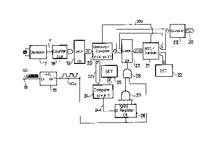
A frequency detector instructed in accordance with
the present invention comprises, as shown for example in
Fig. 3, a counter 18 for counting a reference clock F during
an N-divided period of a horizontal synchronizing signal HD
serving as a signal to be measured and an addi~g/subtracting
circuit 21 for adding or subtracting (only under the
condition described below) a first constant ~ to or from a
setting cycle y in response to a level difference between a
count value x of the counter 18 and the setting cycle y~ In
particular, when the difference between the count value x of
the counter 18 and the setting cycle y exceeds a second
constant ~, an approximate value of a period TH of the
horizontal synchronizing signal HD is obtained while
changing the setting cycle y by + ~ to produce an output
PATENT APPLICATION
value y + ~. ~his process is repeated as necessary to
enable detection of the period and therefore the frequency
fH of the horizontal synchronizin~ signal HD.
According to the present invention, as set forth
above, if the frequency of the reference clock F is taken as
fCK and the period of the horiæontal synchronizing signal HD
is taken as TH~ the count value x of the reference clock F
during the N-divided period o~ the horizontal synchronizing
signal HD is expressed as:
X = M-TH fCK .. . (1)
Until the difference between the count value x and the
setting cycle y becomes less than the second constant ~, the
first constant ~ is added to or subtracted from the setting
cycle y. Therefore, in case of an error -~ ~ as shown in
Fig. 4C, there is obtained from equation (1) the following
equation:
y ~ x = N TH fCK
Since x, N and fCK are already known, an approximate value
of the period T~ of the horizontal synchronizing signal HD
can be calculated from equation (2). Further, since the
frequenc~ fH of the horizontal synchronizing signal HD is
the reciprocal of the period TH, the frequency fH can be
obtained from the period TH.
If a pulse dropout occurs in the horizontal
synchronizing signal HD, the setting value y is not changed
50 lon~ as the difference between the count value x and the
setting value y is less than + ~. A stable detected value
of the frequency f~ is thus reliably obtained in spite of
possible dropouts of the signal to be detected.
-10--
~ 3 ~ 3 ~ ~ PAT~NT APPLICATION
A preferred embodiment of a frequency detector
constructed in accordance with the present invention will
now be described with reference to the drawings.
The block diagram forminq Fig. 3 shows in detail a
preferred embodiment of a frequency detector constructed in
accordance with the present invention. As that figure
shows, an input terminal 15 is supplied with the horizontal
synchronizing signal HD of frequency f~ and period TH. The
frequency fH of the horizontal synchronizing signal HD
generally falls within a range of lS kHæ to 130 kHz. The
input terminal 15 is connected to an input terminal IN of a
divide-by-N frequency divider 16, hereinafter referred to as
an N frequency divider. The N frequency divider 16 produces
at its output terminal OUT a signal HDN which results from
dividing the horizontal synchronizing signal HD by N. In
the preferred embodiment of the invention, N = 128.
An oscillator 17 produces a reference clock F
having a frequency fCK- The re~erence clock F is supplied
to a trigger terminal of a succeeding counter 18. The count
value of the counter 18 is supplied to an input terminal of
a latch circuit 19, and the N-divided signal HDN is supplied
to the clear terminal CLR of the counter 18 and the clock
terminal CK of the latch circuit 19. Accordingly/ a value x
held at the outpu~ terminal of the latch circuit 19
indicates the number of pulses of the reference clock F
counted during every N cycle of the horizontal synchronizing
,~' ` ,, '
,`, ~ ? : :
', ' ' ~
PATENT APPLICATION
~3~32~ 7217/3~258
signal HD. The value x is expressed by the following
equation:
x = N TH/(l/fcK) = N TH fCK
Thus, x is sometimes referred to hereinafter as a cycle
count value.
The cycle count value x is supplied to one input
terminal of a computing and comparing circuit 20, while the
computing and comparing circuit 20 receives at its other
i~put terminal a setting cycle y which homes-in on the value
of x in one or more iterations as will be explained in more
detail latex. The computing and comparing circuit 20, on
the basis of the cycle count value x and setting cycle y
received as inputs, calculates an error value z that is
defined as:
z = x - y ... (4)
and supplies the same as an error signal to an output signal
line 20b. At the same time, the circuit 20 supplies a
compared signal 20a corresponding to the positive or
negative pol rity of the error z to the adding/subtracting
circuit 21. The compared signal 20a is set at high level
"1l' when the error z, for example, is positive or zero,
while it is set a low level "0" when the error z is
negative.
The adding/subtracting circuit 21 ls supplied at
one of its input terminals with the setting cycle y and at
another of its input terminals with a constant ~ that is set
by a setting circuit 22. In general, the frequency fH of
;
3 13 2 ~ ~ PATENT APP~ICA~ION
7217/34258
the horizontal synchronizing signal HD is selected to be
about 20 kHz (period of 0.05 ms) so that, if To = 0.05 ms,
the constant a is selected so as to satisfy ~he following
equation:
~ = N~To fcKl5l2
The addinglsubtracting circuit 21 produces, when the
compared signal 20a is at high level "1", or an inequality
x - y > 0 is established, an output of y + , while it
_
produces, when the compared sisnal 20a is at low level "0",
or an inequality x - y < 0 is established, an output
y - ~. The output value y + a from the addiny/subtracting
circuit 21 is supplied to an input terminal of a latch
circuit 23, which latches to this value as the updated value
of y.
The error z, which is the output value of the
computing and comparing circuit 20, is supplied to one input
terminal of a comparing circuit 24, and the comparing
circuit 24 is supplied at its other input te~minal with an
output value ~ from a setting circuit 25. The comparing
circuit 24 supplies a compared signal 24a to a data terminal
D of an M-bit shift register 26. The compared signal 24a
goes to a high level "1" when ¦ z ¦ > ~ is establis~ed, while
it goes to a low level "0" when lz I < ~. In the preferred
embodiment of the invention, the value ~ is set so as to
satisfy the following equation:
~ = N To fCK/ ... l6)
Generally, the value ~ is selected to be such that the value
becomes smaller than 2 ~or even, as Fig. 4C shows, smaller
than ~.
-13-
.. .
~ 3 ~ 3 2 ~ ~ P TENT AP LICATION
In this embodiment, M of the M-bit shift register
26 i5 selected to be a plurality such as four (M = 4~, and
the four-bit output signals from the shift register 26 are
supplied to input terminals of a four-inp~t AND gate 27.
The output signal from the four-input AND gate 27 is
supplied to one input terminal of an AND gate 28, and the
N-divided signal HDN is supplied to the other input terminal
of the AND gate 28 and to the clock terminal CK of the M-bit
shift register 26. The output signal from the AND gate 28
is supplied to the cloc~ terminal CK of the latch circuit 23
50 that, if the N-divided signal HDN rises when the four-bit
output signal of the M-bit shift register 26 is at high
level "1" and the output of the AND gate 27 is therefore
also high, the setting cycle y, which is the output value of
the latch circuit 23, is changed to the output value y +
of the adding/subtracting circuit 21.
The latch circuit 23 acts to set the setting cycle
y, when the power switch is turned ON, at N T~ fCK by using
the cycle or period To where the frequency is 20 kHz.
Therefore, this value of y is referred to as the initial
setting cycle or period. Since the output of the M-bit
shift register 26 goes to a high level so long as the
compared signal 24a is at a high level, the setting cycle y
is adjusted to a value of y ~ ~ at the leading edge of the
N-divided signal HDN, and thus the setting cycle y
approaches the cycle count value x. When the compared
signal 24a finally goes to a low level "~", or the
-14-
,:
3 2 2 ~ PATENT APPLI CATI ON
~ 31 i 7217/34258
relationship
Izl = Ix - Yl ~ 7)
is established, the output signal from the four-input AND
gate 27 goes to a low level so that the setting cycle y as
the output value of the la~ch circuit 23 is not further
adjusted. Accordingly, since the setting cycle v is fixed
near the cycle count value x within the error + ~, from
equations (3~ and (6), there is obtained the following
inequality
I H CK Yl ~ N To fCK/256
From this it follows that the inequality
T ~ 256 < ~ < T~ + 256 ' ... t8)
is established. Since N and fCK are already known, the
cycle T~ of the horizontal synchronizing signal HD is
calculated from the value of cycle y within the error of
+ To/256.
This setting cycle y is supplied to a computing
circuit 29, and the computing circuit 29 computes a
detecting frequency fH' of the horizontal synchronizing
signal HD on the basis of the following equation:
f H ~ f C}C / Y
If ~ assumes the maximum error of the detecting
frequency fH', then, from equation (8~, ~f can be expressed
by the following equation:
_ 1 1 = fH f
TH - To/256 TH 1 - ~ (256 ft~) H
'--fH (fH/fQ)/256 ... ~lt))
The maximum error ~ when the frequency fH of the horizontal
synchronizing signal HD is fO (20 kHz) becomes about 0.1
-15-
`' ~ , , :
~,,
.. .... . . . .
. .:
, .
: ~ ~
~ ~ PATE;NT APPIIICATION
~ 22~ 7217/34258
kHz.
The operation of this embodiment of the invention
until the setting cycle ~ is stabilized in the freauency
detector is as follows: ~et it he assumed that the cycle or
period TH of the horizontal synchronizing signal HD is
longer than the cycle or period To~ that the horizontal
synchronizing signal HD and its N-divided counterpart signal
HDN are presented as shown in Figs. 4A and 4B, respectively,
and that all bits of the output from the M-bit shift
register 26 in Fig. 3 are set at a high level "1". The
hatched area in Fig. 4C is the area in which the error o
the cycle count value x lies within * ~.
At this time, the value of the setting cycle y
when the po~er switch is turned ON is set at y0
(= N To fCK)- At time tl at which the N-divided signal HD~
rises, since TH > To is established as indicated above, the
ine~uality x > y is established and the setting value y is
adjusted to y0 ~ ~ ~see Fig. 4C). Slmilarly, at times t~
and t3 where the N-divided signal HDN respectively rises,
the setting value y is adjusted to y + ~. In this case, the
setting value y which is changed at time t3 satisfiec
x - y < ~ so that the compared signal 24a of the comparing
circuit 24 in Fig. 3 goes to a low level. Accordingly, at
the next time t4 in which the N-divided signal HDN rises,
the value held in the latch circuit 23 in Fig. 3 is not
updated. As a result, as Fig. 4~ shows, the setting cycle y
is not adjusted. Further, if there is a pulse dropout A1 in
the horizontal synchroni~.ing signal HD as shown in Fig. 4A,
-16-
., ,. ~ , :
PATENT APPLICATION
~ 3~3,2~ 7217/3~258
the cycle count value x at time t5 at which the N-divided
signal HDN rises is changed to xl. In this case, however,
the relationship expressed by the inequality x - y< ~ is
satisfied so that the setting cycle y at time t~ at which
the N-divided signal HDN rises next is not changed at all.
If there is a large pulse dropout A2 in the
horizontal synchronizing signal HD (see Fig. 4A) before time
t6, the value of the cycle count value x is changed to x2,
satisfying x - Y ~ e. Thus, the compared signal 24a of the
comparing circuit 24 in Fig. 3 goes to a high level.
However, at times t4, t5 and t6, data of three bits at a low
level are stored in the M-bit shift register 26 so that at
time t7 at which the N-divided signal HDN rises next, the
output signal from the AND gate 28 shown in Fig. 3 stays at
a low level. Thus, again in this case, the setting cycle y
is not changed at all. Further, even if there is a large
pulse dropout A3 in the horizontal synchronizing signal HD
between times to t6 and t7 as shown in Fig. 4A a~d the cycle
count value x is changed to X3, the output from the AND gate
28 shown in Fig. 3 stays at a low level, thus inhibiting the
setting cycle y from being adjusted at time t8 at which the
N-divided signal HDN rises. Therefore, the detecting
frequency fH' calculated on the basis of the equation (9~ lS
stable even in the presence of dropouts.
In this embodiment, since the four-bit shit
register is used as the M-bit shift register 26 in Fig. 3 r
the value of the setting cycle y is not adjusted so long as
the condition expressed by the inequality I x - y I ~ ~does
-17-
.:
.
.. . ...
... .
:-.
: . : :. . , : : , :
~ PATEMT APPLICATION
` ~ 3 1 3 % 2 1 7217/34258
not occur four times consecutively at the leadinq edge of
the N-divided signal HDN. Accordingly, even if pulse
dropouts occur in the horizontal synchronizing signal HD in
succession, the detecting frequency does not fluctuate and
undesired switching, hunting or the like does not occur in
the succeeding circuitry.
Since the error between the cycle count value x
and the setting cycle y quickly settles within the constant
~, the setting cycle y is not varied at all regardless of
the fluctuation of the horizontal synchronizing signal HD
from a time base standpoint. Also, even when the frequency
of the horizontal synchronizing signal HD is increased, the
frequency can be detected with accuracy substantially the
same as that described above.
In addition to detecting the frequency of the
horizontal synchronizing signal of the incoming video signal
as described above, the frequency detector of the present
invention is effective in obtaining a stable frequency under
the circumstance that the frequency of a signal to be
measured fluctuates because of the occurrence of pulse
dropouts, time base errors or the like.
A frequency detector constructed in accordance
with the present invention as described above can detect the
frequency to be measured with high accuracy even if the
frequency of the signal may have any frequency within a wide
range. Also, the frequency detector of the present
invention can stably detect the frequency regardless of the
occurrence of pulse dropouts, time base variations or the
-18-
131 3 2 21 PA ENT APPLICATION
like in the si~nal to be measured.
The description set out above is of cours~
presented merely by way of example. While a single
preferred embodiment of the invention is described, it will
be apparent that many modifications and variations thereof
can be effected by one having ordinary sXill in the art
without departing from the spirit and scope of the novel
concepts of the invention. For example, the M-bit shift
register 26 is not limited to four outputs, and the values
of a and ~ can be adjusted in the discretion of a user of
the apparatus, as those skilled in the axt will readily
understand. The scope of the invention should therefore be
determined only by the appended claims.
--19--
: : ",