Note: Descriptions are shown in the official language in which they were submitted.
3L3~3~2~
20365-2928
APPARATUS FOR RECOVERING AN ALTERNATING
VARIABLE IN A CONTROLLED SEMICONDUCTOR
Specification
The lnvention relates to an apparatus for recovering an
alternating variable, especially of an alternating current, having
a direct current componen~, a controlled semiconductor
component having an electromagnetic ~ransducer for measurement
purposes.
When an alternating variable is transmitted by means of
an electromagnetic transducer, a steady-state direct current
component is not transmitted. The consequence is a null or zero-
point shift in the alternating variable emitted by the transducer
as compared with the input alternating variable. This problem is
particularly prevalent in measuring currents in controlled
semiconductor components. For instance, a direct component can
arise in the current course of a thyristor adjustor as a result of
unequal ignition angles for the individual thyristors. ~ince the
measured alternating variable is required for the control of the
; thyristors, it is particularly importan~ to obtain an
unadulterated value.
With special precautions, devices previously used for
this purpose were capable of transmitting a direct current
component. These devices included transducers with a special
supplementary winding, for instance, by way of which a
premagnetization of the transducer core is effected for
counteracting the magnetization resulting from the direct
component. Such ~ransducers are expensive. Moreover, they
',, ~ " - . .
~ .
.. : : ,.
~313~2~
20365-2928
require additional regulating devices for the premagnetization.
It is accordingly an object of the invention to provide
an apparatus for recovering an alternating variable in a
controlled semiconductor, which overcomes the hereinaiore-
mentioned disadvantages of the heretofore-known devices of this
general type and with which the electrical alternating variable
having a direct current or DC component can be simulated in a
simple manner for measurement, regulating and control functions,
in a controlled semiconductor component.
With the foregoing and other objects in vie~ there is
provided, in accordance with the invention, an apparatus for
recovering an alternating variable, especially an alternating
current, having a direct current component of a controlled
semiconductor component, comprising an electromagnetic transducer
for measurement having a secondary winding, a sample and hold
element having a triggex input, an output and another input
connected to the secondary winding of the transducer, a control
system for the semiconductor component connected to the triyger
input for feeding trigger pulses from the control system to the
trigger input at respective control times of the semiconduckor
component, and a comparator having a ~irst input connected to the
output of ~he sample and hold element for receiving an output
signal proportional to the direct current component, a second
input connected to the secondary winding of the transducer and an
output supplying the recovered alternating variable.
In this way, a recovery of the required electrical
alternating variable, together with its direct component~ is
'
, ': .
~31322~
20365-2928
attained with simple means. Conventional economical transducers,
such as typical protective transducers, can be used for detectiny
the measured value. ~ue to their small size, these transducers
additionally contrihute to a substantial reduc~ion in the amount
of space required, as compared with the conventional structure
having a supplementary winding. With the apparatus according to
the instant application, it i.s possible to detect very small
direct current components. Only the DC components that are
steady-state and are not transmitted by ~he transducer are taken
into account in this process.
In accordance with another feature of the invention, the
comparator is a subtractor, the first input o~ the comparator is
an inverting input, and the second input of the comparator is a
non-inverting input. In this way, the recovered alternating
variable (DC and AC component~ also correspond in its phase to the
originating alternating variable.
This advantage is also present if in ac~ordance with a
further feature of the invention, there is provided an inverter
element disposed between the sample and hold element and the
comparator or at the other input o~ the co~parator, the comparator
being in the form of an analog adder.
In accordance with an added feature of the invention,
the inverter element and/or the comparator is an amplifier. In
this way, an adaptation of the ratios o~ the levels between the
transducer and the elements connected to the output side thereof
can thus be obtained, which makes it possible to detect even ~uite
small DC components.
;~ 3
~. ~
`
~31~2~
20365~2928
In accordance with an additional feature of the
invention, there is prcvided a stop and low-pass fllter array
connected to the output of the comparator, and a measuriny output
connected to the stop and low-pass filter for supplyiny the
recovered alternating variable. In this way the entire DC
component contained in the al~ernating variable is present at the
measurement output and available for further purposes. This
measuxement signal can advantageously be used through the control
system, to regulate out the undesired direct current component.
In accordance with yet another feature o~ the invention,
the semiconductor component includes at least one thyristor.
In accordance with yet a further feature of the
invention, the semiconductor component is a component of a
thyristor final control element.
In a~cordance with a concomitant feature of the
; invention, there is provided a measuring instrument connected to
the measuring output for indicatiny a current.
Other fea~ures which are considered as characteristic
for the invention are set forth in the appended claims.
Although the invention is illustrated and described
herein as embodied in an apparatus for recovering an alternatiny
variable of a controlled semiconductor, it is nevertheiless not
intended to be limited to the details shown, since various
modifications and structural changes may be made therein without
departing from the spirit of the invention and within the scope
and range of equivalents of the claims.
i 4
. "
'
~31322~
203~5-292~
The construction and method of operation of the
invention, however, together with additional objects and
advantages thereof will be best understood from the following
description of specific embodiments when read in ~onnection with
the accompanying drawings.
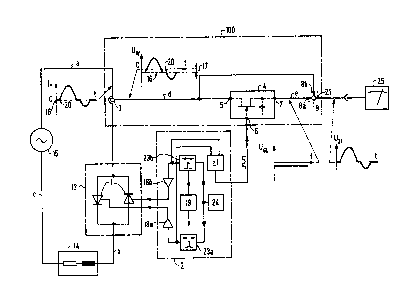
Fig. 1 is a schematic circuit diagram of a first
apparatus for recovering the alternating current at a thyristor
final control element; and
Fig. 2 is a diagram similar to Fig. 1 of a second such
apparatus.
Re~erring now to the ~igures of the drawing in detail
and first, particularly, to Fig. 1 thereof, there is seen an
appaxatus 100 for recovering an alternating variable of a
controlled semiconductor component, in particular a thyristor.
The conkrolled semiconductor component or thyristor is a component
of a thyristor final control element 13, which forms a current
circuit with lines a, b, c, a load 14 and a voltage source 15. A
current IT flows ~hrough the final control element 13 as shown.
It should be noted that the two half-waves are of different sizes
because of unequal iynition angles, and the current source there-
fore has a DC component. The component should be a steady-state
component. Semiconductor components 1 of the final control
element 13 receive their control pulses from a control system 2.
The control system 2 includes a pulse generator 24 providing
output pulses which are transmitted to the controlled semiconduc-
tors 1 through angle control means 23a, 23h and adaptation stages
18a, 18b. The current IT is de~ec~ed by a transducer 3.
~-'f~ 5
~313~
A voltage Uw at the secondary side of a transducer 3 is
transmitted to a line d as shown by means of the transmis-
sion properties of the transducer 3. It can be seen that
the DC component is suppressed by the transducer 3. The
voltage/time areas of the positive and negative half-waves
belonging to one another are of equal size. An original
zero line 16 of the course of the current IT is shifted
downward by an amount 17 equal to the DC component. The
voltage Uw is fed through the line d to one input 5 of a
sample and hold element 4, having a trigger input 6 which is
coupled to the control system 2.
The sample and hold element 4 receives trigger pulses from
the control system 2 at each control time 20 of the semicon-
ductor components 1. In this way it is ensured that the
voltage Uw is sampled at each of the control times 20 of the
semiconductor components l and this value is emi~ted at an
output 7 of the sample and hold element 4 until such time as
a subsequent trigger pulse follows. At the control time 20,
the current IT of the semiconductor components 1 is zero.
If the value Uw is observed at these times 20 9 then the
amount 17 is precisely the proportion of ~he DC component.
An output signal UGL of the sample and hold element 4 on a
line e is accordingly proportional ~o the DC component.
The output 7 is connected to a first input 8a of a
comparator 9, having a second input 8b which is connected to
t e secondary winding of the transducer 3. It is
-- ~3~322~
20365-2928
advantageous for the comparator g to be ~onstructed as a
subtractor, wi~h the first input 8a constructed as an inverting
input and the second input 8b as a non-inverting input. This
means that the DC component UGL is subtracted from the alternating
variable Uw. A correct-phase replica UIT of the original
alternating variable IT is then present at an output 21 of the
comparator 9. The signal UIT is then used for furthar measurement
purposes. For instance, it can be transmitted to temperature
monitors, monitoriny and regulating devices r or to a measurin~
instrument 25 ~hat displays the current value as shown.
Fig. 2 shows another exemplary embodiment in which the
comparatox 9 is constructed as an analog adder. In order to
ensure that the direct current component will be added to the
transducer signal with the correct polarLty, an inverter element
10 is disposed between the sample and hold element 4 and the
comparator 9. Alternatively, an inverter element lOa may be
disposed at the input o~ the sample and hold element 4. The
inverter element 10 or lOa and/or the comparator 9 are preferably
constructed as amplifiers, in order to attain optimal adaptation
of the various elements to one another.
A filter 12, constructed as a stop or rejection and low-
pass filter, is disposed between the output 21 of the comparator 9
and a ~easuring output 22. The filter 12 ensures that all
.i,i
, ~ . . ..
'- .,
~ . - , . ,
" ~ :
~` ~' ' ,' ' ,
~3~3~2~
of the alternating current components of the voltage UIT are
eliminated, so that a voltage UF that is proportional to the
total DC component contained in the current IT, is present
at the measuring output 22. This vol~age can, for instance,
be carried by a line f to a control unit 19 of the control
system 2 9 in order to a~tain an undesired DC ~omponent in
the load current circuit by correcting the con~rol instants.
This is particularly important if the load 14 is inductive
and an undesired premagnetization takes place. The voltage
UF serves as a standard for the premagnetization. Alterna-
tively, the voltage may also be supplied to monitoring
devices or, as shown~ to a measuring instrument 25a.
A substantial advantage of the apparatus 100 or lOOa is that
only ~he DC component that is not transmitted by ~he trans-
ducer 3 is detected by the sample an~ hold element 4. In
other words, components that arise dynamically for brief
periods, and can be transmitted to the transducer 3, are not
detected by the sample and hold element 4. In contrast to
the signal Uw, ~hey exhibit no temporal shift in the alter-
nating variable to the secondary side of the transducer 3.
Accordingly, dynamic components are especially taken into
account, and can optionally be further treated in ~he filter
array 12.