Note: Descriptions are shown in the official language in which they were submitted.
8~ ~'. AT9~87-031
1313275
Description
PARALLEL PROCESSOR INSTRUCTION DISPATCH APPARATUS
WITH INTERRUPT HANDLER
. .
Technical Field
This invention relates to data processing and
- more specifically to interrupt processing in a paral-
lel data processing system.
Background Art
Traditional processors execute instructions in a
serial fashion, i.e., one instruction at a time. In
order to increase the operating efficiency and ~speed
of execution of data processing systems, parallel
processing has been implemented. Parallel processing
provides for the concurrent e~ecution of instructions.
However, it is desirable to concurrently execute the
instructions in such a manner that they will appear to
be serially executed. The use of multiple execution
units in a data processing system provide execution of
instructions concurrently when several instructions
- can be distributed or dispatched to individual execu-
tion units for simultaneous execution during a time
period or cycle. An instruction dispatching apparatus
is required to determine which instructions should be
dispatched to which execution units. An example of
one such dispatching apparatus is disclosed in the IBM
Technical Disclosure Bulletin, Volume 29, No. 1, June,
1986~ entitled "Branch-Processing Tnstruction Cache",
pages 357-359. This disclosùre illustrates a mecha-
nism for fetching instructions and includes the
capability to process branch instructions while other
instructions are being fetched.
$~
, ,,, ,~ . . - , . . . , ~
~ D AT9-87-031
1 3 1 3275
I
One problem that arises in the parallel concur-
rent processing of instructions is the handling of an
instruction generated interrupt in a manner that will
maintain the appearance of serial instruction execu-
tion.
It is the object of the present invention to
provide a mechanism for handling interrupts while
providing for the concurrent execution o~ instruc-
tions.
Disclosure of the Invention
In accordance with the present invention, a data
processing system for executing a sequence of instruc-
tions is provided. The data processing system in-
cludes several processors, ea~h for executing instruc-
tions. Also included is a dispatching apparatus for
dispatching each of the instructions to one of the
processors~ A control apparatus is included for
directing the concurrent execution of the dispatched
instructions in the processors irrespective of the
locations of the instructions in the sequence. The
control apparatus includes the capahility to receive
an instruction interrupt signal. Upon receiving the
instruction interrupt signal, the control apparatus
determines which ins~ruction execution generated the
instruction interrupt. The control apparatus includes
the capability to reset the processors and the dis-
patching apparatus to the state that existed when the
instruction that ~enerated the instruction interrupt
signal was ~irst executed in order to re-execute the
instruction that caused the interrupt.
In the pre~erred embodiment, the control appara-
, tus includes the capability to maintain a history o~which instructions were dispatched to which proces-
sors. The control apparatus ~urther maintains a
.. ~ . . .. ...
.
AT9-87-031
13~3275
record of the contents of selected registers. Upon
the occurrence of an interrupt signal, the control
apparatus is able to determine the state of these
registers and the state of the processors that existed
at the time the instruction was first executed. The
control apparatus then reinitializes all of the
processors with the information that has been stored
to place the processors and the instruction dispatch-
ing apparatus into the state that existed when the
instruction that caused the interrupt was first
executed.
Brief Descxi~tion of the Drawing
The novel features believed characteristic of the
invention are set forth in the appended claims. The
invention itself, however, as well as the other
features and advantages thereof, will be best under-
stood by reference to the detailed description which
follows, read in conjunction with the accompanying
drawings, wherein:
Figure 1 is a hlock diagram of a parallel data
processing system;
Figure 2 is a block diagram illustrating a
portion of the data processing system of Figure l;
Figure 3 is a ~lock diagram illustrating portions
- of the program counter stack and the branch execution
unit;
Figure 4 is a diagram illustrating the contents
of the program counter stack entry;
Figure 5 is an illustration of the instruction
registers and stack register contents during cycle
zero;
Figure 6 is an illustration of the contents of
the instruction registers and stack xegisters during
cycle l;
,, , , ~, , ~ . . ~ ,.. . . . .. .. .. .
AT9-87-Q31
1 3 1 3275
Figure 7 is an illustration of the contents of
the instruction registers and stack registers during
cycle 2;
Figure 8 is an illustration of the contents of
the instruction registers and stack registers during
cycle 3;
Figure 9 is an illustration of the contents of
the instruction registers and stack registers during
cycle 4;
Figure 10 is an illustration of the contents of
the instruction registers and stack registers during
cycle 5;
Figure 11 is an illustration of the contents of
the instruction registers and stack registers during
cycle 6;
Figure 12 is a flow chart illustrating the
simultaneous execution of the stack addition ~unction
and the stack removal function;
Figure 13 is a flo~J chart illustrating the stack
addition function; and
Figure 14 is a flow chart illustrating the stack
removal function.
Best Mode for Carrying Out the Invention
This invention ~rovides a mechanism for ~he
: parallel and concurrent execution of several instruc-
; tions while permitting interrupts to be processed in
such a manner that the instruction execution will
. appear to be serial.
; 30 Figure 1 is a block diagram illustrating a data
processing unit including a memory 10 connected to a
memory controller 12 and instruction buffer 14.
, Connected to the instruction buffer 14 is a program
counter stack and instruction dispatch logic 16.
Several execution units 18a through 18d are in turn
. .
.. . . .... .. ...
.~ ~
AT9-37-031
1313275
connected to the program counter stack and instruction
dispatch logic 16. The execution units 18a through
18d are connected to an information bus 20 which
provides for the distribution of informa~ion through-
out the data processing systemO
Figure 2 is a block diagram illustrating the
instruction buffers 14 connected via bus lines 1 to
instruction issue logic 17. The instruction issue
logic 17 is further connected via buses 2 and 3 to the
program control stack 15. The instruction issue logic
17 and the program counter stack 15 make up the block
16 of Figure 1. Also illustrated are instructions
units 18a, 18b, 18c and 18d. It should be apparent to
those skilled in the art that the number of execution
units included mav vary in accordance with the number
; of instructions to be concurrently executed. In the
prefexred embodiment, e~ecution unit 18a executes
branch instructions. Execution unit l~b executes
fixed point arithmetic instructions. R~ecution unit
18c executes floating point arithmetic instructions.
In this preferred embodiment, execution units 18a
through lac are the only ones that are functiona].
The instruction buffer 14 stores a large group of
instructions that are received from the memory 10
(Figure 1). The ins-truction issue logic 17 loads
instructions from the instruction buffer 14 into the
available execution units 18a through 18d. In the
preferred embodiment, the instruction issue logic 17
can load four instructions simultaneously to the
execution units 18a - 18d. The instruction issue
logic 17 further determines which instruction goes to
- which execution unit and if the execution unit is able
to take an instruction. Furthermore, the instruction
issue logic 17 provides an input over lines 2 to the
program counter stack. This input includes the record
. .
. . ..
AT9-87-031
1 31 3275
of the instructions dispatched. The program stack
counter 15 provides a signal over line 3 to the
instruction issue logic to stop the dispatching of
instructions. This signal occurs when either an
interrupt has been generated or when the stacks in the
program counter 15 are full. The instructions from
the instruction issue logic 17 are provided to the
; appropriate execution units. The branch execution
unit 18a provides information to the program counter
stack such as addresses and the values of certain
registers over line 7. The fixed point arithmetic
instruction execution unit 18b provides signals over
line 9 indicating the completion of instructions or
the occurrence of an instruction interrupt signal.
The fixed point arithmetic instruction execution unit
18b further provides and receives signals from the
floating point arithmetic instruction execution unit
18c over line 11. These signals over line 11 provide
for svnchronization between the floating point and
fixed point execution units for the execution of
floating point load and store instructions. In this
embodiment, the fixed point execution unit 18b com-
pletes address calculations floating point load and
store instructions. The fixed point execution unit 18b
then sends these addresses to memory. For store
instructions, the fixed point unit 18b must know when
the floating point unit 18c has completed execution of
the instruction so that the fixed point unit 18b will
know when data is ready to be stored and therefore,
when the address is ready to be transmitted. Further-
more, the fixed point unit 18b signals the occurrence
of interrupts to the floatin~ point unit 18c so that
, it will disregard the current floating point unlt
instruction.
AT9-87-031
1313275
Figure 3 illustrates, in a more detailed fashion,
the intercommunication between the branch unit 18a and
the program counter stack 16. In Fiaure 3, the branch
unit 18a is shown to contain the count register 22,
the link register 24, the condition register 26, and
the interrupt address register 28. The count register
22 maintains a count for the execution of loop in-
structions in the branch execution unit 18a. The link
register 24 maintains the address for link operations
such as the return from a subroutine call. The
condition register 26 maintains the condition codes
that result from comparison operations. The interrupt
address register 28 receives the ad~ress of an in-
struction that ha~ generated an interrupt. The count
register 22 is connected b~ lines 40 and 42 to the
count register backup stack 30 in the program counter
stack 16. Likewise, the link register 24 is connected
to the link register backup stack 32 by lines 44 and
46. Also, the condition register 26 is connected via
lines 48 and 50 to the condition register backup stack
34. The interrupt address register 28 is connected
via line 70 to an adder 75. The adder 75 produces the
interrupt address for the interrupt register 28 via
line 71. The contents of these registers 22, 24, 26
and 28 control the-state of the execution of the
branch execution unit 18a.
Since the occurrence of an interrupt will stop
the execution of execution units 18b and 18c, the
re-execution of an instruction by the branch execution
unit 18a will reinitialize the execution of an in~
struction sequence at the instruction that generated
the interrupt.
When the instruction issue logic 17 (Figure
issues four or less instructions in a cycle, the
program counter storage entry storage table 36 is
.. ~
,
o~ r
AT9-87-031
1313275
updated. The base address is pro~ided on line 56.
The mask and two fields are provided from line 54 from
the program counter stack control 38. The program
counter stack control 38 receives this information via
line 63 from the instruction issue logic 17. Addi-
tionally, the program counter stack control 38 updates
stack pointers 39 which contain head pointers and tail
pointers for the three backup stacks 30, 32 and 34,
and executes the stack removal and stack addition
functions performed by the stack addition logic 64 and
stack removal logic 66.
The program counter stack control 38 regulates
the operation of the backup stacks 30, 32, and 34 by
line 52. Furthermore, this control 38 provides the
: 15 stop dispatch signals to the instruction issue logic
17 on line 62 and recei~res the instruction complete
and interrupt signals from the fi~ed point execution
unit 18b on line 60 as previously discussed.
The program counter stack entry storage 36 pro-
vides the address of the interrupting instruction on
line 70 to the interrupt address re~ister 28.
Figure 4 is an illustration of the contents of
the pro~ram counter stack entry storage 36 (Figure 3).
A single entry 80 is listed that includes the base
instruction address field 82, the 4 bit mask field 84,
the instruction 1 field 86 ~nd the instruction 2 field
88. Field 82 is the address of the base instruction
for the 4 instruction sequence that has been dis-
. patched in the cycle by the instruction issue logic 17
IFigure 2). The mask field 84 indicates the position
of any interrupt causing instructions in this 4
instruction group. In the present embodiment, onl~
, two instructions can cause interrupts in a 4 instruc~
tion group. Therefore, there are only two instruction
fields 86 and 88 provided to record these
. .
AT~-87-031
1 3 1 3275
instructions. The first instruction ~ield 86 includes
sub-fields 90, 92, and 94. Field 94 indicates whether
the link register 24 has been changed. Field 92
indicates whether the count register 22 has been
changed. Field 94 indicates whether the condition
register 26 has been changed. In the preferred
embodiment, field 90 and 92 contain 1 bit each. Field
94 contains 3 bits indicating the three separate
portions of the condition register 26. Field 88 also
contains fields similar to field 86 and are illustrat-
ed as fields 96, g7 and 98 that correspond to fields
90, 92 and 94 previously discussed.
The operation of this invention is best under-
stood by an example illustration. Table 1 lists
twelve instructions that are to be dispatched for
e~ecution by the execution units. These instructions
are divided up into three groups of four instructions
each. For this example, the address of the first
instruction is 1. Group I consisting of instructions
1 through 4 are dispatched in cycle 1.
Figure 5 illustrates the contents of the program
counter stac]c entry storage 36 consisting of entry
positions 100, 102 and 104; the count register backup
stack 30, consisting of entries 30a, 30b and 30c; the
link register backup-stack 32, consisting of entries
32a, 32b and 32c; and the condition register backup
stack 34, consisting of entries 34a, 34b and 34c.
Additionally, the initial contents of the count
register 22, the link register 24 and the condition
register 26 are illustrated as 50, 60 and 70 respec-
tively. The actual value of these contents is arbi-
trary and is merely included to provide the reader
, with a trace the entries through this example.
Referring to Figure 6, during cycle 1, instruc-
tions 1 through 4 are dispatched. Since a load
,
.. r AT9-87-()31
1 3 1 3275
instruction ~instruction 1) was dispatched, one entry
will be added to the program counter stack entry
storage 36. In this embodiment, only load and store
instructions may generate interrupts. The base
address of "1" is stored. The mask value is 1000
denoting that the first instruction is the location of
the instruction that might cause an interrupt. If two
instructions were included in the four instruction
group, 2 bits of the mask field would be set to l~
The location of the bits denotes the location of the
interrupt causing instructions in the 4 instruction
se~uence. Therefore, the mask bit positions can be
used as offsets to the base address to provide the
actual addresses of the interrupt causing instruc-
tions. The contents of field 1 are set if the countregister 22, the link register 24, and the condition
register 26 contents are changed during the execution
of this four instruction sequence~ In this example,
the branch instruction sets the count register 22 and
link register 24. The LCR (logic on condition regis-
ter) instruction sets the contents of the condition
register 26. The previous contents of these registers
are stored as shown.
Figure 7 illustrates the status after cycle 2.
In cycle 2, instructlons 5 through 8 (group II of
Table 1~ are dispatched. Since group II is the exact
same set of instructions as group I, the same actions
occur to update the backup stacks respectively. ~lso,
the execution of instructions 7 and 8 update the count
register 22, the link register 2~ and the condition
register 26 as sho~m. The backup registers 30, 32 and
3~ store the previous contents of the count register
, 22, the link register 24 and the condition register
26. Each cycle an interrupt causing instruction is
dispatched a record of the dispatch c~cle is ~Jritten
. .
AT9-87-031
1313275
in to the program counter stack entry storage 36. I~
subsequent instructions cause the link register 24,
the count register 22, or the condition register 26 to
be updat~d, the old values of these registers are
stored in the appropriate backup stacks and the
respective tail pointers are incremented. There is a
head and tail pointer for each backup stack. These
pointers operate the three backup register locations
as a circular queue. Therefore, each time an entry is
made, the tail ~ointer is incremented. Each time an
entry is removed, the head pointer is incremented.
Figure 8 illustrates the contents of the registers at
the end of cycle 3 when the group III instructions
have been dispatched. For this example r during cycle
~ 15 3, the fixed point unit 18b executes instruction 1.
; For thls example, instruction 1 did not cause an
interrupt. Since only one interrupt causing instruc-
tion was dispatched ~uring this cycle (cycle 1), the
entire entry 100 may he removed. Using informatlon in
field 1, the backup register entries 30a, 32a and 3~a
are also removed. Thls is accomplished by increment-
ing the head pointer as previouslv discussed. Since
the group III instructions are similar to groups I and
II, the program counter stack storage entry 104 is as
shown. Likewise, the count register 22, the link
register 24 and condition register 26 are provided
with values 57, 67 and 77 respectively. The previous
values of these registers are stored in the appropri-
ate entries in their backup stacks 30, 32 and 34 a5
shown.
Figure 9 illustrates the contents of these
registers at the end of cycle 4. For this example, in
cycle 4 instruction ~ was executed by the fixed point
unit 18b. Since it is not a load or store instruc~
tion, it cannot cause an interrupt. Therefore, no
AT9-87-031
1313275
entries need to be removed from the program counter
stack entr-~ storage 36.
Figure 10 illustrates the contents of the regis-
ter at the end of cycle 5. During cycle 5, the fixed
point execution unit 18b has executed instruction 5.
For this example, this instruction has caused an
interrupt. In this case, the offset mask bits (lO00)
are combined with the base address (5) to determine
the position of the instruction that caused the
interrupt. In this example, the address is 5.
Additionally, since the field 1 tag bits were set for
the count register 22, the link register 24 and the
co~dition register 26, the backup values for these
registers are provided to these registers. These
15 values are stored in entries 30b, 32b and 34b respec~
tively. The address of the interrupting instruction
is provided to the branch execution unit 18a. Like~
wise, the backup register contents are provided to
their respective registers. The program counter stack
~0 entry storage 36 and backup stacks 30, 32 and 34 are
then purged of all information since this stored
informatlon is no longer relevant and the system is
being reinitialized to the state when the instruction
at location 5 was executed.
Figure 11 illustrates the register contents at
the end of cycle 6 when the condition register 22, the
link register 24 and the condition register 26 have
been updated. At the end of cycle 6, the system has
been reinitialized and is ready to start again the
execution of the instruction sequence starting at
instruction 5.
In this embodiment, if a single program counter
stack entry contains two instructions that might
generate interrupts, the interrupts are received on a
first-in, first-out basis. In other words, when an
AT9-87-031
13~3275
13
interrupt occurs, the oldest instruction that might
generate an interrupt is assumed to have generated
this interrupt. However, it should be apparent that
in other systems the oldest instruction is not neces-
sarily the instruction that causes the interrupt. Thesystem could then determine the instruction that
caused the interrupt by a tag that would be provided
by the occurrence of the interrupt.
Therefore, in Figure 11, the registers appear as
if only instructions l through 4 have been executed.
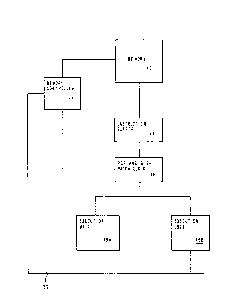
Figure 12 illustrates a state diagram depicting
the concurrent execution of the stack addition func-
tion in logic 64 (state 122) and the execution of the
stack removal function 124 in the stack removal logic
66. These functions 122 and 124 are executed during
each cycle as depicted by states 120 and 126.
Figure 13 is a flow chart illustrating the stack
addition function. At the beginning of the cycle, the
stack addition logic 64 beyins at step 200 and pro-
ceeds to step 202 to determine if a load or storeinstruction was dispatched. ~f so, the logic proceeds
to step 204 to store the base address and set the tag
offset bits of the program counter stack entry storage
36. If a load and store instruction was not dis-
patched or, after the base address and offset bitshave been stored, the logic proceeds to step 206 to
determine-if any branch or LCR instructions were
dispatched before a load or store instruction. If so,
the tag bits of the previous program counter stack
entry is updated and the old values of the count, link
and condition registers are stored on the backup
stacks. The program then proceeds to step 216.
, Returning to step 206, if no branch or ~CR instruc-
tions were dispatched before a load or store instruc-
tion, the lo~ic proceeds to step 210 to determine if
. , ,~ . .
AT9-87-031
1 3 1 3275
14
anv branch or LCR instructions were dispatched after a
load or store instruction~ If so, the logic proceeds
to step 21?. to set the tag bits of the present program
counter storage entry and to store the old values on
the backup stacks. Then in step 216, the backup stack
pointers 39 are incremented. Returning to step 210,
if no hranch or LCR instructions were dispatched after
a load or store instruction, the logic proceeds to
step 214 to set the tag bits of the present program
counter stack entry to zero. Then, in step 218, the
poirlter to the program counter stack entry is incre-
mented if a load or store instruction was dispatched.
Then in step 220, the logic determines if the program
counter stack entry storage is full. If so, a latch
is set in step 222 to send the stop dispatch signal to
the instruction issue logic 17. In step 224, the
logic 64 waits until tne next cycle has occurred when
- it returns to step 200.
~igure 1~ is a flow chart illustrating the stack
removal procedure performed by logic 66. Upon the
beginning of a cycle, the logic 66 moves from step 300
to step 30' to determine if a load or store instruc-
tion has been executed by the fixed point execution
unit. If not, the logic proceeds to step 310. If so,
the logic proceeds to step 304 to determine if all
load and store instructions in the program counter
stack entr~y storage were executed. If not, the
program proceeds to step 306 to wait until the next
cycle. If all of the load and store instructions for
the entry were executed, the logic proceeds to step
308 to remove the entry and use the status bits to
remove the backup stack entries and to decrement all
of the pointers. Upon the completion of step 308, the
logic proceeds to step 306 to wait ~or the next cycle.
~ q`
AT9-87-031
1 31 3275
Returning to step 310, the logic determines if a
load or store instruction caused an in~errupt. If
not, the logic proceeds to step 306. If an interrupt
has occurred, the logic proceeds to step 312 to
reconstruct the address of the load and store instruc-
tion from the base address and tag bits in the proqram
counter stack entr~. Then, in step 314~ the old
values of the link 24, count 22 and condition regis-
ters 26 are stored if appropriate. In step 316, the
contents of the program counter stack entry storage 36
and the respective backup registers are purged since
these values would no longer be relevant. The logic
66 then proceeds to step 306 to wait for the next
cycl~.
While the invention has been described with
reference to the illustrated embodiment, this descrip
tion is not intended to be construed in a limiting
sense. Various modifications of the illustrated
embodiment as well as other embodiments of the inven-
tion will become apparent to those persons skilled in
the art upon reference to this description. It is,
therefore, contemplated that these appended claims
will cover any such modifications or embodiments as
fall within the true scope of this invention.
-
` 35