Note: Descriptions are shown in the official language in which they were submitted.
13~3343
METAL ORGANIC VAPOR PHASE EPITAXIAL
1 GROWTH OF GROUP III-V SEMICONDUCTOR MATERIALS
DESCRIPTION
This invention relates generally to epitaxial
growth, and more particularly, to epitaxial growth of Group
III-V semiconductor materials. The technique employed is
metal organic vapor phase epitaxy (MOVPE). The MOVPE
technique involves introducing vapors of the reactants and/or
precursors into a reaction vessel wherein a chemical reaction
occurs to provide the epitaxial Group III-V material. Group
III-V compound semiconductors have applications, for example,
in light-emitting diodes, field effect transistors and
lasers.
PRIOR ART
The growth of epitaxial material of high electrical
and physical quality has been achieved in a variety of growth
techniques. The metal-organic vapor phase technique is one
of the most versatile and commercially desirable of the
techniques. The growth by MOVPE is, in general, a conformal
process.
In conventional MOVPE techniques for the epitaxial
growth of Group III-V materials, the Group III or the Group
III and Gxoup V metals are provided by metal-alkyl reactants
in vapor form. Since these metal-alkyl reactants decompose
at low temperatures into carbides and metal-alkyl polymers,
the MOVPE techni,que is typically undertaken in a system
wherein only the substrate is heated and the react~r walls
are cold to prevent the predeposition of the decomposed
Yo988-0l7 r~
-2- 13~3~43
reactants onto the reactor walls. The substrate is
selectively heated typically by an external rf induction coil
that couples energy through the reactor wall to the susceptor
which in turn heats the wafers, or by an external radiant
heater in direct contact with the reactor wall. The reactor
tube is conventionally made of quartz which is transparent to
the radiant heating and rf induction thereby remaining cool.
This typical MOVPE cold-wall reactor is limited in
the number of substrates and in total substrate area where
useful deposition can occur. This limited area of useful
deposition is attributed to complicated chemistry in addition
to complex, geometry dependent, fluid flow in these cold wall
systems which are operated in the near atmospheric pressure
regime (10-760 torr). Uniform growth is found only over a
limited area due to the mass transport limited nature of the
growth process at these conventional pressures. The use of
lower reactor pressures using the conventional MOVPE growth
chemistries of trimethyl gallium, trimethyl aluminum and
their analogues in the In based systems, result in the high
incorporation of carbon leading to undesirable materials
properties. The conventional precursors used in the MOVPE
process use three similar or identical saturated hydrocarbon
ligands, such as triethyl gallium, Ga~C2H5)3, Diethylmethyl
In, (C2H5)2InCH3, and so on. These precursors decompose at
low temperatures requiring a cold wall system in order to
insure their transport to the growth area without a
pre-reaction and decomposition on the inadvertently heated
reactor walls.
A method for vapor epitaxial deposition of Group
III-V compounds utilizing Group III organometallic compounds,
YO988-017
~3~ ~313343
1 such as triethylgallium and trimethylaluminum, in the
presence of gaseous halogen or hydrogen halides is disclosed
in U.S. Patent No. 4,147,571. The system has application in
cold-wall and hot-wall systems.
The use of diethylgalliumchloride and arsine for
epitaxial growth in a cold wall system at atmospheric
pressure was reported by K. Kindkete, W. Sack and J.J. Nick
in J. Electrochem. Soc. 117 ~Oct 1970) and Y. Nakayama, S.
Ohkawa, H. Hashimoto and H. Ishikawa in J. Electrochem. Soc.
123, 1227 (1976).
MOVPE growth on patterned substrates where part of
the free surface of the semiconductor is covered by masking
material, e.g. SiO2,SiNX, etc., results in a deposition of
material over the entire surface. The material deposited on
the mask is poly-crystalline (S.H. Jones and K.M. Lau, J.
Electrochem. Soc. 134, (lg87)3149) while the material
deposited on the substrate through openings in the mask is
single crystal. In order to achieve no deposition on the
masking material, as opposed to poly-crystalline deposition,
workers have to go to high growth temperatures, lower reactor
pressures, and low growth rates (H. Heinecke, A. Brauers, F.
Grafahrend, C. Plass, N. Putz, K. Werner, M. Weyers, H. Luth,
and P. Balk, J. Crystal Growth, 77, (1987)303). In these
latter studies, low supersaturation must be maintained in the
growth ambient to prevent the nucleation of GaAs on the mask.
In all cases complicated edge morphologies arise at the
boundary of the mask. This is attributed to the diffusion of
growth species from the mask surface to the edge of the
3 growing film.
YO988-017
~4~ ~313~43
The lack of selectivity in conventional MOVPE
arises from the choice of chemical precursor. Metal sources
such as triethyl gallium, trimethyl gallium and trimethyl
aluminum, all decompose readily to yield metallic deposits.
In order to get selective growth the evaporatiOn of the
metallic deposit must take place before sufficient metal is
deposited to nucleate a poly-crystalline deposit. This means
providing a low supersaturation in the growth ambient such
that the driving force for growth is small. This is
1 accomplished in conventional MOVPE by low growth rates, high
growth temperatures and low growth pressures.
Summarv of the Invention
The present invention is directed to a method for
growing Group III-V epitaxial layers in a hot wall system,
wherein the precursors for providing the Group III metal
contain a Group III metal, an organic ligand and an inorganic
ligand. The precursor is of the form:
2-y l+y
wherein
M is a Group III metal atom;
R is alkyl or halo-substituted alkyl;
X is halogen; and
y is O or 1.
In accordance with the method of the invention, a
3 substrate of a material suitable for epitaxial growth is
positioned in a hot wall reactor. A gaseous mixture is
introduced into the chamber that includes at least one
YO988-017
13133a~3
organometallic halide compound of a Group III metal and at
least one compound of a Group V element under conditions of
suitable temperature and pressure to deposit on the substrate
an epitaxial layer of a III-V compound.
At low temperatures compared to those required for
epitaxial growth, the R substituents fissure from the
precursor resulting in a transition species of the formula
MX. It is the MX which reacts with the Group V metal source
to provide the ~roup III-V compound. The Group V metal is
provided by elemental Group V species, Group V hydrides or
other Group V compounds.
The MX species is stable at high temperatures
thereby enabling the described class of precursors to be
employed in a hot wall system. In addition, the precursors
described above will not deposit the compound semiconductor
onto the reactor walls under a wide range of growth
conditions. The suppression of the growth on the reactor
interior walls further enables the use of a hot wall reactor.
Moreover, the mass transport of growth nutrients to the
substrate surface is enhanced by operation of the hot wall
reactor at low pressures of less than 10 torr, typically in
the range .001 torr to 10 torr. This allows for a large
number of wafers to be processed simultaneously in the system
with a highly uniform growth of the deposition over the
entire substrate surface.
Heterojunctions can be grown in this system by
altering the reactants introduced into the MOVPE system. The
3 low pressure operation of the reactor allows for the rapid
exchange of gases in the reactor tube and a sharp transition
between heterojunctions. Highly uniform doping can also be
accomplished as the incorporation of the dopant at low
pressures is only dependent on temperature.
Y0988-017
--6--
1313343
In another embodiment, selective epitaxy using the
described class of precursors is obtained in a hot or cold
wall system. The precursors of the invention provide growth
of Group III-V materials on the unmasked areas of a masked
substrate while preventing growth on the mask. The MX
species does not adsorb strongly to the masking material due,
in part, to its high volatility. In addition, the halogen
compounds, such as HCl, resulting as a growth reaction by
product in the growth environment, act to etch and remove any
small embryonic crystals from the mask surface before a
critical nuclei can be formed.
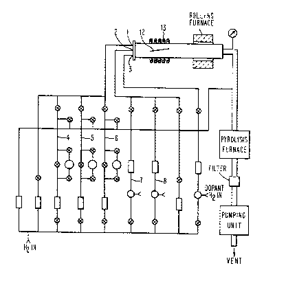
Brief Description of the Drawinqs
Figure 1 schematically illustrates a hot wall MOVPE
reactor and gas panel for use with the precursors of the
invention.
Figure 2 schematically illustrates a cold wall
MOVPE reactor and gas panel for use with the precursors of
the invention.
Detailed Description of the Invention
The present invention provides a method for
epitaxially growing III-V semiconductor compounds on a
semiconductor substrate by MOVPE in a hot wall reactor. The
invention utilizes precursors which possess both organic as
well as inorganic ligands on the metal bearing species. The
precursors are organometallic compounds of the form:
3o
2-y l+y
wherein
Y0988-017
~7~ 1313343
~l is a Group III metal atom,
R is alkyl or halo-substituted alkyl,
X is halogen, and
y is O or 1.
In accordance with the method of the invention, at
least one of the above organometallic compounds and at least
one compound of a Group V element are introduced into a hot
wall reactor of a MOVPE system under suitable temperature and
pressures to epitaxially deposit a III-V compound on a
semiconductor substrate. The Group III metal atom, M, may be
any of Al, Ga or In, and the Group V atom may be any of As, P
or Sb. For example, the alkyl or alkyl moiety contains 1-6
carbon atoms, preferably 1-3 carbon atoms, and especially
methyl and ethyl. Thus, the organic ligand may be any of
CH3, C2~5 or C3H5. The inorganic ligand, X, may be any of F,
Cl, I or Br. In addition, the organic ligand could have
halogen substituted for the H, for example, CF3 or C2C15.
The organic ligands fissure from the starting
precursor at low temperatures compared to that required for
epitaxial growth. The resulting species is of the form MX.
This species is stable at high temperatures and therefore, a
hot wall reactor system may be utilized in place of the
conventional cold wall reactor. The class of precursors of
the invention will not deposit the compound semiconductor
onto the reactor walls under a wide range of growth
conditions. The suppression of the growth on the reactor
interior walls further enables the use of a hot-wall reactor.
3o
In a hot wall reactor the use of RF induction or
radiant heating typically used in a cold wall reactor is
replaced by a furnace to maintain a temperature pre~erably in
the range of 200-800C. The hot wall system is a flow system
YO988-017
-8- 1~13343
in which source gases are introduced into the reaction
chamber and pumps are located on the reaction chamber to
maintain the operating pressure. The pressure is determined
by the amount and flow of the gas species in the chamber.
As shown in Figure 1, the Group III organometallic
halide vapors are supplied to the reactor from the gas panel
through entry port 1 and the group V source vapors are
supplied through entry port 2. The gas panel is the same as
is used in cold wall reactors and described in Kuech,
Material Science Reports V 2, 1987 page 6, incorporated
herein by reference. Depending upon the number of group III
elements in the semiconductor compound to be formed, the
corresponding group III organometallic compounds are supplied
to the reactor through entry port 1 via one of more of lines
4, 5 and 6. If only one group III element is in the
semiconductor compound then one line is used whereas if two
or three group III elements are in the semiconductor compound
then two or three lines, respectively, are used to supply the
different group III organometallic compounds. Similarly,
depending upon the number of Group V atoms in the
semiconductor compound to be formed, the corresponding group
V sources are supplied to the reactor through entry port 2
via lines 7 and 8. The reactor consists of a quartz tube 9
in a furnace 10. At higher pressures a throttled mechanical
pump is adequate whereas at lower pressures a turbo-molecular
pump is more suitable.
Volatizable elemental Group V species, Group V
hydrides or other Group V compounds are used as the source of
3 the Group V atom to form the III-V semiconductor compound. A
plurality of vapor flows are introduced into the reaction
Y0988-017
1313343
g
chamber including a Group III organometallic halide vapor
having a mole fraction in the range of .5 to 10 3and a Group
V source vapor having a mole fraction in the range of .5 to
10 3. The reaction chamber is heated and the Group III
organometallic halide vapor dissociates to form a metal
halide vapor which chemically reacts with the Group V
compound vapor to form the epitaxial layer. The thickness of
the epitaxial layers so produced depends upon the growth rate
and the time of deposition which are in turn generally
controlled by the temperature, reactor pressure and mole
fraction of the reactants.
- In accordance with another embodiment of the
invention, the hot-wall reactor is operated at very low
pressures, less than 10 torr, preferably in the range .001 to
torr. The low pressure conditions enhances the mass
transport of growth nutrients to the surface. Thus, the rate
limiting step to growth will be a temperature dependent
reaction. The low pressure also provides rapid transport of
the growth constituents to the growth surface. The
combination of low pressure and a hot wall system allows for
the high density stacking of the substrates into the hot wall
reactor and a highly uniform growth of the deposition over
the entire substrate surface. In the present invention,
batch processing of wafers can be achieved with excellent
uniformity of deposition, both on a wafer and from wafer to
wafer. For example, batch processing may be achieved in the
present system by vertical stacking of a large quantity of
wafers as shown at 11 in Figure 1. Such an arrangement
allows for a small interwafer spacing which may be as low as
3 1-10 millimeters. Thus, a high throughput of epitaxial
growth is obtained by use of the described class of
precursors in a hot wall reactor at very low pressures.
Y0988-017
--10--
131~343
Compound semiconductor structures may be grown
using the method of the invention in which there is a single
metal atom M and a single Group V element, such as GaAs, InP
and AlAs. Alloy compound semiconductors having multiple
Group III metal atoms may also be grown by introducing a
plurality of organometallic precursors into the system. For
example, the growth of compound semiconductors having two
Group III metal atoms, such as, AlxGal xAs where
O ~ x ~ 1, is accomplished through the introduction of both a
Ga and an Al bearing organometallic halide precursor such as
Diethyl Gallium Chloride and Dimethyl Aluminum Chloride. The
growth of AlGaP is similarly accomplished by substituting P
for As as the Group V atom. Furthermore, three Group III
organometallic halide precursors can be provided to form a
compound semiconductor having three Group III metal atoms,
such as, (AlxGal_x)yInl_yP where x is in the range O ~ x _1
and y is in the range of O ~ y ~ 1. Semiconductor compounds
containing two different Group III elements and two different
Group V elements are formed by providing two different Group
III organometallic compounds and two different group V
sources. A III-V compound of this form is InxGal xAsyPl y
where x is in the range O ~ x ~ 1 and y is in the range
O / y _ 1. Any Group III-V compound may be made by
introducing the appropriate precursors.
The process of the invention has further
application to the growth of heterojunctions through a change
in the composition of the gases inputted to the growth
reactor. The low pressure operation of the reactor allows
for the rapid exchange of gases in the reactor tube and hence
3 a sharp transition in the composition of the deposited films.
Through changing the flow of the Group III or Group V
YO988-017
--ll--
~3~3343
precursors into the reactor, changes on the cation or anion
sublattice are effected. Thus, heterojunctions of, for
example, AlGaAs/GaAs on a GaAs substrate may be formed
in-situ by first epitaxially grown GaAs in a first step and
then epitaxially growing AlGaAs in a second step by adding
the Al bearing precursor.
In-situ doping is possible by introducing dopant
source gases through entry port 3 at the time of introduction
of the Group III and Group V source gases, or during
interruptions in the epitaxial deposition. N and P type
doping is accomplished through the controlled introduction of
conventional gas compounds such as silane, disilane, dimethyl
zinc or other Group IIB, IV or VI compounds. The dopant
incorporation into the growing film is dependent on
temperature and pressure. The hot wall reactor operated at
very low pressures results in a highly uniform incorporation
of doped material.
In another aspect of the invention, the precursors
of the invention provide selective epitaxial growth of Group
III-V compounds on a masked substrate in an MOVPE system.
The class of precursors described herein containing a Group
III metal, an organic ligand and an inorganic ligand,
prevent any deposition on the mask. Complicated edge
morphologies are avoided and high quality Group III-V
material is left only in the unmasked areas. In accordance
with the method of the invention, a gaseous mixture including
at least one organometallic halide compound of a Group III
metal and at least one compound of a Group V element under
3 suitable conditions of temperature and pressure are
Y0988-017
-12- ~3~3343
introduced into a MOVPE reaction chamber having a masked
substrate to selectively deposit on the unmasked areas of the
substrate an epitaxial layer of a III-V compound
semiconductor.
The organic ligands fissur~ from the starting
precursors of the invention to provide a final reaction
product that is a metal mono-halgen, such as GaCl. Such
mono-halogen compounds have a strong metal-halogen bond that
allows for the decomposition of the compound to a stable
entity instead of free metal. The chemical entity does not
react on the masking mat~rial until very high super-
saturations are achieved. The nucleation of polycrystalline
material is strongly suppressed. Masking materials, such as
SiO~, SiNX, SiONX, A12O3 and AlN are used. In addition, the
halogen compounds, such as HCl, resulting as a growth
reaction by product in the growth environment, act to etch
and remove any small embryonic crystals from the mask surface
before a critical nuclei can be formed. These compounds
react to form mono-halogen precursors in the gas phase which
possess a high vapor pressure and do not adsorb strongly on
masking surfaces at typical MOVPE growth temperatures.
Selective epitaxy can be achieved in both a cold
wall system, as illustrated in Figure 2, and a hot wall
system as shown in Figure 1, under their respective operating
conditions. The cold wall system, similar to the hot wall
system, is a flow system in which the source gases are
introduced into the reactor chamber having pumps located on
the reaction chamber to maintain the operating pressure. The
3 pressure is determined by the amount and flow of the gas
species. For the cold wall reactor system, the temperature
is typically in the range of 500 to 800C and the pressure is
typically in the range of 1 to 760 torr.
YO988-017
-13- ~3~3343
In a cold wall system a plurality of vapor flows
is introduced into the reaction chamber including a Group III
organometallic halide vapor having a mole fraction in the
range of 10 3 to 10 4 and a Group V source vapor having a
mole fraction in the range of 5 to 1000 times greater than
the Group III organometallic halide vapor. The source of
heat in the cold wall system may be for example radiant
energy or rf induction to heat the susceptor to the growth
temperature. In Figure 2, heating is provided to vessel 12
by rf heating coil 13. The growth chemistry in the cold wall
system, as in the hot wall, is controlled by the temperature,
reactor pressure and mole fraction of reactants.
The use of at least one of the precursors of the
invention enables selective epitaxy without complicated edge
morphologies due to the diffusion of growth species from the
mask surface to the edge of the growing film. No deposition
is seen on the mask. Only high quality Group III-V compounds
are deposited in the unmasked areas.
The semiconductor materials that can be selectively
deposited include any combination of one or more Group III
elements of Al, Ga and In and one or more Group V elements of
As, P and Sb. Thus, any of the particular compounds
described earlier with respect to epitaxial growth on the hot
wall, low pressure system may be selectively deposited on a
masked substrate.
While the invention has been particularly shown and
described with respect to preferred embodiments thereof, it
3 will be understood by those skilled in the art that the
foregoing and other changes in form and detail may be made
Y0988-017
-14-
34~
therein ~ithout departing from the spirit and scope of the
invention which should be limited only by the scope of the
appended claims.
3o
Y0988-017