Note: Descriptions are shown in the official language in which they were submitted.
i~
YO987-099 DWC
~3~
TRANSPOS~BLE MEMORY ARCHITECTURE
DESCRIPTION
Technical Field
This invention describes a Transposable Memory
Architecture (TMA) for providing eaually fast
access to stored data in two or more dimensions.
This architecture is provided by orthogonal wiring
of access devices, word lines, and bit lines with
independent random accessing capability for data
in each direction. The TMA cell directly
implements the architecture using only two access
devices.
Background of the Invention
The use of matrix arrays of storage cells, along
~ 15 with the use of word lines for accessing a
; particular cell and bit lines for reading a
particular cell is well known in the art.
More specifically, U.S. Patent 4,287,575 to
Eardley et al. describes a storage cell
configuration in which each storage cell has
only two access devices, but the cells are
arranged in only a single dimension configuration.
U.S. Patent 4,447,891 to Kadota describes an array
of bit storage cells (memory cells) with two
complementary vertical word lines laddress lines3
and two complementary horizontal bit lines (data
YO987-099
~3~3l~
lines). The two complementary horizontal bit
lines (data lines) are connected through gate
elements to complementary input-output nodes,
while the gate elements are contro:Lled by the
vertical word lines (address lines). The word
lines being parallel and the bit l:ines being
parallel provides only single dimension accessing
of stored data.
i
U. S. Patent 3,693,169 to Kroy et al. describes a
three-dimensional storage system wherein all
storage positions are selectively accessible.
This system requires two conductors to open each
gate of the memory elements at the intersection of
these two conductors and still a thlrd conductor
for the transmission of an information signal.
.,
U. 5. Patent 4,494,231 to Slawy et al. describes a
memory module for a time division switching system
with parallel reading lines which are orthogonal
to parallel writing lines.
U. S. Patent 4,368,523 to Kawate also describes a
matrix of memory cells wherein the address buses
(word lines) are connected to the rows of the
memory cells in the matrix while the data buses
(bit lines) are connected to the columns of the
memory cells. The address buses run parallel to
each other in the horiæontal direction ~hile the
data buses run parallel to each other in the
vertical direction, thereby providing access to
data in only one dimension.
YO987-099
~3~3l,~l
A matrix memory module is also described in an
article entitled: A Rectangular Area Filing
Display System Architecture hy D. S. Whelan
appearing in Computer Graphics, Volume 16, No. 3;
pp. 356-362, July 1982. This article features
orthogonal addressing capability, but reads out in
only one direction in order to provide faster
rectangular area filling capability for display
systems. This module has two access devices in
series gated by row and column selects. This
module is read or written from a single pair of
bit lines only when both the row and column are
selected.
U. S. Patent 3,781,828 to Platt et al. features a
cell with two word lines, but both word lines must
be selected to read out data onto a single pair of
bit lines. The objective is to provide selection
capability to reduce the power dissipation in the
decoders and the array. Two word lines are
connected to the cell so as to incorporate an AND
function. A single pair of bit lines for reading
out in only one dimension is disclosed in this
application.
U. S. Patent 3,634,236 to Kolankowski et al.
features horizontal, vertical, and diagonal
accessing of a RAM array with vertical and
horizontal readout, but requires that both the
diagonal and either the horizontal or vertical
word line be selected for a readout of the data in
3Q any one cell. The above patent deals with data in
blocks, but does not provide readout from selected
YO987-099
~3~ 3~
blocks within a larger array~ Each cell in the
array has six access devicest three word lines,
and four bit lines. There is no description in
the above patent of transposable addressing
capability to a block of data within the RAM
array.
U. S. Patent 3,638,204 to Kolankowski et al.
features a cell with six access devices, four bit
lines, and three word lines for orthogonal
accessing and readout if and only if, two of the
three word lines are selec~ed.
U. S. Patent 3,490,007 to Igarashi features a cell
with four access devices, three word lines, one
pair of bit lines, and a sense line to provide the
lS well known associative memory function. The
normal one-dimensional-read and write path uses
one word line to gate two access devices onto the
dual rail bit lines in the ordinary manner. The
two extra devices, t~o word lines, and one sense
line are for checking a slice across the array
orthogonal to the bit lines for a valid compare to
some input bit external to the array.
Consequently, there are true and compliment word
lines for each cell gating two devices both onto a
single sense line. The read and write operatlon
described in this patent can only be done through
- a one-dimensional path with only sense capability
being provided through the orthogonal path.
U. S. Patent 4,541,075 to Dill et al. features a
second port to a standard DRAM array which can
YO987-099
~3 ~3~
asvnchronously read or write an entire row usinq a
row buffer register external to the array. Though
two output ports are provided, the data on the
second port is from the same dimens,ion as that on
the first port.
UG S ~ Patent 3,800,289 to satcher features multi-
dimensional access capability achieved with
address level manipulation. The memory array has
a single address selection input and a single
output path. This patent does not teach
orthogonal address capability implemented at the
cell/array level.
A]l of the art described above does not disclose a
memory system capable of providing single ended
reads with equally fast access to random data in
two or more dimensions.
Summarv of the Invention
It is therefore one of the objects of this
invention to provide for single-ended reading of a
bit storage cell or a group of bit storage cells
(data-unit~ in an array of such cells in either of
at least two dimensions.
It is also an object of this invention to provide
the above single-ended reading in multi dimensicns
using only one word line, one bit line and one
access device per bit per dimension.
YO987-099
~ 3 '~ 2 ~
It is a further object of this invention to
provide equally fast access to data-uni~s in more
than one dimension.
It i5 also a further object of this invention to
provide for transposition of data-units with only
a change in dimension address.
It is also a further ohject of this invention to
provide additional data path flexibility by
integrating multiple cell arrays in one TMA
device.
It is also a further object of this invention to
provide a method of writing a data-unit or a group
of data-units (data block) from only one data
direction with minimal cycle time penalty.
Accordingly, this invention provides a
transposable memory architecture device for a
memory access system. This device comprises a
matrix array of bit storage cells with n rows and
m columns. Dimension I word lines are also
provided for accessing the rows of the bit storage
cells in the array with each dimension I word line
being connected to a corresponding row of storage
cells. Dimension II word lines are used for
accessing the columns of the storage cells in the
array with each of the dimension II word lines
heing connected to a corresponding one of the
columns of storage cells in the array. The
dimension I word lines are orthogonal to the
dimension II word lines, and each storage cell in
the array is connected to a correspondina one of
YO987-099
..
~3~ 2~
the dimension I word lines and a corresponding one
of the dimension II word lines. In addition,
dimension II bit lines are used for detecting the
state of the bit storage cells in c:orresponding
rows of the matrix array. Each of the dimension
II bit lines is connected to the corresponding one
of the rows of the cells in the array. Dimension
I bit lines are also used for detecting the state
of cells in the corresponding columns of the
array. Each of the dimension I bit lines is
connected to corresponding one of the columns of
the array. The dimension I bit lines are
orthogonal to the dimension II bit lines, and each
bit storage cell ln the array is connected to a
corresponding one of the dimension II bit lines
and a corresponding one of the dimension I bit
lines. The state of a selected one of the storage
cells can be detected from either of two
orthogonal directions by accessing the selected
cell with either one of the dimension I word lines
connected to the cell or with one of the dimension
- II word lines ccnnected to the cell, and by
detecting the state of the selected cell by
reading the voltage on either the dimension II bit
line connected to the seLected cell or the
dimension I bit line connected,to the cell. It is
particularly important to note that each cell in
the array is connected to onl~ a single dimension
I word line, a single dimension II word line, a
single dimension I bit line and a single dimension
II bit line. Multiple bit-lines may be selected
in either or both dimensions to provide a
YO987-099
~ 3 ~ ,C~, ~
data-unit from multiple cells along one word line
in either or both data directions.
kloreover, this invention provides a multiple
transposable memory architecture cevice for
reading data stored in the device by accessing the
data in mutually orthogonal directions where more
than one data-unit may be read from the device at
the same time and where more than one data~unit
may be written in the device at the same time.
This device comprises a matrix of Tk'~ cell arrays
naving N rows and M columns of such T~IA cell
arrays. Each i-th array in turn, has a ni x mi
array o bit storage cells. Each TMA cell array
has an associated dimension I word line decoder,
dimenslon II word line decoder, dimension II bit
line decoder and dimension I bit line decoderO
Each i-th dimension I word line decoder is
connected to ni dimension I word lines. Each
dimension I word line is used to access the
corresponding row of bit storage cells in a
corresponding one of the TMA cell arrays. Each
i-th dlmension II word line decoder is connected
to mi dimension II word lines, and each of the
dimension II word lines are used to access a
corresponding column of the bit storage cell~ in a
corresponding one of the Tk~ cell arrays. Each
i-th dimension I (dimension II) word line decoder
is used to access cells on that row by placin~ a
high or low voltage on selected ones of ni
dimension I (mi dimension II) word lines. Each
i-th dimension II bit line decoder is connected to
ni dimension II bit lines, and each dimension II
YO987-099
~3~3~
bit line is used to detect or establish the state
of a first bit storage cell in a corresponding row
of cells in a corresponding one of the TMA cell
arrays~ This first cell can be a cell which has
been accessed by a dimension II word line
corresponding to the column in which the first
cell is located~ Each i-th dimension I bit line
decoder is connected to mi dimension I bit lines,
and each of the dimension I bit lines is used to
detect or establish the state of a second blt
storage cell in a corresponding column in a
corresponding one of the T~lA cell arrays. This
second cell can be a cell which has been accessed
by a dimension I word line corresponding to the
row in which the second cell i5 located. Each
i-th dimension I (dimension II) bit line decoder
is also used to select a subset in a set of mi
dimension I ~ni dimension II) bit lines.
; Brief Description of the Drawings
FIG. 1 is a schematic illustration of the
transposable memory architecture device or TMA
cell array of this invention.
, ' ,
FIG. 2 is a schematic illustration of a bit
storage cell (or TMA cell) used in this invention.
FIG. 3 is a schematic of a multiple transposable
memory access device.
.
YO9~7-099
~3~ 2~
FIG. 4 is an array of data bits showing data units
extending in the horizontal and vertical data
directions (also known as dimension I or dimension
II data direction).
FIG. 5 is a block diaqram illustration of the
transposable memory architecture device includina
the decoders and lnput and output circuitry. This
device is a matrix of T~ cell arrays havins two
rows and two columns or four quadrants.
FIG. 6 is a timing diagram which illustrates a
method of writing in a TMA cell array.
Description of the Prererred m o iment
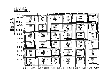
Shown in FIG. 1 is a matri~ array of bit storage
cells with the array having n rows and m columns.
In this figure n = m = Ç, but any suitable inte~er
may be used, and n need not equal m. Each bit
storage cell 20 is connected to a pair of word
lines and a pair of bit lines. Each pair of word
lines consists of a dimension I word line (WLI)
and a dimension II word llne (WLII) with the
dimension I word line being orthogonal 'o the
dimension II word line. Each bit storage cell qQ
is also connected to a pair of bit lines. Each
pair of bit lines consists of a dimension II bit
line (BLII) and a dimension I bit line (3LI) with
the dimension I word line bein~ orthcaonal to the
dimension II word line. Each dimension I worc
line is connected to a corresponding row of bit
storage cells in the array. Each dimensicn I word
~0987-099
~ 3 'L ~
line is used Lor accessing the corresponding ro~
of bit storage cells in the array. Similarly,
each dimension I word line is connected to a
corresponding column of bit storage cells in the
arrav, and is used to access that corresponding
column of bit storage cells in the array. The bit
lines, on the other hand, are used to detec' the
state of corresponding bit storage cells in the
array. A bit line (dimension I or II) is also
used to write in the state o~ cell which has been
accessed by a corresponding word line (dirnension I
or II). As with the dimer.sion I word lines, each
dimension II bit line is connected to a
corresponding one of the rows of bit storage cells
in the array. Also, each dimension I bit llne is
connected to a corresponding one of the columns or
bit storage cells in the arra~. Also shown in
FIG. 1 are six dimension I word lines WLI-l
through llLI-6 extending in the horizontal or
dimension I data direction. Additionally shown in
FIG. 1 are six dimension II word lines ~LII-l
through WLII-6 extending in the vertical or
dimension II data direction. Also shown in FIG. 1
is the dimension I data direction which is the
horizontal direction and the dimension II data
direction which is the vertical direction. The
corresponding bit lines for each dimension can
also be seen in FIG. l; BLI-l through BLI-6 extend
in the vertical direction ana BLII-l through
BLII-6 extend in the horizontal direction.
Shown in FIG. 2 is the bit storage cell (20) used
in the preferred embodiment of this invention.
YO987-099
The bit storage celi ~also known as a TMA cell)
has a CMOS latch (25) with devices T1~ T2, T3 and
T4. The storage cell also has two NMOS access
devices TAl and TA2. However, the access devices
could also be PMOS devices, while the latch could
also be a PMOS latch or an NMOS latch with either
dynamic storage or resistive loads. Also shcwn in
FIG. 2 are dimension I and dimension II t.~ord
lines, connected to access devices ~A1 and TA2
respectively. More specifically, as an example,
dimenslon I word line WLI-l and dimension II word
line WLII-3 are shown. Also shown are the
dimensi.on I and II bit lines connected to TAl ~nd
TA2 respectively~ Again as an e~ample, dimension
I bit line BLI-1 and dlmension II bit line Bl,II-3
are shown. The word and bit lines specifically
mentioned above correspond to the bit stora~e cell
in the first row and .hird column of the matrix
array of bit storage cells shown in FIG. 1.
For the purposes of reading and writlng, the terms
(word line) and (bit line) are used in the
conventional sense. 17hen the word line ls
selected, the state of the cell is read out cr.to
the bit line, or the state o f the bit line is
written into the cell. For exa~ple, when t~e
dimension I word line is selected, the state of
node 1 may modulate the voltage level o~ the
dimension I bit line. The dimension II word l ne
of the same cell, or another cell, may be
simultaneously selected in order to allow the
state of node 2 to modulate the voltage ievel o f
the dimension II bit 'ine. To write any one cell,
`1098,-099
3 ~
however, both word lines and both bit lines need
to be driven either simultaneouslv or
sequentially. The single ended procedure for
reading and the dual ended procedure for writing
the bit storage cell will be described below.
As in a conventional RAM, the state of several
cells (a data-unit) associated with the same word
line may be read simultaneously by selecting
several bit lines. In most applications, the
higher bandwidth provided by a multi-bit data-unit
is the pre erred embodiment. With a TMA device a
data-unit from either or both dimensions may be
accessed in one cycle. With the TMA cell the
cycle time to read a data~unit is nearly
equivalent to that for a conventional ~AM.
Additionally, the TMA cell array provides dual
dimensional access capability with very little, if
any, increase in area relative to a conventional
cell.
20 A preferred embodiment of a Transposable Memory
Architecture (TMA) or a Multiple Transposable
Memory Architecture (MTMA~ device is shown in FIG.
3 with the input and output ports indicated. The
data-unit which is read is output throuah port 38;
25 the data-unlt to be written is input through port
37. A data-unit is selected from the TMA array by
word and bit addressing throu~h ports 31 and 33
unaer control of the chip-select 39 and
write-enable 34 inputs in the conventional manner~
YO~87-099 ~
.
~ 3 ~
14
In contrast to the conventional memory
architecture, an additional address - the
"dimension address" - (received through input port
35) defines the dimension from which the data-unit
is to be selected or, possibly, to which it is to
be written. FIG. 4 illustratas the transposition
of the data-unit that r~sults from switching ~he
dimension bit while keeping the ~ord and bit
addreeses fixed. Suppose, for e~ample, a
particular address plus a "1" dimension bit state
results in the third data-unit (42) of dlmension I
being read, which is in the third row of the FIG.
4 data block. Then, switchin~ the dimension bit
to the "0" state wikhout changing the word or bit
address r~sults in the third data-unit ~44) of
dimension I~ being read, which is the third column
of the FIG. 4 data block. Accomplishing the same
transposition in the case of 3 conventional memory
architecture, would require many cycles of the TMA
device; typically, the number of cycles required
would be equal to the width of the data-unit (8 n
FIG. 4).
A more detailed block diagram of a multip'e T~A
device is shown in FIG. 5. A basic single-arra~
TMA device 30A(delinea~ed by dashed box) consists
of an array of TMA cells (FIGS. 1 & 2), a word and
bit decoder for each dimension (52, 54, 56, 58),
input circuits 51, 53 and 55 for the address ports
31, 33 and 35 and input circuits 59 for
chip-selec~ port 39, and data inpu~ circuits 57I
for ports 34 and 37 and output circuits 570 for
driving outpu~ port~ 38. Again referring to FIGS.
~;~
`~C9~7-099
~3ll~
3 and 5 input circuits 51, 53, 55, 57I, and 59
detect the state of associated input ports and
drive buses to distribute signals within the MTMA
device as indicated in FIG. 5. More specifically,
input circuit 51 cletects the state of the address
bits to input port 31 and drives the address
inputs tc corresponding word line decoders 52 and
53. Also, input circuit 53 detects the state of
the bit addresses at input port 33 and drives the
address inputs to dimension I bit line deccders 58
and dimension II bit line decoders 56. Input
circuit 55 detects and amplifies the state of the
dimension bit at the input port 35 and the output
of circuit 55 enables corresponding dimension I or
lS ~imension TI deco~ers. Data output circuits 570
ampli~y the state of data transmitted to its
inputs from corresponding bit line decoders and
drive a corresponding data output port 38. Also
shown in FIGS. 3 and 5 is chip-select input port
39, Input circuit 59 detects the state of port 39
and provides drive for the cl~ck signal which
results in all the peripheral circuitry going from
a standby or precharge state to an active state,
and therefore, in data being read or written.
FIGS. 3 and 5 also show write-enable input port 34
which is used to control the data-in circuitry so
that the data-in state is force~ into selected
cells through the bit lines in the case cf a
write, or so that the state of the cell can be
detected through the ~it lines in the case of a
read. Standard RAM peripheraI circuits and logic
can be used for the above described ~unctions;
YO987-~9~ i
q~ ~ ,p
~ 3~3~
l6
they therefore will not he shown in further
detail.
In FIG. 5 the lines interconnectinq the address
input circuits, decoders, and array indicate that
the same word and bit addresses are used for each
dimension. The dimensional bit is used to
selectively enable the dimension that will h~
sensed, amplified, ar.d bussed through the bit
decoders and output circuitry to the device
outputs, or that will be written under control of
the data-input circuitry (includes write-enable
inputs). The dimension address input need oniy
select which bit-decoder dimension output Ls
connected to the data-output circuitry. This
selection can happen late in the critical path
and~ therefore, have minimal impact on read access
time. However, a power and di/dt ~rate of
change of current) savings could result rro~ also
selectively enablin~ the word decoders and the
s~nse circuits in the bit decoders~ In this
latter case, the bit-~ecoder outputs may be simply
dot-ORed.
A mùlti-array version 30 of the TMA device,
referred to as a multiple trans~o~able memor~
device (MTMA), is also shown in FIG. 5.
multi-array design is preferred for speed and for
data-path versatility. If, however, power ~nd
area are more important, a sir.~le-array trersion
may be preferred. For the multi array case,
peripheral circuit area could be minimized bv
sharing some of the decoders and inpu~ circuitry
J~ ,~Ji'~
~'0987-099 ~
~3~3'~
across adjacent array boundaries, as shown in FIC.
5. The matrix of TMA cell arrays (shown in FIG.
5) has two (N) rows and two (M~ columns. Each
i-th cell array in turn has an arra~ of bit
storage cells with ni rows and mi columns. For
the case shown in FIG. 5, i would be an integer 1
~ i s MxN where i designates a speci.ic array. ni
and mi designate the number of rows and columns,
respectively, in the i-th array. Each TM~ cell
array 50 has an associated pair of word line
decoders, a dimension I word line decoder 52 and a
dimension II word line decoder 54. The i-th
dimension I or II word line decoder is associated
with the i-th cell array with the dimension I word
lS line decoder connected to ni dimension I word
lines and with the dimension II word line decoder
connected to mi word lines. ~ach i-th dimension I
word line decoder selects a dimension I word line
from ~he set or ni dimension I word lines and
places a high or low voltage on that selected
dimension I word line. This selected dimension I
word line then accesses a corresponding row of bit
storage cells in the i-th TMA cell array. In a
similar manner, each i-th dimension II word line
decoder selects one of a set mi dimension II word
lïnes and places a high or low voltage on that
selected dimenEion II word line which in turn is
used to access a corresponding column of bit
storage cells in the i-th TMA cell arra~-. Each
TMA cell array 50 also has a pair or bi~ line
decoders, a dimension II bit line decoder 56 and a
dimension I bit line decoder 58. The i-th
dimension I or dimension II bit line decoder is
'~
YO987-099;~ '~
~ 3 ~ 3 ~ L
18
associated with the i-th c~ll array with the
dimension I bit line decoder connected to mi blt
lines and witll the dimension II bit line decoder
connected to ni bit lines. Each i~th dimension I
bit line decoder is used to select one of the m.
dimension I bit lines, and the selected dimension
I bit line is used to detect or establish the
state o~ storage cells in a correspcnding column
of cells in the i-th TMA cell arrayO Similarly,
each i-th dimension II bit line decoder selects
one of the ni dimension II bit lines, and this
selected line is used to detect or estab]..~sh the
state of bit storage cells in a ccrresponding row
of cells in the i-th TMA cell arrav. Tn th~
above, the actual cell or ~roup of cells
(data-unit) whose state is detected or established
depends upon which cells in the respectlve row or
coltlmn has been accessed by a correspondin~
dimension I or II word line. Detecting the state
of a cell corresponds to read~ng the cell, while
establishing the state of a cell corresponds to
writing a bit in the cell.
Evident from FIG. 5 is the orthogonal placement o.
the dimension I word and bit decoders 52 ar.d ;8
~elative to the dimension II word and bit decoders
54 and 56~ It is understood, however, that there
are other embodiments which may be better suited
to other applicatior.s. The bloc~ dia~rams o
FIGS. 3 and 5 sho~7 the preferred embodime~t ~ith
data~in port(s) 37 and data-out port(s) 38. Other
embodiments could have separate data-out and/or
data-in ports for each dimension, since it is
~,~
~0987 099 .~
~3~3~;2~
1~
possible to simultaneously read or wrl~e th~ a.ray
frcm both dimensions. Other ~AM options known in
'he art, such as variations in the control inputs,
could be applied in the design of a T~-1~ device fcr
a particular application.
An alternate embodiment of the ~lTMA device could
use the multiple arravs to provide rapid accessing
of data in more than two~dimensions. Dedicated
data-in buses along with dedicated decoders to
each array could provide a shifting of data
written-into one array relative to the same data
written into another array. If n arrays are thus
used, then a read access through the TMA arrays
could provide any one or all of 2r. data-units from
2n dimensions simultaneously.
Read Operation
Due to the independent selection, cell access, and
sensing means provided for each dimen~ion, any one
data-unit can be read in one dimension while any
one data-unit is being read in the other. A cell
is said to be accessed when either one of the
access devices TAl or TA2 is turned on. For a
read to either dimension, a single-ended read
proceduxe is used, as follows:
5 1. In standby, all word lines are low ard all bit
lines are high ("high" may be ~ub~tantially
below VDD, depending on the details of the
application~.
~0987 ~ ~J ;~
~ 3 ~
2. Prior to ~ read~access, a drive means to the
bit lines are switched so as to have a much
higher impedance than can be provided ~J the
cell zero-state. For example, either the bit
line drive is turned-off and the large Li'
line capacitance is left floating, or a small
load device is turned-on to ~imit the bit line
swing in case a zero-state is read.
3~ The word line which was selected by a word
line decoder dimension I or II r~eans extern~l
to the array is drivell to a high voltaae,
thercby turnlng-on the associated acce~s
devices. That is, a high voltaqe is placed o
the word line Gèlected b~ the ~ord line
lS decoder.
4. The bit line is either unchanged lone-state~
or it is discharged towards ground
(~ero-state), depending on the state of the
storage latch. Whether the bit lir.e state is
to be interpreted as a one-state or zero-state
depends on the dimension being read. ~.s an
example for dimension I:
a. ~ one-state corresponds to the atch
device Tl being off and the
bit line voltage being unchanged.
b. A ~ero-state corresponds to the la~ch
device Tl being on and the bit
line voltage being pulled-low.
. 1
YO987-099 ~; !~
~L3~3~ ~
P~elative to the dimension I e~ample Lor
dimensions II:
a. A one-state corresponds to the latch
device T2 being on and the
bit line voltage being pulled~low.
b. A zero-state corresponds to the latch
device T2 being off and the bit
line voltage being unchanged.
5. The bit line decoders (dimension I or II) have
a bit line sensing and decode means which
amplify a selected bit line state ~or a group
of bit line states) by comparison to a
reference voltage and gates the approprlate
bit-states to the data-out pins. The cecoders
also serve to select ~hich bit lines are to be
read as described above.
The reference voltage can be derived in many ways,
the simplest being a threshold drop below the bit
line high voltage. The detailed design of the
re~erence voltage generator and sense amp is too
dependent on the details of any one application to
~e worthwhile describing here. Standard MOS SRAM
and DRAM circuit techniques can readily be used
(as is also the case with the other array
selection and sensing means). However, the
reference voltage design is not as critical as it
is in the DRAM ca~e, since the TMA cell provides a
continuous read out current instead of the small
.
,
'fO9~/-099 ~' ,~ -
J~1
bit line voltage charge provided bv the ~R~r~
charge transfer read-out.
Write Oper~tion
In any static RAM cell, switching the state cf the
latched st.orage means requires pulling-down the
high storage node. The latch can no' be switched
by pulling-up the low node through the access
device (TAl or T~.2 in FIG. 1) since it must be
designed to have a smaller current ~arrvinq
capabil.ity than the latch device (Tl or T2) ln
order to give a stable read. Consequentl~, i.n
the TMA cell, hoth word lines to any one ceil need
to be selected in order -to order to insure ~ ~,rite
of that cell, although both word lines co llCt have
lS to be selected simultaneously. Also, as ~r. a
conventional static RAM, a stable write requires
that the access device (TAl or TA2) size be
designed to have a lower on-resistar.ce than ~he
load device (T3 or T4), 90 that the intcrnal cell
node (node 1 or 2~ can be forced low.
To write one TMA cell is straight_orward an~.
consistent with previouslv described methods:
word lines for bpth dimellsions are brouqht hic,h
while the bit line for each dimension is ~leld at
either a high or a low voltage, depending on '~.e
state to be written. To prevent distur~ance of
cells which are not supposed to be writter., cnly
one cell at a time can be written simultar.eously
from both dimensions. Consequently, tc write a
data-unit largPr than one bit by con~entional
;
Yog~7-O99'~
1313~ L
methods, multiple cycles are required. For
e~ample, writiny an 8-bit wide data~unit requires
- one cycle of the word line for the dimension in
the data direction being written, but 8 c~cles for
the 8 word lines in the other dimension. If
data-in ports are available for each dimension,
the same ~ cycles can be used to write an 8 by 8
bit data block (which is the same number of cycles
required to write that data block in a
conventional one-dimension RAM). However, if data
is supplied for only one dimension, as is the case
for ~he preferrecl embodiment, FIG. 3, latches
exterral to the array and extra c~cles are needed
to store the data ~or the other dimension. In
this case, the number of cycles needed to wlite an
n x n data block i9 2n-1, or 15 in our 8 X 8 bit
data block example.
However, using a new write method, for the
preferred embodiment, a data-unit can be written
in one cycle, or x data-units in x cycles,
regardless of the number of bits corstituting a
data-unit. Thus, this made allows write-time for
the preferred embodiment of the T~A device tc be
about the same as for a conventional RA~l. The key
Ceatures of the preferred embodiment are a sin~le
data-input port (in other words, data for one
dimension only) and a CMOS TMA cell ~or any other
version of the cell with a strong enough pull-up
device to ~eet the cycle time requiremer.ts).
Briefly, the proc~dure is to preset the
data-unit(s) to be written by discharging all
internal nodes on the side accessed l~y the
~0~87-~99
24
dimension for which data-in is no~ supplied. ~hen
each data-unit in the block which was preset can
be written according to the state of the data-ln,
wlth one c~cle for each data unit.
For a more particular example, referring to
Figures 1 and 6, suppose the data-unit is t~o bits
(2-bits i~ used for description con~renier.ce Gnlt~;
2 much larger data-unit may be preferred fcr
actual applications~. Also suppose for this
write, the word, bit, and dimension addresses
select WLI-l and BLI-1. In other words, the first
two cells in the first row of FIG. 1 are to be
written through the di~ension I data direction.
~150 suppose that the write-enable input cont-ol
hits indi.ca~ that two sequential words will be
written. To preset the array at the beginniny of
the cycle, WLII-l and WLII- are simultaneously
pulsed while BLII-l and BLII-2 are both held low.
This s~ts all four cells in the selected data
block to have high voltages on the side to be
accessed in the dimension I data direction (node
1). (During the preset operation, unselected bit
lines are all held high, preventing disturbances
of other cells on the sclected word lines~. Then,
~ILI-l can be pulsed high while ~LI-l is ileld hi~h
or low, depending on whether the data-in is 1 or
0. In the second cycle WLI-2 is pulsed while
BLI-2 is held high or low, dependina on l;nether
the data in i5 1 or 0. Note that writ~n~ 'he
second dat~-unit does not require another preset,
assuming a write-enable control or a hardwired
specification is available to define the cepth or
,~'
!.'
YC987-0~9
~ 3 ~
the data-block, which would be the preferred
embodlment. The above described pulse sequence is
shown by the waveforms of FIG. 6.
he preset time may ex~end the write cycle time
S for at least the first data-unit written in a
data-block~ However, the preset can be overlapped
with the time required to sense the data-in state
and to drive the data-in busses for the
data-direction being written. It can also overlap
the time needed to pre-charge the bit lines in the
data-direction being written. The word line pulse
for the pre-set can overlap the word line pulse
for the write, as long as the non-overlap time Eor
both word lines is long enough so that an .internal
cell node can have charged high enough to hold the
written cell state. This is the case shown in
FIG. 6.
The CMOS version of the TMA cell is the preferred
embodiment ror all the same reasons that it is
becoming the preferred type in the general SRAM
market. This new mode of writing 'he CMOS TMA
cell greatly enhances the advantage offered by TMA
for write-intensive applications. Thus, the TMA
de~ice supplies dimensional tra~lsposition of data
with very little, if any, penalty in read or write
speed relative to a standard one-dimensional RAM.
:
`