Note: Descriptions are shown in the official language in which they were submitted.
~ 313~22
Specification
Title of the Invention
Cache Memory Control System
Background of the In en_ion
The present invention relates to a cache memory
control system.
Cache memories are small-capacity, high-speed
buffer memories arranged between processors and main
memories and are very popular in medium and high speed
computer systems for effectively shortening main memory
access time under the control of processors.
The principle of cache memories is described in
detail in Computing Survey, Vol. 14, No. 3, PP. 473 - 530,
1982 and is based on an empirical rule wherein "locality"
is present in main memory,access, i.e., referencing of a
main memory address space by a program.
The above reference describes "locality means
that the loci of reference of the program in the near
feature are likely to be near the current loci of
reference." By utilizing this property of locality, the
co~tents of successive memory locations (to be referred to
as a block) having a predetermined size and including a
word currently accessed from the CPV to the main memory are
fetched from the main memory to the cache memory. Only
high-speed cache memory access is then required, and
low-speed main memory access need not be performed.
-- 1 --
~3~3~
Conventional cache memories have the following
disadvantages.
Each entry of the cache memory consists of data,
an address tag representing a data location in the main
S memory or a real address, and a valid bit representing
validity of the data. Since the cache memory comprises a
random access memory (RAM), valid bits of all entries must
- be cleared when the cache memory system is powered or the
virtual address space is changed. A conventional cache
memory system includes a controiler which controls the
clearing of the valid bits in accordance with a power-on
signal or an instruction from the processor and
acknowledges the end of clearing to the processor. The
processor starts using the cache memory in response to a
clear end acknowledgement signal from the controller In
this valid bit clear control system, the end of the
clearing must be detected by the processor and the
processor determines whether the cache memory can be
accessed, thus undesirably increasing the overhead of the
processor.
The conventional cache memory has another
disadvantage as follows.
Whenever a main memory in a conventional computer
system is accessed, an error check must be performed in
units of data. During data transfer from the main memory
to the cache memory, the error check in units of data is
applied. T~e data to be transferred include data which is
-" ~ 3 ~ 3 ~ 2 ~
7118~-83D
not employed by the processor. Therefore, the above data check
indicates that unnecessary error check is performed.
_ummary of the In~ention
It is an object of the present invention to provide
a cache memory control system for decreasing the overhead during
the operation of a cache memory under the control of a processor
when a memory is powered or a virtual address space is changed.
It is another object of the present invention to
provide a cache memory control system for preven~ing a processor
from performing unnecessary error checking during data transfer
from a main memory to a cache memory.
A cache memory control system according to an aspect
of the present invention comprises a small-capacity cache memory
arranged between a processor and a main memory to effectively
shorten access time; means for detecting error information
representing an error occurring during transfer of a block from
said main memory to said cache memory; means for outputting a
timing signal representing a transfer timing of processor access
data accessed by said~processor, the processor access data being
included in blocks transferred from said main memory to said cache
memory; and error information retaining means for retaining the
error information when the error information detected by said
detecting means is discriminated by the timing signal such that the
error information is associated with the processor access data,
and for sensing a discrimination result to said processor.
- 3 -
~31~2~
71180-83D
Brief Description of the Drawings
Figure 1 is a b~ock diagram of a cache memory
control system according to an embodiment of the present inven-
tion;
Figures 2(A) to 2(F) are timing charts showing
waveforms of signals in the main parts in the circuit shown
in Figure l;
Figure 3 is a block diagram of a cache memory control
system according to another embodiment o~ the present invention;
and
-- 4 --
~3~3'~
Figs. 4(A) to 4(J) are timing charts showing
waveforms of signals in the main parts in the circuit shown
in Fig. 1.
Detailed Description of the Preferred Embod_ments
Preferred embodiments of the present invention
- will be described in detail with reference to the
accompanying drawings.
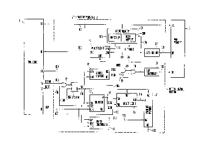
Fig. 1 shows a cache memory control system
according to an embodiment of the present invention.
Referring to Fig. 1, a cache memory unit 2
including a cache memory 20 is connected between a
processor 1 and a main memory 3. The cache memory 20
includes a directory 20A and a data memory 20B and is
connected to an address bus 101 for connecting a terminal
lA of the processor 1 to a terminal 3A of the main memory
3. An output of the cache memory 20 is connected to a
terminal 23A of a multiplexer 23 through a line 119.
A data bus 121 of the main memory 3 is connected
to the input terminal of the cache memory 20 and an input
terminal 23B of the multiplexer 23 through a latch circuit
22. The multiplexer 23 selects the signal input to the
input terminal 23A or 23B in response to a control signal
input to a control terminal 23C. The selected signal is
output from an output terminal 23D to a data bus 102 of the
processor 1.
An output terminal lC for a signal representing
access status of the processor 1 is connected to an input
.. ..
~3~3~
terminal 15A of an access changer 15 through a line 103.
The access changer 15 activates the output signal from a
terminal 15C or 15D in response to a control signal
supplied to a control terminal 15B. The output terminal
15C of the access changer 15 is connected-to one input
terminal of an AND gate 18, and the output terminal 15D is
connected to one input terminai of an OR gate 19. The
other input terminal of the AND gate 18 receives a signal
MISS representing that data requested by the processor 1 is
not stored in the cache memory 20~ An output from the AND
gate 18 is input to the other input terminal of the OR gate
19. An output from the OR gate 19 is input to the control
terminal 23C of the multiplexer 23 through a line 118 and a
bus controller 21. The bus controller 21 is connected to a
control terminal 3C of the main memory 3 through a line
122.
: Reference numeral 11 denotes a valid bit memory
for storing valid bits; 12, a counter for counting
addresses for data to be cleared in the valid bit memory
11; 13, a write controller for controlling write access of
the valid bit memory 11; and 14, a register for maintaining
a p~edetermined state during clearing. Although the.valid
bit memory 11 is part of the directory 20A in the cache
memory 20, the memory 11 is separately shown for the
illustrative convenience.
The address bus lQl of the processor 1 which
outputs an address signal for the valid bit memory 11 is
- 6 -
. ; . . : .
13~3~
connected to one input terminal 16A of the multiplexer 16
through a line 104. The other input terminal 16B, a
control terminal 16C, and an output terminal 16D of the
multiplexer 16 are respectively connected to an output
terminal A of the counter 12 through a line 111, an output
terminal Q of the register 14 through a line 110, and an
input terminal A of the valid bit memory ll through a line
114. The multiplexer 16 selects the signal input to the
input terminal 16A or 16B in response to a control signal
S14 supplied to the control terminal 16C. The selected
signal is output from the output terminal 16D. The control
signal S14 output from the register 14 through the line 110
is also supplied to enable terminals EN of the counter 12
and the write controller 13 and to a control terminal WD of
the valid bit memory ll.
A clear command signal CLEAR output from an
output terminal lE of the processor 1 and representing
clearing of the valid bit memory 11 is input to one input
terminal of an OR gate 17. A reset signal RESET output
from an output terminal lF of the processor 1 is input to
the other input terminal of the OR gate 17 and to a reset
terminal RST of the counter 12. The output terminal of the
OR gate 17 is connected to a set terminal S of the register
14. A reset terminal R of the register 14 is connected to
a terminal END of the counter 12 through a line 112. The
terminal END outputs a signal S12B representing the end of
counting of the counter 12.
-- 7 --
, :., ~. . ';'' ': , ;; , ,
" ~3~ ~2~
An output terminal lG for a clock signal CLK of
the processor 1 is connected to clock terminals CLK of the
counter 12 and the write controller 13 through a line 107.
An output signal Sl3 from the write controller 13
is supplied to a write terminal WR of the valid bit memory
11. A read terminal RD of the valid bit memory 11 is
connected to a HI~/MISS signal generator ~not shown) in the
cache memory 2Q through the line 122.
The operation of the circuit shown in Fig. l will
be described with reference to Figs. 2(A) to 2(F)
representing waveforms of signals in main parts in the
circuit.
When the clear command CLEAR or the reset signal
RESET is not output fxom the processor l, the register 14
is maintained in the reset state, and its Q output signal
S14 is set at high level ("H"). In this case, the cache
access mode is set. In this mode, the write controller 13
is kept disabled. An address signal for the valid bit
memory 11 is supplied from the terminal lA of the processor
1 through the multiplexer 16. At the same time, the access
changer 15 sets an output signal S15A at "~" level.
However, if the signal MISS is not output, an output signal
from the AND gate 18 is kept at low level ("L").
Therefore, an output from the OR gate 19 is kept at "L"
level. The multiplexer 23 selects the output from the
cache memory 20, and the selected signal is output onto the
data bus 102 of the processor l. During this operation,
13~3~
the bus controller 21 inhibits access of the main memory 3O
When the signal MISS is generated in the cache access mode,
an output from the AND gate 18 and hence an output from the
OR gate 19 are sequentially set at "H" level. The
multiplexer 23 selects an input at its input terminal 23B.
At the same time, the bus controller 21 starts access of
the main memory 3. The data from the main memory 3 is
supplied onto a line 120 from the latch circuit 2~ to
update the contents of the cache memory 20.
When a signal ~IT is delivered from the cache
memory 20, the multiplexer 23 selects data output from the
cache memory 20 through the line 119, and the selected data
is output onto the processor data bus 102.
; The cache bypass mode as the characteristic
feature of the present invention will be described below.
When the register 14 is set in response to the
reset signal RESET or the clear command CL~AR from the
processor 1, its Q output, i.e., a signal S14 which
represents the clear period enables the counter 12 and the
write controller 13. The respective operations of the
counter 12 and the write controller 13 are started. An
out~ut S12A from the counter 12 is supplied as an address
signal to the valid bit memory 11 through the multiplexer
16. A memory location addressed by the signal S12A is
cleared by a signal S13 from the wri~e controller 13.
Valid bit clearing is completed, the counter 12 outputs the
clear end signal S12B. The register 14 is xeset in
, ~,3~3l,~C~
response to the clear end signal S12~, and therefore the
counter 12 and the write controller 13 are disabled.
When the output signal S14 from the register 14
is sek active, the output terminal 15D of the access
changer 15 is set active ("H"~. An output from the OR gate
19 is set at "H" level, and the multiplexer 23 selects an
input signal at its input terminal 23B. At the same time,
the bus controller 21 outputs a control signal to the main
memory 3, thereby starting access of the main memory 3.
The data read out from the main memory 3 is
latched by the latch circuit 22 and is output onto the
processor data bus 102 through a line 117 and the
multiplexer 23.
As described above, according to this embodiment,
during clearing of the valid bit memory 11, the mode of
access of the cache memory 20 by the processor is
automatically changed to the bypass mode at the cache
memory unit 2 side or to the cache access mode at the end
of clearing of the valid bit memory 11. Therefore, the
processor 1 can access the cache memory 11 without
detecting the end of clearing of the valid bits.
Fig. 3 is a block diagram of a cache memory
control system according to another embodiment of the
present invention. Referring to Fig. 3, reference numeral
25 40 denotes a processor; 50, a cache memory; and 70, a main
memory. The cache memory 50 includes a directory 51 and a
data memory 52.
- 10 -
`` ~31~3~2~
An address bus 201 of the processor 40 is
connected to the input terminal of a:n address register 53.
The output terminal of the address rlegister 53 is connected
to the cache memory 50 and an I/O buffer 54 for
time-divisionally controlling the inputs to or outputs from
the main memory 70. The I/O buffer 54 is connected to the
main memory 70 through a bidirectional bus 203 and
time-divisionally gates the address signal supplied to the
main memory 70 and data output from the main ~emory 70.
A data output from the I/O buffer 54 is input to
and held by an input register 55. The input register 55
outputs the data to the cache memory 50 and a bypass
register 56 in response to a control clock signal c input
through a line 207. The bypass register 56 holds the input
data and outputs the data to one input terminal of a
multlplexer 57 through a line 209 in response to a timing
control signal a supplied through a line 215. The other
input terminal of the multiplexer 57 receives data supplied
from the cache memory 50 through a line 208. The
multiplexer 57 selects one of the two inputs, and the
selected data is output to a data bus 210 of the processor
40.
The main memory 70 outputs a bus error signal b
to a bus error register 58 through a line 211. The bus
error signal b represents that a main memory bus error
occurs. In response to the clock signal c, the bus error
signal b is input to an error register 60 from the bus
~ 11 --
' ~ 3 ~ J~
error signal register 58. The error register 60 holds the
bus error signal b and supplies an error signal d to the
processor 40 through a line 216 in response to the timing
control signal a generated by a timing controller 59 on the
basis of the clock signal c.
The timing control signal a from the timing
controller 59 is also supplied to the bypass register 56 as
a control signal.
The operation of the cache memory control system
shown in Fig. 3 will be described with reference to Figs.
4(A) to 4(J) representing waveforms of signals in the main
parts of the circuit shown in Fig. 3.
In this embodiment, the address signal and the
data signal during access of the main memory 70
time-divisionally use a single bus 203. The data read
order during access of the main memory 70 is determined by
a control scheme in which data accessed by the processor 40
is read out first, and then the remaining data is read out.
When access of the cache memory 50 by the processor 40 is
started, the address signal is applied to the address bus
201 and is latched by the address register 53. The
directory 51 of the cache memory 50 is referenced on the
basis of the address signal. If the addressed data is
detected to be stored in the data memory 52, the data is
output onto the data bus 210 of the processor 40 through
the multiplexer 57. However, if the addressed data is
detected not to be stored in the cache memory 50 as a
- 12 -
result of referencing of the directory 51, the cache memory
50 accesses the main memory 70 to read out the desired
blocks, that is, a main memory access starts.
In the main memory access, an address signal is
output onto the bus 203 of the main memory 70 in the Sl
state shown in Fig. 4(A). The next S2W state is a wait
state and is inserted when data to be output from the main
; memory 70 is not yet prepared. The next S20 to S23 states
are states for reading the data. The readout data
(Fig. 4(B)~ from the main memory 70 are sequentially
latched by the input register 55 in response to clocks c,
as shown in Fig. 4(D).
In this embodiment, each data block consists of 4
words D0 to D3. Main memory access is completed when
4-word data is latched. As previously described, the data
accessed by the processor 40 is D0, and the remaining data
; are D1 to D3.
The contents of the input register 55 are input
to the data memory 52 to update the data memory 52 and is
also input to the bypass register 56, as shown in
Fig. 4(F). The timing signal a input to the bypass
register 56 is generated by the timing generator 59 in
order to discriminate a transfer timing of the data D0
accessed by the processor 40. As shown in Fig. 4~E), the
timing signal a is output for only the first readout data
D0. The data D0 (Fig. 4(F)) latched by the bypass register
~31~3~2
56 is output to the data bus 210 through the multiplexer
57.
The bus error signal b (Fig. 4(E~) representing a
bus error during main memory access is latched by the bus
error register 58 (Fig. 4(G)) and is held until the next
main memory access cycle. An output signal from the bus
error register 58 is input to and held by the error
register 60 ~Fig. 4(H)). The timing signal a input to the
error register 60 is output for only the first readout data
D0, as described above. Therefore, the error register 60
latches only the error information for the data D0 but does
not latch the error information for the data D1 to D3. ~n
output signal from the error register 60 is supplied to the
processor 40 as the error signal d shown in Fig. 4(J).
In the above embodiment, a data bus required for
data write access is omitted for illustrative convenience.
A block including an error is not registered in the
directoxy 51 in the cache memory 50. If the processor 40
~ccesses data in this block, a mishit occurs, and access of
the main memory 70 is performed.
According to the present invention as described
above, during data transfer between the cache memory 50 and
the main memory 70, error information for only the data
accessed by the processor 40 is supplied to the processor
40, and unnecessary error processing of the processor 40
can be eliminated.
- 14 -