Note: Descriptions are shown in the official language in which they were submitted.
1313546
3426US
BACKGROUND 0~ THE INVENTION
1. ~ield of -the invention
~ he present invention relates to detection
circuitry.
2. Description of the prior art
Detection circuitry is now used in a wide
variety of applications. ~or example lift or
elevator doors are provided with detection circuitry
to prevent the doors closing when the presence of an
obstruction is sensed in the doorways.
In automatic hand driers, detection
circuitry is used to sense the approach of hands to
be dried and in response thereto activates the supply
of hot air.
In automatic toilets, detection circuitry
is used to monitor the departure of a user from the
toilet seat and after a predetermined delay the
circuitry activates a flushing mechanism. ~he same
circuitry may be used to initiate a ventilator fan in
response to the approach of a user to the toilet
seat.
Such circuitry may incorporate infra-red
transmitters and detectors. The transmitters and
detectors are advantageously semiconductor
transmitters and detectors but are preferably in the
form of diodes for cheapness of manufacture.
When such diodes are used as detectors,
they are generally connected in series with a
resistor across a pair of power supply rails. These
diodes are positioned to receive light, either
directly or by reflection from a light emitting
diode.
The environment in which such diodes are
required to operate quite often means that the
detecting diodes are subject to sunlight which is
1313546
3426US
-- 2 --
many times more powerful than the light output of the
light emitting diode. Therefore in order to prevent
the diode from saturating the value of the series
connected resistor needs to ~e relatively low (for
example 200 ohms). As a result the variation in
output signal level from the detector diode is
relatively low and the signal to noise ratio is also
low,
This means in practice that the detection
circuitry is generally limited to applications where
the range over which detection is required is
relatively low.
British patent specification 1,524,564
describes a light curtain apparatus for detecting the
presence of an object in a detection zone.
A row of light generators face a row of
light receptors to provide a row of beams traversing
the area to be monitored.
Each light generator is energised in
succession and each light receptor is enabled in
synchronism with its corresponding light generator so
that only one light generator and one light receptor
are active at any one time.
Thus at any one time only one light
receptor and one light generator are active.
The specification does mention in passing
that two or more light receptors can correspond to
one light generator and that a single light receptor
can correspond to two or more light generators but
there is no disclosure as to how these are connected
in circuit.
The present invention is advantageous over
the prior art in that it provides an array of light
receptors and generators which are connected in
circuit so that their effects are cumulative and so
1313546
3426US
-- 3 --
that the effect of environmental lighting is
substantially eliminated.
It is an object of the invention to provide
an improved detection circuitry.
SUMMARY OF THE INVENTION
According to the present invention there is
provided detection circuitry comprising a transmitter
array having at least one light emitting element, a
receiver array having at least one light detecting
element, means controlling the light emitting and
detecting elements so that they transmit and receive
light in synchronism and to effect a combining
operation so that the output signal from the detector
array is increased by a factor substantially equal to
the product of m and n, over the case where only one
light emitting element and one light receiving
element are used, wherein m is equal to the number of
light emitting elements and n is equal to the number
of light detecting elements and wherein both m and n
are whole numbers and at least one is greater than
unity.
According to the present invention there is
provided detection circuitry comprising light
transmitting means, and a plurality of light
receiving means, each said light receiving means
comprising a photodetector connected in series with
resistance means, synchronisation means for
synchronising the actuation of the light receiving
means with the output of the light transmitting means
and summing means for summing the outputs at
junctions between each photodetector and its
corresponding resistance means.
BRIEF DESCRIPTION OF THE DRAWINGS
Detection circuitry embodying the invention
will now be described, by way of example, with
1 31 3546
3426US
-- 4
reference to the accompanying diagrammatic drawing
which is a circuit diagram of the circuitry.
DESCRIPTION OF THE PRE~ERR~D EMBODIME~TS
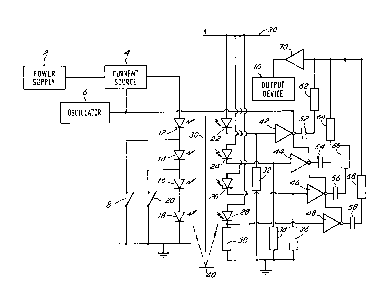
The detection circuitry shown in the 301e
~igure is arranged to be incorporated into a hand
drier for example to automatically energise a fan and
a heater when the presence of a hand is sensed in the
vicinity of the output of the drier. The fan and
heater are represented in the drawing by an output
device 10. The presence of a hand is sensed by an
array of transmitters co-operating with an array of
receivers.
The array of receivers are advantageously
shielded from direct line of sight with the
transmitter but respond to light from the
transmitters when reflected from the hand when
present. Instead the transmitter and receiver arrays
may be positioned in direct line of sight with each
other and arranged to respond when the light is
interrupted by the presence of a hand.
As shown in more detail the circuitry
includes a power supply 2 feeding a current source 4.
The current source 4 is gated by the output signals
from an oscillator 6 which may, for example, be in
square wave form having a mark space ratio of 1:10
and a frequency of 2 kHz. The frequency of 2 kHz is
selected in order that the subsequent receiving
circuits can filter out the dc content of sunlight
and the AC content of artificial light (fluorescent
lights operating at 50 or 60 Hz).
The current source 4 in turn feeds the
series combination of four light emitting diodes 12,
14, 16 and 18. A switch 20 is connected in parallel
with two series connected diodes 16 and 18 so as to
shunt these diodes out of circuit when not required.
1 31 3546
3426US
-- 5 --
A switch 8 is~ connected in parallel with the three
series connected diodes 14, 16 and 18 so as to shunt
these diodes out of circuit when not required. The
four diodes 12 to 18 de~ine a transmitter array.
A receiver array comprises four
photodiodes 22, 24, 26 and 28. ~ach photodiode 22 to
28 is connected in series with a respective one of
four resistors 32, 34, 36 and 38 and the four series
combinations are connected in parallel between a
l O positive supply rail 30 and earth.
The signal appearing out the junction
between the diode 22 and the resistor 32 is buffer
switched by an a buffer gating amplifier 42 fed
through a capacitor 52 forming a dc filter and
50-60 Hz AC filter through a resistor 62 to a summing
amplifier 70.
Similarly the signals appearing at the
juntions between diodes 24 to 28 and corresponding
capacitors 34 to 38 are buffer switched by respective
buffer gating amplifiers 44 to 48, filtered by
respective capacitors 54 to 58 and fed to the common
summing amplifier through respective resistors 64 to
68.
The output signal from the summing
amplifier 70 is fed to control the output device 10.
A shield 30 is provided between the
transmitter and receiver arrays and a reflective
surface 40 (such as a hand) is shown below the shield
by means of which light from the trasmitter array may
be directed at the receiver array.
The output of each buffer gating
amplifier 42 to 48 is connected to the oscillator so
that the buffer gated amplifiers 42 to 48 are
synchronously gated with the light tran~mitted by the
transmitter diode array.
1 31 3546
3426US
-- 6 --
The resistors 32 to 38 may be variable
resistors and are selected to provide a matched
impedance to their respective diodes.
In particular when the diodes 22 to 28 are
likely to be subjected to sunlight (direct or
indirect) the values of the resistors are selected so
that the diodes do not saturate and so mantain their
sensitivity to light from the transmitter array.
By using four light emitting diodes on the
transmitter array the sensitivity of each diode 22
to 28 is effectively increased by a factor of four.
This means that the detection range can be extended
without loss of sensitivity over the case when only
one transmitting diode is used.
Furthermore by using four photodiodes each
in an independant circuit and by AC decoupling and
then combining the four outputs in a summing
amplifier, the magnitude of the output signal is
increased by a factor of four without significantly
increasing the noise level, (noise being random tends
to averaged in the summing amplifier rather than
cumulative as with the detected signal). Also the
effects of saturation are avoided since the amplified
output signal is never allowed to approach the level
f the voltage on the positive rail 30 .
As a consequence the signal to noise ratio
is improved.
The detection circuitry described is a
multipurpose circuit which can be readily adapted to
cope with the different detection range requirements
in different environments. To reduce the range of
operations the switches 20 and 8 may be progressively
closed. Instead or in addition the outputs from the
amplifiers may be selectively inhibited by
~5 connections or circuitry (not shown). Of course, the
t3135~6
3426US
-- 7 --
number of light emitting diodes and photodiodes can
be increased or decreased at will.
It is a generalisation that the output
signal S from the summing amplifier is a function of
the number n of photodiodes in circuit and the number
m of light emitting diodes in circuit
ie, S = f (m.n)
where at least either m or n is a whole number
greater than one.
This is a significant advantage over the
prior art where, in order to increase the value of S
and to avoid saturation by sunlight, more expensive
components (photo transistors for example) and more
expensive amplifiers need to be used (in order to
avoid a low signal to noise ratio). The additional
cost of such components usually far exceeds the cost
of the increased member of cheaper components used in
the present embodiment.
~urthermore with the present embodiment the
effective operating range of the detector can be
increased virtually ad infinitum - something which is
not possible with the prior art arrangement.
The embodiment of the present invention
thus provides an unexpected result that by using
arrays of cheaper components and summing their
effects, better results can be achieved than by using
more expensive traditional arrangemen-ts where
sensitivity is usually finite.
The light transmitted and received is
preferably in the infra red range.
While a presently preferred embodiment of
the present invention has been illustrated and
described, modifications and variations thereof will
be apparent to those skilled in the art given the
teachings herein, and it is intended that all such
1 31 3546
3426US
-- 8 --
modifications and variations be encompassed within
the scope of the appended claims.