Note: Descriptions are shown in the official language in which they were submitted.
1313570
FIEL~ OF T~E INVEN~ION
The present invention relates to metallized
sensor/heater elements having improved physical and
chemical properties, and to their fabrication.
BACXGRO~ND OF ~EIE INV~TION
Silicon-based electronics systems have become
increasingly important in recent years, especially
for automotive applications. These silicon-based
electronics are used principally for storing control
algorithm~, process information and for directing
actuators to perform variou3 functions, including
steering, suspension and display of driver
information, to name but a few. While the design of
electronic~ ha~ advanced rapidly, the development o
sensor technology has not proceeded at the same rate,
and sensor designs continue to be based on dated
technologies which have inbred limitations. Silicon
has recently been identified as the basi~ for future
sensor technology, and this hopefully will close the
technology gap and permit greater application of
control systems utilizing sensor technology.
Silicon is now widely recognized in the industry
a3 being suitable for use in silicon-based
electronics, and silicon sensor designs can now be
created us~ng a variety of manuacturing processes,
one of the most promising of which is referred to as
"micromachining" which uses chemical proce~ses to
introduce three-dimensional mechanical tructure
into silicon. These "microstructure~", a~ they are
1 3 1 3570
referred to, can be made sensitive to specific
physical phenomena, such as acceleration, pressure
and fluid flow, so that it is possible to fabricate
accelerometers, pressure sensors and mass air flow
sensors (MAFS), including hot wire anenometers and
fuel flow rate detectors. Different aspects of
micromachining are reviewed in Lee et al, "Silicon
Micromachining Technology for Automotive
Applications", SAE Publication No. SP655, February
1986.
In order to improve the performance of such
devices, it is important for the heater/sensor
element to have a substantially constant and
preferably highly linear temperature coefficient of
resistance, which does not change with thermal
ageing. In the past, gold has been used as the
heater/sensor element but this has not met with
acceptance due to the fact that gold is not
compatible with most semiconductor processes, and has
a low resistivity, thereby requiring a long resistor
which uses valuable real estate on the silicon
wafer. Attempts have been made to improve the
metallization characteristics of gold when used in
conjunction with semiconductors by using a
chromium/gold metallization system, but this too has
proved unsuccessful because of interdiffusion
characteristics at temperatures higher than about
200C. Since mass air flow sensors are usually
operated at temperatures of at least 200C, the
material used for sensing and heating elements in
such sensors must have stable electric
characteristics under those heat conditions and, in
particular, must exhibit a stable thermal coefficient
` - 3 - 1313570
of resistance and sheet resistivity (R-sh).
SUMMARY OF THE INVENTION
It has now been found, according to the present
invention, that it is possible to fabricate metallized
sensor/heater elements having substantially constant and
linear temperature coefficient of resistance properties
and high sheet resistivity, while at the same time being
compatible with semiconductor processes used to fabricate
the elements.
Therefore, in accordance with the present invention
there is provided a metallized heater and sensor element
for flow sensors having a substantially linear temperature
coefficient of resistance of at least 2000 parts per
million/C, the element comprising a first metal layer of
a refractory metal, a second metal layer of a noble metal,
deposited on the first layer, and a substrate supporting
the first metal layer and conductor leads attached thereto.
In accordance with a second aspect of the present
invention there is provided a method for forming a
metallized heater and sensor element for flow sensors
having a substantially linear temperature coefficient of
resistance of at least 2000 parts per million/C
comprising the steps of depositing a first metal layer of
a refractory metal on a substrate, depositing a second
metal layer of a noble metal on the first metal layer, and
then attaching conductor leads to the second metal layer.
'
"-- 1 31 3570
In a preferred aspect, a metallization system is
employed which is selected from a metal system and a
silicide system each having a temperature coefficient of
resistance of at least 2000 parts per million/DC.
The temperature coefficient of resistance (hereinafter
TCR) of the metallized heater/sensor elements of the
invention is at least 2000 parts per million/C and can be
at least 3000 parts per million/C. Usually, the TCR is
2200 to 3500 parts per million/C preferably 2400 to 3200
parts per million/C. The TCR is substantially linear at
values of at least 2000 parts per million/~C when the
element is heated at elevated temperatures, typically at
least 200C, over an extended period of time, which may be
as short as 5 hours and as long as 100 hours. This is to
be contrasted with the TCR of the known chromium/gold
system which has an initial value at room temperature of
about 1800 parts per million/C and which drops
dramatically after about 5 hours of heating at about 350C
to around 350 parts per million/C or less (see Figure 3).
The metallization systems of the present invention can
be divided into two broad categories, namely those based
on metals per se and on metals per se in association with
metal-containing materials, such as metal oxides (referred
to herein as metal systems), and those based on metal
silicides (referred to herein as silicide systems).
The metal systems of the invention can comprise metals
and metal-containing compounds such as metal oxides.
Preferred metals are refractory metals, such
1 3 1 3570
as titanium, tungsten, molybdenum, hafnium, zirconium
and chromium, and noble metals, such as palladium and
platinum. It is particularly preferred to utilize
multiple layers of refractory and/or noble metals,
such a~ in the sensors mentloned above having first
and second metals. In those structures, the first
metal, which is typically in contact with a diaphragm
of a semi-conductor device such as a mass air flow
gensor, i3 preferably a refractory metal, such as
titanium, tungsten, molybdenum and hafnium, zirconium
and chromium, or combination3 of those metals, such
as titanium-tugsten, and the second metal is
typically a noble metal, such as gold and palladium.
Particularly good results have been obtained using
titanium-tungsten/gold. Good results have also been
obtained if a barrier layer is between the first and
second metal layers, with that barrier layer being
formed from a metal-containing material, such as a
metal oxide, or from another metal. Examples of such
metallization systemQ are chromium/oxide/gold and
chromium/nickel/gold layer systems. In such systems,
the barrier layer is the nickel layer or the oxide
layer. Particularly effective results have been
obtained u~ing the chromium/oxide/gold sy~tem in
which the oxide layer is dichromium trioxide.
Referring to the silicide systems, the silicide,
i.e. a compound of a metal and silicon, preferably
polysilicon, is formed by depositing poly~ilicon onto
a substrate followed by depositing the metal onto the
polysilicon and heating to form the silicide. Any
metal which form~ a silicide may be used, provided
the resulting silicided element exhibits the desired
stable electrical and physical properties noted
6 1 3 1 3570
earlier. The silicide is preferably selected from
platinum silicide, titanium silicide, molybdenum
silicide, tungsten silicide, cobalt silicide and
palladium qilicide. The most preferred silicide is
platinum silicide.
The metallization systems employed according to
the present invention exhibit numerous advantages
which make them highly desirable for use in
developing sensitive and accurate heater/sensor
elements. In particular, they ~xhibit TCR values of
~ 'B at least 2000 parts per million'Awhich are essentially
-'~ ' constant upon prolonged heating, i.e~ they vary no
more than about 1000 part~ per million~ ~referably no
more about 400 to 600 parts per millio~ when heated
for at least about 15 hours at at least about 250C.
In addition, good thermal stability and resistance to
thermal ageing are shown by the sensors metallized
according to the present invention, and high sheet
reqistivity is also exhibited, typically of the order
of 0.2 ohm/square to 5 ohm/square for metal systems
based on a metal thickness of 3000 Angstroms, and
about 2.0 to 2.5 ohm/square for silicide systems, for
example platinum ~ilicide, for a layer thicknes~ of
about 1000 Angstroms. This means that the sensor
elements can be made much shorter and thereby occupy
con~iderably less real estate on the silicon wafer.
Furthermore, sensors metallized according to the
present invention do not exhibi~ electromigration
problems and also have excellent corrosion resi~tance
and high melting point~. These advantages mean that
interdiffusion problems, ordinarily as~ociated with
chromium/gold layers, are significantly reduced in
the metallized sensors of the present invention. In
7 1 3 1 357~
light of this, while a barrier layer may be employed,
as noted earlier, it is not required to employ a
barrier layer to prevent interdiffu~ion occurring, a~
i9 invariably required when using chromium/gold
layers.
The stable temperature coefficient of resistance
properties and sheet resistivity exhibited by the
sensors metallized according to the present invention
are not shown by elements metallized using
chromium/gold layers (-~es Fi-gu~e~ . In addition,
with chromium/gold layers, it has been observed that
the sheet resistivity increases with increasing
temperature while the temperature coefficient of
re~istance decreases with increasing temperature.
This does not occur with ths metallized elements of
the present invention.
A further advantage arising from the present
invention is that the metallization can be carried
out at low temperatures, typically not higher than
500C, and more usually in the region of 350 to
400C. Thi 8 make~ the metallization process
compatible with emerging ~ilicon-ba~ed sen~or
technology whereby integrated ~ilicon sensors can be
processed without subjecting electronics already
present on the sensor to heat damage. The
metallization systems of the invention exhibit low
contact resistance, and thereby form good ohmic
contact, and exhibit particularly~good adhesion to
silicon or silicon dioxide present on a wafer.
BRIEF DESCRIPTION OF T~E DRAWINGS
8 1313570
The invention will now be described with
reference to the accompanying drawings, in which:
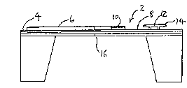
Figure 1 is a side view of a device including a
metallized element of the present invention;
Figure 2 is a plan view of the device of Figure
1 showing the configuration of the metallized element;
Figure 3 is a graph showing the effect of heat
treatment on the temperature coefficient of
resistance of chromium/gold;
Figure 4 is a graph showing the effect of heat
treatment on the temperature coefficient of
resistance of t$tanium-tungsten/gold;
Figure 5 i9 a graph showing the effect of heat
treatment on the temperature coefficient of
resistance of chromium/dichromium trioxide/gold; and
Figure 6 is a graph showing the effect of heat
treatment on the temperature coefficient of
resistance of chromium/nickel/gold.
DETAILED DESCRIPTION OE 1~ INVENTION
Referring to Figure 1, there is shown a
diaphragm structure, generally referenced 2, having
an area 4 containing integrated circuitry 6 and an
upper ~urfaco 8 supporting a heater element 10. While
the following description i8 in connection with the
element 10 comprising a metallization system of the
invention being a heater element a8 part of an
air-flow sensor, preferably a hot-wire anemometer, it
will be appreciated that the present invention i8
equally applicable to other senYor element-Y, such as
a bridge structure 12 and/or a cantiliver structure
14, shown schematically in Figure 1. The ma~s air
.,. ~ - ,
9 1313570
flow sensor shown in ~igure 1 comprises a diaphragm
portion 16 which i~ comprised of at least 2 layers,
one layer being typically of silicon dioxide and the
other typically being of silicon nitride. Preferably,
the portion 16 comprises three alternating layers of
silicon oxide, silicon nitride and silicon oxide. By
forming alternating layers of oxides and nitrides, it
is possible to offset the inherent compressive stre~s
exhibited by silicon oxide and the inherent ten~ile
stre~s exhibited by silicon nitride to produce a
laminated diaphragm layer with an overall low stres~.
Thi~ results in increased sensitivity and
flexibility, so that the mea~urement of the
speed/amount of a gas over the sensor can be
accurately effected. The diaphragm structure shown in
Figure~ 1 and 2 is formed by conventional back-side
etching techniques, such as are reviewed in the
above-mentioned paper to Lee et al, and so further
discus~ion here is believed to be unnece~sary.
Figure 3 shows the variation of the TCR for
Cr/Au a3 a function of time when heated at 350C. In
the graph, mean~ unannoaled Cr/Au, means annealed
at 200C., ~ means annealed at 250C., X means
annealed at 300C., 3 means annealed at 350C.,
and O means annealed at 400C.
As noted earlier, the metallization system
according to the present invention can comprise
either a metal ~y~tem or a silicide syqtem. Preferred
metal sy3tem~ are formed from refractory metals or
noble metals, as noted earlier, with the particularly
preferred metal system being titanium-tungsten/gold
(TiW/Au). According to a preferred embodiment, thi~
metal system is applied to the upper surface 8 of the
1313570
diaphragm by first depositing on the diaphragm a
layer of titanium-tungsten, in which the amount of
tung~ten is in excess of the amount of titanium.
Usually~ the tungsten i~ present in an amount of
about 90% by weight and the amount of titanium is
about 10% by weight. The titanium and the tungsten
are deposited using sputter deposition techniques in
vacuum at elevated temperatures, generally in the
region of 200 to 450C, usually about 250C. The
sputtering is continued until the thickness of the
layer of titanium-tungsten is about 200 to 2000,
preferably 500 to 1500, Angstroms, more usually about
1000 Angstroms. A layer of gold i~ then deposited on
top of the titanium-tungsten. Typically, the gold is
evaporated at about 350C from a graphite crucible in
vacuum. The evaporation of gold is continued until
the thickness of the gold layer is in the region of
2200 to 3500 Ansstroms, usually about 2400 Angstroms.
Etching of the metallization layer(s) is then carried
out using conventional technigues to form the desired
shaped heater/sensor element 10.
The TiW-Au metallization system has electrical
characteristics, such as TCR and R-sh, which are very
stable in the temperature range of about 25 to 400C.
In particular the TCR shows a high degree of
linearity over the temperature range of 25 to 400C
and over time period of 5 to 100 hours. Moreover, the
TCR at those temperatures and over those time periods
was above 2000 parts per million and ranged over
about 2700 to 3200 parts per million. This re~ult~ in
the TiW/Au system having a high TCR which is stable
when heated over extended time periods. sensitive.
Figure 4 of the present application shows the
11 1 31 3570
variation of the TCRs of TiW/Au over 20 hours of heat
treatment at 250C and 350C. It will be noted that
the TCR does not vary more than about 400 to 500
part~ per million over the 20 hour heating period.
The TiW/Au system did not exhibit interdiffusion
characteristics, which is principally due to the
lower self-diffusion coefficient for each of the
layers of TiW and Au. As a result of thi~,
electromigration characteristics were minimized,
thereby overcoming the problem~ experienced with
conventional chromium/gold ~ystems.
Another preferred metallization system is
chromium/oxide/gold. It ha~ been found that when the
oxide is dichromium trioxide, the metallization
~y~tem has a particularly stable and highly linear
TCR at 350C., as well as a stable R-sh. This is
shown in Figure 5, where it can be seen that the
varaition of the TCR over 20 hours of heating at
250C is no more than 600 parts per million, and is
more usually 400 to 500 parts per million. In the
graph, ~ means annealed at 250C. with no further
oxyger. treatment, ~ means annealed at 350C. with no
further oxygen treatment, a means annealed at 250C.
with oxygen treatment and means annealed at 350C
with oxygen treatment. Surprisingly, the dichromium
trioxide functions effectively as a barrier at 350C
even when present as an extremely thin oxide layer,
i.e. only 8 to 20 Angstroms, typically 12 to 15
Angstrom~, thick.
Th~ chromium/oxide/gold system i~ depo~ited on
the substrate by first depositing the chromium using
evaporation in vacuum at elevated temperature ,
usually in the region of 250 to 500C, more usually
12 1313570
about 350C. The dichromium trioxide is produced by
placing the substrate with the chromium layer so
formed into a furnace at about 800 to 1000C., and
introducing oxygen to oxidize a thin surface layer of
the chromium and form the chromium oxide. Finally,
the gold is deposited on the dichromium trioxide
layer using the evaporation techniques discussed
earlier in connection with the fabrication of TiW/Au
system~. Annealing is then preferably carried out
using a hydrogen-containing gas so as to reduce the
formation of any oxide on the surface of the
metallized element. Annealing is ordinarily carried
out for a period of about 20 to 120 minutes, usually
about 30 minutes at about 250 to 4~0C., typically
about 350C. The atmosphere is ordinarily nitrogen
gas containing about 4 to 8% by volume of hydrogen.
Another metallization system i~ the
chromium/nickel/gold sytem (hereinafter the Cr/Ni/Au
system). The varation of the TCR with temperature is
shown in Figure 6. This metallization system exhibits
stable and essentially linear TCR properties at 350C
over a significant period of time (20 hours). Good
R-sh propertie~ are also shown.
As noted earlier, the prior known chromium/gold
metallization system suffers from interdiffusion
characteristics giving rise to migration of chromium
and gold atoms into the other metal at the interface
of the two layers. As a result, the TCR drops
drastically upon prolonged heating, as shown in
Figure 3. In the Cr/Ni/Au system, the nickel
functions as a barrier layer between the chromium and
the gold, thereby minimizing electromigration and
interdiffusion problems.
13 1 31 3570
With reference to the silicide metallization
~ystems which may be employed according to the
invention, in principle any metal may be used which
will react with silicon, preferably polycrystalline
silicon or polysilicon, to form a silicide. A~ noted
earlier, numerou~ silicides may be employed, but the
mo~t preferred i~ platinum silicide. This material
has numerous advantages over gold which has been
widely used in the past. However, gold suffers from a
number of disadvantages, the principal ones being
that gold i~ not particularly compatible with mo~t
semiconductor processes, and gold has a low
resistivity, thereby requiring large re~istor
dimension~ which occupy valuable silicon area on the
wafer. Platinum ~ilicide, on the other hand, has a
sheet resistivity (R-sh) which is at least ten times
greater than the resistivity of an equally thick gold
layer. Thus, the ~ilicided sensor element can be made
much shorter and will thereby occupy considerably
les~ silicon area. Moreover, platinum silicide is
made from polysilicon which i8 widely utilized in the
fabrication of integrated circuits, and is therefore
compatible with the fabrication of sensor device~ on
the same silicon wafer. In addition, platinum
silicide is resistant to thermal stress, and can
withdstand temperatures in excess of 700C.
Furthermore, the TCR o platinum silicide is in the
range of about 2000 to 3000 parts per million, and
the TCR of platinum silicide is essentially constant
upon prolonged heating, which is highly advantageous
in developing flexible and sensitive sensors.
While platinum silicide is the preferred
~ilicide, other silicides have also been shown to
14 l 3 1 3570
exhibit excellent physical and chemical properties as
silicide metallization systçms for sensors,
particularly mass air flow sensors, pressure 3ensors
and accelerometers. Other silicides exhibiting these
excellent properties are titanium silicide, cobalt
silicide, molybdenum silicide, tungsten silicide and
palladium silicide. A~ a result of the excellent
physical and chemical properties of these materials,
it i9 possible to utilize such ~ilicide metallization
systems for contact to very shallow junctions (less
than 1000 Angstroms), for first level gate and
interconnect metals, and for heterostructures with
semiconducting silicides. Additional advantages
arising from the silicides of the invention is that
they can be deposited u~ing low temperature
techniques, typically at temperatures not higher than
500C, and more usually in the region of 350 to
450~C. Such processe~ include, for example,
sputtering, cosputtering, CVD (chemical vapor
deposition) proce~ses, sintering processes and the
like. The silicides employed in the invention have
low contact resistance and form good ohmic contact,
and show highly stable and essentially constant TCR
properties. The silicides also exhibit high
conductivity a3 well as excellent adhesion to silicon
or silicon dioxide. In addition, the silicides
exhibit excellent corrosion resi3tance, and do not
suffer from electromigration problemY.
The silicided element (for convenience of
description see element 10 in Figure l) is preferably
formed by depositing a layer of polysilicon on a
substrate, such a~ the diaphragm 16 shown in Figure 1
or a semiconductor silicon wafer, using conventional
13~3570
low pre~sure chemical vapor deposition. The
depo~ition i~ continued until the thickness of the
layer is in the region of about 3500 to 4500
Angstrom~, typically about 3800 Angstroms. A layer of
silicon oxide is then ormed on the polysilicon layer
under conventional wet oxidation condition3 u~ing
steam. The polysilicon is then patterned using
conventional photolithography technique~, followed by
reactive ion etching (RIE). A layer of the metal is
then depo~ited on the etched oxide/polysilicon layer.
In the case of platinum, deposition may be effected
by using electron beam (E-beam) or sputter deposition
at elevated temperature, for example 200 to 450C.,
typically at about 250C. The re~ulting platinum
layer has a thicXnes~ of about 800 to 2500 Angstrom~,
u3ually about 1000 to 2000 Angstroms. Sintering i3
then carried out at elevated tempera~ure, ordinarily
at about 350 to 600C., typically at about 550C.,
for a time period of about 10 to 35 minutes,
preferably about 15 minutes to form the silicided
element lO.
Anneal~ng may be carried out either by heating
to 350 to 500C under a nitrogen atmosphere, or by a
3tep-wise annealing proceedure wherein the wafer3 are
kept at about 350C under nitrogen for about one
hour, followed by increa~ing the temperature to about
450C for about an hour, followed by heating at about
550C for abour 30 minutes, and the cooling to about
350C before removing the furnace. The exces3
silicide i3 then etched using a cleaning ~olution,
such a~ aqua regia (nitric acid-l part/hydrochloric
acid-7 part~/water-8 part~), for about 10 to 45
seconds, usually about 15 seconds. The aqua regia may
16 1313~70
be heated to a temperature less than 100C., for
example about 85C. The continuity of the silicide
can then be checked using a parametric tester.
Particularly good re3ults are obtained from samples
with sputtered films and a long annealing sequence.
In addition, pre-sputtering to clean the sample
before actual deposition of the metal also improveq
the adhesion of the films to the polysilicon.
With particular reference to platinum, while
that metal may be evaporated at room temperature, it
is preferred to carry out the evaporation at elevated
temperatures, for example in the region of 200 to
300C, typically at about 250C. The most
advantageous deposition of platinum and subsequent
formation of platinum silicide is achieved by fir~t
cleaning the wafer u~ing the usual cleaning
materials, typically dipping the wafer into a
hydrogen fluoride ~olution for &bout 5 seconds and
then rinsing. The wafer is then cleaned by carrying
out a pre-sputtering step. Pre-sputtering is u~ually
carried out by "sputtering off" or cleaning the wafer
using argon ions. Following the pre-sputtering, the
platinum i8 deposited at a temperature of about 250C
until the layer is about a 1000 Angstroms thick.
Sintering is then effected at about 550C for about
minutes under a nitrogen flow, and this is
followed by sub~ecting the qintered material to an
aqua regia etch for about 15 seconds. Optionally,
titanium-tungsten/aluminum may be deposited on the
platinum silicide to further enhance the
metallization effect. It has been found that the use
of hydrogen fluoride following sintering i not
recommended as lifting of the metallized layer from
1 3 1 3570
17
the substrate may occur.
As noted earlier, the metallization systems of
the present invention not only exhibit stable and
essentially linear TCR properties, but also show high
sheet resistivity. The sheet resistivity for the
metal systems is usually in the range of 0.2 to 5.0
ohm/square for a metal layer thickness of 3000
Angstroms. The sheet resistivity for silicide
systems, e.g. platinum silicide, is generally in the
range of 2.5 ohm/square, more usually in the region
of about 2.2 to 2.3 ohm/square after sintering and
etching, based on a 1000 Angstroms thick layer of
platinum on top of polysilicon.
In order to obtain an accurate TCR measurement,
it is desirable to effect a minimum of three
resistance measurements. The third measurement is
designed to determine whether any permanent
resistance change has occurred as a result of the
temperature treatment. The TCR is defined as:
TCR = R - Ro
Ro x (T - To)
wherein R is the resistance at temperature T and Ro
is the resistance at temperature To.
The method of measuring TCR is well known to any
person of ordinary skill in the art. The techniques
and theory involved are reviewed in Buehler et al,
IEEE Transactions on Electron Devices, Vol. ED-33,
No. 10, page 1572 (1986). Van der Pauw resistor
structures according to the Buehler et al
18 1 3 1 3570
teaching were employed throughout the resiqtance
measurements at different tempera~ures.