Note: Descriptions are shown in the official language in which they were submitted.
1313~75
BACKGROUND OF THE INVENTION
Field of the Invention: The present invention relates
generally to the field of video amplifiers and more
particularly to wide band, high power video amplifiers,
which may be of the hybrid type, configured for
providing fast rise time output signals to video
displays.
Discussion of the Background: Video amplifiers are
used to provide high voltage, amplified signals to
video displays which typically present a relatively
high capacitive load to the amplifiers. Present video
amplifiers, having bandwidths of about 50 to 100 MHz,
typically provide output signals having voltages of
about 25 to 40 volts peak-to-peak, into loads of about
15 to 25 picofarads (pF). Under such conditions, the
rise times of the output signals provided by the video
amplifiers are typically in the range of about 4 to 8
nanoseconds.
Needs, however, presently exist for improved
video amplifiers which meet the performance
requirements of new generation, high resolution color,
1000 and 200Q line raster video displays, which have
come into demand in military graphics, air traffic
control displays and commercial CAD/CAM systems. These
new generation video displays ~ypically require
-2- 1313575
extremely fast amplified signal rise times of only
about 1 to 3 nanoseconds at 45 to 55 volts
peak-to-peak, when driving into loads of between about
4 pf to about 15 pF. Amplifiex bandwidths in excess of
about 100 ~Hz are also typically required by such new
generation displays.
The rise times of many currently available video
amplifiers are thus seen to be comparatively slow with
re~pect to the rise time re~lirements of new generation
displays and result primarily from the relatively high
capacitive load into which the amplifiers are required
to operate. These high capacitive loads are typically
comprised not only of the display capacitance but also,
for example, of the distributed wiring, interconnect
and circuit card capacitances, part-to-part capacitance
and other parasitic capacitances associated with the
electronic circuitrv in ~he amplifier output network.
It can be appreciated that with the comparatively
slow output signal rise times provided by typical,
presently available video amplifiers, very short
duration amplifier input signals, having pulse widths
equal to or less than the amplifier output signal rise
times, are "lost" and cannot be applied to the
associated display. Some signal information is
accordingly lost and the resolution of the associated
display is less than would be possible if the output
signal rise time were faster. Such loss of
short duration signals can adversely affect the
performance of the display equipment and is, in any
event, generally inconsistent with the requirements of
most high resolution video displays.
Most video amplifiers presently use conventional
solid state cascode amplifiers--that is, amplifiers
having a common emitter-common base pair of
transistors--as is more particularly discussed below in
the description of the present invention. Variations,
1 31 3575
known as frequency compensation circuits, have been
added to conventional cascode amplifiers to decrease
the rise and fall times associat~d therewith. For
example, the addition of a capacitance in the emitter
leg of the common emitter transistor of a cascode
amplifier, often called "emitter compensation," serves
to increase the high-frequency current generated in the
amplifier. When video pulses are amplified, this
technique serves to square off the output signal and
reduce the associated rise and fall times thereof.
Another such technique is the addition of output
inducatance in series and/or shunt with the load
capacitance.
There are, however, characteristic prcblems with
compensation circuits. For example, such circuits can,
while, improving the rise time, cause a ringing in the
output signal at turn on and turn off. Such signal
ringing manifests itself in the display as repetitive
"ghost" video (such as, for instance, dim vertical
streaks following a displayed vertical line), which
diminishes the sharpness of the video display and can
cause operator confusion when the display is crowded
with information. Consequently, additional circuitry is
often needed to reduce the ringing caused by the
compensation. As a result, wide bandwidth operation is
sometimes not achieved.
From the foregoing, it can be appreciated that
the development of new means for amplifier compensation
is needed, which, when either used alone or combined
with existing techniques, can achieve the high
amplifier speeds presently coming into demand in
today's new high resolution displays~ The invention
described herein implements a new such approach to
amplifier compensation.
1313575
SUMMARY OF THE INVENTION
A broadband, fast rise time and fall time, video
amplifier, according to the present invention,
comprises a main cascode amplifier having a video
signal input and an amplified video signal output, and
current boosting means coupled to the main cascode
amplifier. The current boosting means are configured
for causing, whenever the input video signal abruptly
changes in a first direction, a current spike to be
added to current across an output portion of the main
cascode amplifier in a manner causing the rise time of
the amplified video signal to be shorter than the rise
time which would otherwise be provided by the main
cascode amplifier in the absence of the current
boosting means. The current boosting means are further
configured for causing, whenever the input video signal
abruptly changes in a second, opposite direction, a
current spike to be subtracted from the current across
said main cascode amplifier output portion in a manner
causing the fall time of the amplified video signal to
be shorter than the fall time which would otherwise be
provided by the main cascode amplifier in the absence
of the current boosting means.
According to a preferred embodiment, the current
boosting means comprise first cascode boost amplifier
means for providing the current spike when the video
signal abruptly increases and second cascode boost
amplifier means for providing the current spike when
the video signal abruptly decreases. Inputs of the
first and second cascode boost amplifier means are
preferably capacitively coupled to the main cascode
amplifier so as to receive input video signals
therefrom.
Preferably, one of the first and second cascode
boost amplifier means comprise portions of the main
` 1 31 3575
cascode amplifier. Further, the current boosting means may
be configured for enabling the main cascode amplifier to
provide amplified video signals having a peak-to-peak
voltage of at least about 40 volts and having rise and fall
times of less than about 3.5 nanoseconds when the video
amplîfier i.s providing amplified video signals to a
capacitative load of at least about 25 pf, and to provide
rise and fall times of no more than about 1.8 nanoseconds
at a capacitive load of about 14.5 pf for about 20 volts
peak-to-peak.
Various aspects of the invention are as follows:
A broadband, fast rise time and fall time, video
amplifier which comprises: a) a main cascode amplifier
15 having a video signal input and an amplified video signal
output; and b) current boosting means coupled to said main
cascode amplifier for causing, whenever the video signal
abruptly changes in a first direction, a current spike to
be added to current across an output portion of the main
cascode amplifier in a manner causing the rise time of the
amplified video signal to be shorter than the rise time
which would otherwise be provided by the main cascode
amplifier in the absence of the current boosting means and
for causing, whenever the input video signal abruptly
changes in a second, opposite direction, a current spike to
be subtracted from the current across said main cascode
amplifier output portion in a manner causing the fall time
of the amplified video signal to be shorter than the fall
time which would otherwise be provided by the main cascode
amplifier in the absence of the current boosting means.
A broadband, fast rise time and fall time, video
amplifier which comprises: a) a main cascode amplifier
having a video signal input and an amplified video signal
output; and b) current boosting means electrically coupled
to said main cascode amplifier for causing, whenever the
video signal abruptly changes in a first direction, a
current spike to be added to current across an output
portion of the main cascode amplifier in a manner causing
the rise time of the amplified video signal to be shorter
1 31 3575
- 5a -
than the rise time which would otherwise be provided by the
main cascode amplifier in the absence of the current
boosting means and for causing, whenever the input video
signal abruptly changes in a second, opposite direction, a
current spike to be subtracted from the current across said
main cascode amplifier output portion in a manner causing
the fall time of the amplified video signal to be shorter
than the fall time which would otherwise be provided by the
main cascode amplifier in the absence of the current
boosting means, said current boosting means comprising
first cascode boost amplifier means for providing the
current spike when the video signal abruptly increases and
second cascode boost amplifier means for providing the
current spike when the video signal abruptly decreases,
inputs of said first and second cascode boost amplifiers
being capacitively coupled to the main cascode amplifier.
A broadband, fast rise time and fall time, video
amplifier which comprises: a) a main cascode amplifier
having a video signal input and an amplified video signal
output, said main cascode amplifier being configured for
providing amplified video signals having a peak-to-peak
voltage of at least about 40 volts; and b) current boosting
means coupled to said main cascode amplifier for causing,
whenever the input video signal abruptly decreases, a
current spike to be added to current across an output
portion of the main cascode amplifier in a manner causing
the rise time of the amplified video signal to be less than
about 3.S nanoseconds for an amplifier load of at least
about 25 pf and for causing, whenever the input video
signal abruptly increases, a current spike to be subtracted
from the current across said main cascode amplifier output
portion in a manner causing the fall time of the amplified
video signal to be less than about 3.5 nanoseconds for said
amplifier load.
BRIEF DESCRIPTION OF THE FIGURES
The present invention may more readily be understood
by a consideration of the accompanying drawings in which:
.. .. :
`` 1 3 1 3575
- 5b -
FIG. 1 is a circuit schematic drawing of a simplified
version of the high speed video amplifier of the present
invention showing the general configuration thereof;
FIG. 2 is a detailed circuit schematic drawing of an
exemplary implementation of the high speed video amplifier
of the present invention for particular application; and
FIG. 3 is a diagram depicting various voltage and
current signals associated with the amplifier of FIG 1:
FIG. 3(a) depicting a typical square wave voltage input
signal; FIG. 3(b) depicting a typical, uncompensated
voltage output signal; FIG. 3(c) depicting a voltage spike
signal applied to current boosting portions of the
amplifier of FIG. 1; FIG. 3(d) depicting a positive
current spike signal provided by a
1 31 3575
--6--
turn on current boosting portion of the amplifier of
FIG.l; FIG. 3(e) depicting a negative current spike
signal provided by a turn off current boosting portion
of the amplifier of FIG. 1, and FIG. 3(f) depicting a
compensated voltage output signal.
DESCRIPTION OF THE PREFERRED EMBODIMENT
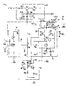
There is shown in FIG. l an exemplary circuit
diagram of a broad band, fast rise time, signal
inverting video amplifier 10 according to the present
invention. The circuit depicted in FIG. 1 represents a
simplified version of the more detailed circuit diagram
of FIG. 2, the simplified version (FIG. 1) being used
herein for purposes of describing and explaining the
invention so that the invention can be more readily
understood.
As depicted in FIG. 1, amplifier 10 comprises
generally a primary or main amplifier means 12 and
respective first and second current boosting circuits
or means 14 and 16. In turn comprising main amplifier
means 12 are a conventional input buffer 18 and a
conventional cascode amplifier 20. Input buffer 18, to
which a video signal, Vin (reference number 22), is
applied, comprises a complementary pair of NPN-PNP
transistors identified in FIG. 1 respectively as Q8 and
Q9 (80 as to be consistent with corresponding
transistor designations in FIG. 2). Emitters of
transistors Q8 and Q9 are connected together; the
collector of transistor Q8 is grounded and the
collector of transistor ~9 is connected to a negative
voltage source, for example, -15 volts. Input signal,
Vin, is applied to the bases of both transistors Q8 and
Q9. An internal signal, VIN' (reference number 24), is
provided, on a line 30, from the emitter junction of
1313575
--7--
transistors Q8 and Qs to a Point "A" internal to main
amplifier means 12.
Comprising cascode ampli~ier 20 are an NPN
transistor Ql and a pair of parallel connected, matched
NPN transistors Q5 and Q14. The use of the two
parallel connected transistors Q5 and Q14 is a matter
of choice to enable higher power operation than
generally would be possible with just one transistor.
However, as far as operation of cascode amplifier 20 is
concerned, the two transistors Q5 and Q14 function as a
single, common base NPN transistor. As shown in
FIG. 1, the internal signal, VIN', on line 30 is fed to
the base of transistor Q1 through a base resistor, RBl.
The emitter of transistor Ql is connected, through an
emitter resistor, ~ 1' to -VEE by a conduit 32. The
collectors of transistors Q5 and Q14 are connected,
through a load resistor, RLoAD, to a positive voltage,
for example, +65 volts, on a line 34, and the bases of
such transistors are grounded. A V0uT line 36 is
connected, at a Point "D," between load resistor,
RLoAD, and the collectors of transistors Q5 and Q14.
A capacitor, designated in FIG. 1 as CTOTAL, is
depicted as being connected between V0uT line 36 and
ground. It is to be understood, however, that
capacitor CT0TAL represents the entire capacitance
"seen" by amplifier 10, thereby including not only the
normal load capacitance of whatever equipment may be
connected for receiving the V0uT signal, but other,
internal capacitances as well.
From the foregoing description, it can be
appreciated that amplifier means 12 are similar to a
conventional, cascode-type video signal amplifier.
Such a conventional cascode amplifier would, in the
absence of first and second current boosting means 14
and 16 of the present invention, typically provid~ a
rounded off, amplified output voltage waveform of the
1 31 ~575
--8--
general shape depicted in FIG. 3(b) and identified by
reference number 40. Such output signal 40, which has
relatively slow rise and fall times (as conventionally
defined using the 10 percent and 90 percent points of
the waveform) is generally improved by the addition of
first and second inductors, L1 and L2, in respective
lines 34 and 36, as shown in FIG. 1. Resistors R1 and
R2 (shown in phantom lines in FIG. 1) may be added in
shunt with respective inductors L1 and L2 to reduce
ringing caused by the inductors and provide additional
output signal improvement. Such inductors, L1 and L2,
and shunt resistors, R1 and R2, may advantageously be
incorporated in amplifier 10 as shown.
Amplified video output signal, VOuT, can,
however, still be substantially improved, and the
associated rise and fall times correspondingly
decreased, as depicted by waveform 42 in FIGS. 1 and
3(f), by the incorporation of first and second current
boosting circuits 14 and 16 (FIG. 1) described
hereinbelow.
Referring to FIG. 1, first current boosting
circuit 14 is seen to comprise a second cascode
amplifier having two PNP transistors Q3 and Q4, the
collector of transistor Q3 being connected to the
emitter of transistor Q4. The emitter of transistor Q3
is connected, through a resistor RE3, to a positive
voltage, for example, +70 volts. The base of
transistor Q3 is connected, through a base capacitor,
CB~, to Point "A" of main amplifier means 12 (via a
line 44) so as to receive internal voltage signal VIN'.
A resistor, RD3, is connected from a Point "B" at the
base of transistor Q3 to the +70 volt supply. A base
resistor, RB3, is connected from Point "B" to the base
of transistor Q4. The collector of transistor Q4 is
connected, via a line 46, to Point "D" in line 34
located between the collectors of transistors Q5 and
-
9 1313575
Q14 and inductor Ll. The output of first current
boosting amplifier circuit 14 is provided, over a line
46, to the output of cascode amplifier 20.
Second current boosting circuit 16 comprises an
NPN transistor Q2, the base of which is grounded
through a base resistor, RB2, and is connected by a
line 50, through a capacitor, CB2, to Point "A" (at
which VIN' is provided). The emitter of transistor Q2
is connected to a negative voltage, for example, -15
volts, through an emitter resistor, ~2. A Point "c"
at the base of transistor Q2 is connected through a
resistor, RD2, to the -15 volt source. The collector
of transistor Q2 is connected, via a line 52, to a
Point "E" located between the collector of transistor
Ql and the emitters of transistors Q5 and Q14. In
this latter regard, second current boosting amplifier
circuit 16 is considered also to include the pair of
transistors Q5 and Q14 as the other portion of what is,
therefore, a third cascode amplifier.
Operation of Current Boostin~_Circuits 14 and 16 From
FIG. 1 it can be seen that the VIN' signal provided
internally at Point "A" provides at first current
boosting circuit Point "B," through capacitor ~B3' and
at second current boosting circuit Point "C," through
capacitor CB2, a sharp negative-going voltage spike at
the leading edge of the VIN' signal and a sharp
positive-going voltage spike at the trailing edge of
the VIN' signal. A resulting voltage spike signal 60,
depicted in FIGS. 1 and 3(c), is thus provided at both
Points "B" and "C" by VIN -
The negative-going voltage spike of signal 60 at
Point "B" of first current boosting amplifier circuit
14 drives the second cascode amplifier on for an
instant, thereby causing a positive-going current spike
1 3 1 3 57 5
--10--
62, FIGS. 1 and 3(d), to be output to Point "D"
associated with cascode amplifier 20 at the instant of
VOUT turn on. The positive-going voltage spike at
Point "B" has no operational effect on first current
boosting amplifier circuit 14 (except as mentioned
below). In a similar manner, the positive-going
voltage spike of signal 60 at Point "C" of second
current boosting amplifier circuit 16 drives the third
cascode amplifier on for an instant, thereby causing a
negative-going current spike 64, FIG.s 1 and 3(e), to
be output to Point ~E~' of first cascode amplifier 20 at
the instant of VOuT turn off. The negative-going
voltage spike at Point "C" has no operational effect on
second current boosting current amplifier circuit 16
(except as mentioned below).
Positive-going current spike 62 at Point "D"
associated with cascode amplifier 20 sharpens the
amplifier rise time and negative-going current spike 64
at Point "E" sharpens the amplifier fall time.
By way of illustrative example, coupling
capacitors CB2 and CB3 associated respectively with
first and second current boosting amplifier circuits 14
and 16 are indicated on FIG. l as having values of 33
pf. Other components shown in such FIG. are not,
however, identified as to either type or value since
FIG. 1 represents a simplified version of FIG. 2, on
which part types or values are indicated.
FIG. 2 thus shows in electrical schematic form an
exemplary implementation of above-described amplifier
10 which may advantageously be constructed in hybrid
electronic form. For reference purposes, the above
-described Points "A" through "E" shown in FIG. 1 are
identified in FIG. 2. Likewise, the transistor "Q"
designations used in FIG.s l and 2 are the same. The
circuit depicted in FIG. 2 is considered to be self
explanatory to those skilled in the electronics art and
1 3 1 3575
--11--
no useful purpose will be served by a detailed
description of such circuit. It is, however, noted
that a typical output load is identified in FI~. 2 by
reference number 70.
By way of a continued specific example, to which
the present invention is not limited, it has been
determined that the amplifier circuit depicted in
FIG. 2 has capabilities for providing output signal,
V0uT, rise and fall times of no more than about 3.5
nanoseconds, for a peak-to-peak output signal of about
40 volts, driving a load of at least about 25 pf. Such
circuit has also been demonstrated to provide output
signal rise and fall times of only about 1.8
nanoseconds driving into a load of about 14.5 pf for
about a 20 volt peak-to-peak output signal, and is
expected to provide such turn on and turn off times for
a 40 volt peak-to-peak output signal.
It is to be appreciated that first current
boosting amplifiex 14 can alternatively be biased so
that, in addition, a negative-going current spike is
provided when the input video signal goes positive
and/or second current boosting amplifier 16 can
alternatively be biased so that, in addition a
positive-going current spike is provided when the input
video signal goes negative. In such case or cases, the
positive current spikes add together and the negative
current spikes add together.
Amplifier 10, as depicted in FIGS. 1 and 2 and as
described above, is a signal inverting amplifier, as is
typical of cascode amplifiers. This signal inverting
configuration requires (as described) first current
boosting amplifier 14 to provide positive current spike
62 to Point "D" when the input ~ideo signal is
negative-going and requires second current boosting
amplifier 16 to provide negative current spike 64 to
Point "E" when the input video signal is
1 31 3575
-12-
positive-going. It is, however, within the scope of
the invention to modify amplifier lo, for example, by
the addition of signal inverters, so that it is
non-signal inverting. In such case, first current
boosting amplifier 14 would provide positive current
spike 62 to Point "D" in response to the input video
signal going positive (instead of negative) and second
current boosting amplifier 16 would provide negative
current spike 64 to Point "E" in response to the input
video signal going negative (instead of positive~.
Although there has been described herein a
particular embodiment of a high speed, broad band video
amplifier in accordance with the present invention for
the purpose of illustrating the manner in which the
invention may be used to advantage, it is to be
understood that the invention is not so limited.
Accordingly, any and all variations or modifications
which may occur to those skilled in the art are to be
considered to be within the scope and spirit of the
invention as defined in the appended claims.