Note: Descriptions are shown in the official language in which they were submitted.
~ 3 ~
This invention relates to a film forming apparatus
for forming a film such as an epitaxial layer on objects
to be coated with a film such as wafers.
With the trend toward higher integration and
progressive microminimization of IC's, it is becoming a
widespread practice to grow epitaxial crystals on semi-
conductor substrates (hereinafter referred to as wafers)
for ~10S devices, for example. As the wafers increase in
diameter, the epitaxial layer is becoming gradually
thinner.
The reaction apparatuses for epitaxial growth are
broken down into three types: the horizontal reaction
tube system, the vertical bell jar system and the barrel
system. The latest addition is the recently-developed
hot wall type, a modified version of the low pressure
CVD system. The constructional outline of these reac-
tion apparatuses is that a holder (hereinafter referred
to as a susceptor) for holding wafers is placed in a
high-temperature reaction furnace and reactive gases
such as silicon tetrachloride (SiCQ4) and silane are
introduced into the reaction furnace.
In forming an epitaxial film, it is important to
keep uniform the thic~ness and the electric resistance
of the film in order to secure high quality. With any
of the above-mentioned reaction apparatuses, however,
it is impossible to control temperature in an epitaxial
process to produce uniform temperatures for all the
~3~
-- 2 --
wafers and for the different positions of each wafer
where chips are formed. As a result, the temperature
distribution becomes non-uniform.
The temperature distribution of the wafers is
determined according to a balance between the heat
given by conduction and radiation from the susceptor and
the heat loss by radiation from the surfaces of the
wafers.
Normally, the reason for the irregular te~perature
distribution is that since the heat losses differ among
the wafers and also at the different positions of each
wafer even if the wafers are heated uniformly by the
susceptor.
In some reaction furnaces of bell jar system, a
metal coating is formed on the outer surface to pro-
vide radiation heat so that the heat is distributed more
uniformly, but the quantity of radiation heat from the
metal coating decreases with the growth of an epitaxial
layer, resulting in the temperature distribution
becoming uneven. The metal coating deteriorates as the
epitaxial process is repeated. In addition, the tem-
perature distribution is made uneven by the inflow rate
of a reactive fluid.
As set forth above, the conventional apparatuses
have a drawback that the temperature distribution as
well as the fluid flow is uneven, making it impossible
to secure a uniform thickness and a uniform electric
~31L~3:L~
resistance for the epitaxial film.
If one wishes to form a film on a number o~ wafers
at the same time, he has to use a large-size apparatus,
which makes the temperature distribution even ~ore irre-
gular.
The object of this invention is to provide a film
forming apparatus capable of forming a film on a number
of objects in one process in a manner that the thickness
and the resistance are uniform among the separate films
and over the whole area of each film.
This invention can be more fully understood from
the following detailed description when taken in con-
junction with the accompanying drawings, in which:
Fig. 1 is a diagrammatic perspective view partly in
section of a film forming apparatus according to a first
embodiment of this invention;
Fig. 2 is a diagrammatic sectional view of a film
forming apparatus according to a second embodiment of
this invention;
Fig. 3 is a diagrammatic sectional view of a
film forming apparatus according to a third embodiment;
and
F~ig. 4 is a partial sectional view of a modified
example of wafer support means.
With reference to the accompanying drawings,
description will now be made of film forming apparatuses
according to the preferred embodiments of this invention,
which epitaxially grow single-crystal silicon layers on
silicon wa~ers whose surfaces have been finished in a
mirror finish.
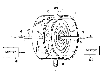
Referring to Fig. 1 showing a first embodiment of
this invention, numeral 1 indicates a cylindri~al
reaction f~lrnace having both its ends closed. The reac~
tion furnace has a reaction chamber formed in it.
Reaction furnace 1 is formed of a heat-resistant member
such as quartz glass and a metal. The shape of this
reaction furnace is not limited to a circular form, but
may be elliptical or rectangular. Reaction furnace 1
may be cooled in operation by conducting cooling water
through its walls. Injection nozzles 2, 3 and 4 are
provided at the top center of the peripheral surface and
at the centers of both sides of reaction furnace 1,
respectively. These injected ports are connected to
supply sources of gaseous reactive fluids such as sili~
con tetrachloride (SiC~4) and silane. The reactive
fluids are supplied from these supply sources into the
reaction chamber. Discharge nozzle 5 is provided at the
bottom o~ the peripheral surface of reaction furnace lo
; This discharge nozzle 5 is connected to a vacuum pump
and a surplus fluid in the chamber is discharged from
this discharge nozzle 5. The positions of the injeetion
and discharge nozzles are not limited as described above.
For example the injection and discharge nozzles may be
respectively provided at the bottom and top portions of
~3~3~
the furnace.
In this reaction chamber, there are provided a pair
of disc-shaped holders or susceptors 7 and 8, located in
almost vertical position and coaxially and opposed a
specified distance apart. These susceptors are made of
a heat-resistant material such as carbon. The suscep-
tors have a number of circular depressions formed on
their opposing sides. The circular depression~ are
arranged at specified intervals along a circle having
its center at the center of each susceptor. The circle
need not be one as in this embodiment, but may be
plural. The depressions should preferably ba arranged
uniformly in radial direction from the center of each
susceptor.
The individual depressions should have the same
diameter which is a little larger than that of silicon
wafers 6 to be inserted thereina Susceptors 7 and 8 are
fixed respectively to one end each of hollow rotating
shafts 9 and 10 extending coaxially. The other ends of
rotating shafts g and 10 protrude outward through the
side walls of reaction furnace 1 and rotatably supported
by the side walls through bearings attached thereto.
In this embodiment, the above-mentioned injection
nozzles 3 and 4, inserted into shafts 9 and 10, are com-
posed of tubes which are open between the susceptors inthe reaction chamber. The above-mentioned shafts 9 and
10 are connected respectively to first and second motors
~3~3~
tll and ~12 and are rotated by these motors mutually in
opposite directions. As a result, first susceptor 7 and
second susceptor 8 rotate in the opposite directions.
~leanwhile, driving means to rotate the susceptors
in the opposite directions may be composed o~ a motor
and a transmission device to transmit two, normal and
backward torques derived from this motor.
High frequency coils are at~ached to the sides of
the above-mentioned susceptors 7 and 8 which are oppo-
site to their sides ~acing each other. These coils areconnected electrically to an external power source
through known means such as slide contacts to enable
electric power from a power source, not shown, which is
located outside, to be supplied to the susceptors even
lS when the susceptors are rotating.
The operation of a film forming apparatus
constructed as described above will now be described in
the following.
As illustrated, mirror-finished wafers 6 are placed
in the depressions of susceptors 7 and 8 and held firmly
therein by support means, not shown. To take examples,
the holding means may be one which comprises a projected
edge at the periphery of the depresslon which will be
described later with reference to Fig. 3 or anather
means which is capable of setting desired diameters for
the outer periphery of the wafer and the inner periphery
of the depression to ensure a tight contact between
them.
Then, while susceptors 7 and 8 are rotated mutually
in opposite directions by driving motors Ml and M2, high
frequency coil 11 is energized. The reactive fluid C is
introduced into the reaction chamber through injection
nozzles 2, 3 and ~ and the unnecessary gas in the
chamber is discharged from discharge nozzle 5. Thus, an
epitaxial layer is formed on the surfaces of wafers 6 by
the reactive fluid.
~ith the film forming apparatus constructed as
described, while the wafers to be coated with a film
are held by a pair of susceptors, epitaxial layers are
formed on the wafers~ Therefore, it is possible to
deposit a film on a number of wafers in one process,
obviating the need to make a large-size apparatus. The
wafers are located opposed by a pair of susceptors 7 and
a and the opposing wafers are rotated changing their
relative position. Hence, the mirror-finish facas of
the wafers 6 reflect the radiation heat toward the
wafers on the opposite side. In other words, the
opposed wafers serve as the radiation heat sources with
the result that the temperature distribution between the
opposed wafers is made uniform with better efficiency.
The relative movements of susceptors 7 and 8
ensures a uniform temperature distribution over the
whole areas of the susceptors. Therefore, the tem-
perature distribution and the flow of the reactive fluid
:~ 3 ~
of not only over each wafer but of all wafers are made
uniform. Consequently, the conditions of epitaxial
reactions become identical for the surfaces of all
wafers, thereby producing epitaxial films with uniform
thickness and uniform resistance.
With reference to Figs. 2 and 3, description will
now be made of second and third embodiments. In these
embodiments, the same numerals are used for those parts
virtually identical to those in the first embodiment and
their description will be omitted.
In the second embodiment as shown in Fig. 2,
susceptors 7 and 8 are provided tilted a little so that
their portions located at the lower positions come
closer, with the result that the bottom faces of the
depressions are tilted a little from a vertical plane.
Thus, the wafers 6 in the depressions are prevented from
dropping therefrom. Depressions 12 for holding wafers,
provided in the susceptors, have the inside diameter a
little larger than the outside diameter of wafers 6.
If the inside diameter of depressions 12 is too large
in relation ~o the outer diameter of wafers 6, the
depressions' function to hold wafers is reduced. Hence,
the former should preferably b0 less than 1.1 times
larger than the latter.
If the inside diameter of the depressions is larger
than this, there is a possibility that the wafer rota-
tion in the depressions which occurs as the susceptors
3 ~
rotate beco~es irregular, resultiny in non-uniform rota
tion of the wafers. High frequency coils 11 are located
a specified distance away and facing the sides of
susceptors 7 and 8 which are opposite to the sides wnere
the depressions are formed. Those coils 11 are fixed
in reaction furnace 1 and rotating shafts 9 and 10 of
susceptors 7 and 8 are inserted rotatably in the central
portions of coils 11. Theref-ore, coils 11 are not
rotated by the rotation of rotating shafts 9 and 10.
In the apparatus constructed as shown in Fig. 2,
the wafers put in the depressions 12 of susceptors 7 and
8 do not fall out of the susceptors in an epitaxial pro-
cess even if any special members are attached. When the
susceptors rotate, the wafers rotate or make a toroidal
lS motion as they revolve around the rotating shafts.
Therefore, no local irregularity in temperature distri-
bution occurs for the wafers. The space between suscep-
tors 7 and 8 becomes narrower toward the bottom.
Consequently, the reactive fluid flowing in the s~ace
increases in flow velocity as it flows downward and the
dirt adhering to the susceptors is removed by the fluid
flowing at high velocity and discharged from discharge
nozzle 5.
In the third embodiment of Fig. 3, there are pro-
vided two pairs of susceptors 7 and 8 in reaction fur-
nace 1. As in the above-described embodiment, connected
to the members at the inside and outside of each pair of
-- 10 --
susceptors are rotating shafts 9 and lO having gas supply
tube coaxially inserted therein.
In this embodiment, the susceptors located inside
are fixed by a Eixed shaft and cannot rotate. As a
result, only the susceptors located outside rotate in
an epitaxial process. In this case, rotating shafts 9
and 10 may be rotated either in the same direction or in
opposite directions.
~n addition, it is also possible to rotate suscep-
tors 7 and 8 in mutually opposite directions as in theabove embodiments by using a rotating shaft in place of
fixed shaft 13 and rotating the rotating sha~t through a
bevel gear or the like by means of a rotating shaft
inserted at right angles with the above-mentioned rotat-
ing shafts 9 and lO into reaction furnace l. Susceptors7 and 8 are provided in vertical position and depres-
sions 12 for holding wafers, formed on one side each of
the susceptors, have their bottom faces tilted. Thus,
the wafers can be prevented from alling out of the
susceptors just as the susceptors being tilted in the
second embodiment, Injection nozzle 2 has two separate
branches 2a, each one of which is located just above
between a pair of susceptors 7 and 8. Each one of two
discharge nozzles 5 is located just below between a pair
of susceptors 7 and 8.
With the apparatus according to the third embodi-
ment of this invention, it is possible to form epitaxial
13~
layers on wafers in greater numbers in one process~
In the second and third embodiments of this inven-
tion, the wafers are seated a little tilted from a
vertical plane to hold the wafers on the susceptors.
However, as shown in Fig. 4, projected edge 8a may be
formed at the periphery oE each depression of susceptors
8 to hold the peripheral edge o~ wafer 6. Such a pro-
jected edge may be used in combination with a technique
for tilting a wafer,
This invention is not limited to the above-
described embodiments. For example, this invention may
be applied to CVD processes other than the epitaxial
process. The wafers used need not be confined to those
of silicon but may be formed oE other materials such as
compound semiconductors. A pair of susceptors may be
rotated in mutually opposite directions or one of the
susceptors may be rotated. Also, the susceptors may be
rotated at mutually different velocities. Put other-
wise, it is only necessary to rotate the susceptors
changing their relative position.