Note: Descriptions are shown in the official language in which they were submitted.
13141~
,
OPI'ICAL CONNECTOR
Back~round of the Invention
This invention relates to optical fiber connectors.
Due to the increasing need for higher capacity data and voice
5 transmission, use of optical fiber arrays is becoming necessary in many
applications. Alignment of such fiber arrays either with other arrays or with
optical components is troublesome, especially for the case of single mode fiberswhich have an extremely small core diameter (typically app~oximately 8 ~lm).
A typical connector for fiber arrays comprises two plugs of silicon
10 with grooves formed therein for accommodating the fibers. Each plug is formedfrom two mated members which are bonded together to encase the fibers. The
grooves are formed prior to bonding by anisotropically etching a major surface of
each member in an array corresponding to the fibers so that when the members arebonded, each fiber lies in a groove which is precisely aligned with all other fibers
15 in the array.
While the fibers within a plug may be fairly closely aligned with each
other, a problem exists in aligning these fibers with another fiber array or with an
array of optical components. One technique employs a precise thickness of each
plug and a precise lapping of the edges of each plug for alignment of different
20 plugs, aided by four springs, each contacting one of the major surfaces of the
aligned plugs (see, e.g., U.S. Patent No. 4,725,120 issued to Parzygnat). While
effective in aligning the plugs, such precise machining of the plug surfaces is
expensive. Another approach employs etching of deep grooves in the top and
bottom surfaces of each plug and then aligning the two plugs by means of a chip
25 extending between the two plugs and having ridges which fit within the grooves.
(See, e.g., U.S. Patent No. 3,864,018 issued to Miller). Again, precise machining
of the plug surfaces is expensive. A still further approach employs grooves which
are machined on the edges of the plugs and utilizes alignment pins pressed into
the grooves by spring clips to bridge the gap between plugs (see, C. M. Miller,
"Optical Fiber Splices and Connectors", pp. 336-338). Again, the alignment "
grooves have to be precisely machined with respect to the fiber grooves and thisadds considerable expense to the connector.
An alternative approach is to form deeper alignment grooves in the
same surfaces of the silicon members and at the same time as the fiber grooves.
35 Guiding rods are pressed into the alignment grooves by spring plates and span the
gap between plugs to provide the alignment (see, e.g., U.S. Patent No. 4,279,468
131~61
- 2 -
issued to Turley).
It is, therefore, an object of the invention to provide a connector for
optical fibers which will produce close alignment of the fibers with other fibers or
optical components.
S Summary of the Invention
This and other objects are achieved in accordance with the invention,
which in one aspect, is an optical fiber connector. The connector comprises a
block of material with edge and major surfaces. The block includes at least one
groove with sloping sidewalls formed in a major surface and adapted to receive an
10 optical fiber. The block also includes a beveled portion extending from the major
surface on each edge surface such that the slope of each beveled portion is the
same as one of the sidewalls of the groove. A spline is disposed in contact withthe beveled portion of at least one edge surface, extends beyond the plug, and is
adapted for engagement with the beveled portion of a similar plug for alignment
lS therewith. Means are also included for maintaining the spline in contact with the
beveled portion.
In accordance with another aspect, the invention is a method of
forming an optical fiber connector from a block material having major surfaces.
A f~rst groove is formed in a major surface of the block and is adapted for
20 receiving an optical fiber therein. A pair of grooves is also formed in the major
surface, one on either side of the first groove and essentially parallel therewith.
The pair of grooves are deeper than the first groove and are formed essentially
simultaneously with the first groove. The block of material is cut through a
bottom portion of the pair of grooves and along a line essentially parallel with the
25 first groove thereby forming edge surfaces including beveled portions extending
from the major surface of the block which includes the first groove.
Brief Description of the Drawin~
These and other features of the invention are delineated in detail in
the following description. In the drawing:
FIG. 1 is an exploded perspective view of a connector in accordance
with one embodiment of the invention;
FIG. 2 is an end view of a portion of the connector of FIG. I;
FIG. 3 is a cross-sectional view of a portion of the connector during a
stage of fabrication in accordance with an embodiment of the method of the
35 invention; and
131~
- 3 -
FIG. 4 is an exploded perspective view of a connector in accordance
with a further embodiment of the invention.
It will be appreciated that for purposes of illustration, these figures are
not necessarily drawn to scale.
5 Detailed Description
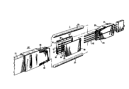
One form of the connector is illustrated in the exploded perspective
view of FIG. 1 and the end view of FIG. 2. Each half connector (plug), e.g., 1,
includes two blocks 10 and 11, of a material with facing major surfaces 12 and
13, respectively. The plugs are desirably made from a crystal material such as
10 silicon, for reasons which will become clearer. Each major surface has an array
of grooves, e.g., 14 and 15, etched therein. The grooves are of a size and shapeso that when the two blocks are bonded together, corresponding grooves in each
surface will accommodate an optical fiber, e.g., 16, from an array of fibers to be
connected (see FIG. 2). Each fiber will make contact with the sloped surfaces of15 the two corresponding grooves from the blocks as shown.
Use of a crystal for the block material permits taking advantage of
certain crystal planes to precisely forrn the groove surfaces. For exarnple, a
silicon block with a major surface in the (100) crystaDographic plane will be
etched anisotropically to forrn grooves with surfaces Iying in the (111) planes.20 Therefore, the angle of the two sloping walls of a groove will always be precisely
determined by the orientation of the crystal planes (in this example, approximately
55 ) with respect to the major structure regardless of the time of etching the major
surface. The size of the opening will therefore primarily be determined by the
size of the openings in the etch mask. Even if some overetching or underetching
25 of the grooves should occur, the angles of the groove walls will remain the same
and the position of each fiber will shift with respect to the major surface of the
block by the same amount. Thus, the fibers will always be rectilinear.
It will be appreciated that while the grooves are shown with a "V"
conSguration, it is also possible to achieve grooves with a flat bottom by stopping
30 the etching short of a complete etching of the crystal planes. However, sloping
sidewalls with the same orientation will still be produced.
While the fibers in each plug are closely aligned with each other,
mating such a member with the other plug of the connector of the same
construction (30 of FIG. I) to make the connection to another fiber array (within
35 fiber ribbon 21) presents a serious problem. This is due to the fact that thegrooves of the blocks making up the other pJug, 30, may not have been etched to
131~161
- 4 -
precisely the same extent as those of the plug 1. Hence, the two fiber arrays may
be shifted with respect to their respective block surfaces and therefore misaligned.
This problem is especially acute when the fibers are single mode fibers since they
have an extremely small core diameter (typically 8 ,um).
In accordance with a main feature of the invention, alignment between
the fiber arrays is provided by forming beveled portions (17, 18, 19 and 20) on
each edge surface of each block 10 and 11 (the beveled surfaces are similarly
formed on the blocks of plug 30). The beveled portions extend from the major
surfaces (12 and 13) of each block and have the same slope as the groove
10 surfaces.
Such beveled portions can be formed as illustrated in FIG. 3. Each
block, such as 10, is formed from a larger silicon wafer 40. A standard mask
material, 41, such as therrnally grown SiO2 deposited over the major surface of
the wafer which is the (100) crystallographic plane. The mask openings are
15 formed by standard photolithographic techniques to expose the areas of silicon
where the fiber grooves will be etched. Wider mask openings are also formed
over the silicon areas adjacent to the fiber grooves (one on each side of the array).
Typically, the openings for etching the fiber grooves are approximately 140 llm
wide, while the openings for etching the larger grooves are approximately
20 1000 llm wide. A standard anisotropic etchant is then applied to the structure to
form the fiber grooves (e.g., 14) and deeper grooves 21 and 22 adjacent thereto.The deeper grooves include side walls, e.g., 18 and 20, which have the same slope
as the fiber grooves since they are formed by the same anisotropic etch along the
same crystal planes (the (111) plane). The fiber grooves would be typically
25 approximately 98 llm deep while the adjacent grooves (21 and 22) would be
approximately 500 llm deep.
With certain etchants, such as ethylene diarnine pyrocatechol (EDP), it
is possible to etch both sets of grooves in a single step, since no significant
undercutting of the mask is produced for the fiber grooves while the deeper
30 grooves are being etched. An etchant which tends to undercut the mask, such as
KOH can still be used in a single step if the mask openings over the fiber groove
area are made sufficiently narrow to take this undercutting into account.
Alternatively, the two sets of grooves can be formed in two etching steps. For the
first step, mask openings would be formed only over the area of the deeper
35 grooves and those areas would be etched to a predetermined depth short of thedesired depth for those grooves. Openings in the mask would be made over the
~3141~1
area comprising the fiber grooves, and these fiber grooves would then be etched to
their desired depth while the etching of the deeper grooves would be completed.
After the etching of the grooves, the mask is stripped off. The wafer
is then cut into individual blocks by sawing through the etched surfaces of the
5 deeper grooves 21 and 22 along lines illustrated as 42 and 43. The saw lines
extend substantially the entire length of the deeper grooves (into the plane
illustrated in FIG. 3) and substantially parallel to the longitudinal dimension of the
fiber grooves. When the sawing is complete, a plurality of blocks such as 10 of
FIGs 1 and 2 are produced with beveled surfaces (e.g., 18 and 20) formed from
10 one wall of the deep grooves on either side of the fiber grooves. The plugs also
include ledge portions, 23 and 24, of FIG. 2 formed from part of the bottom
surface of the deep grooves. These ledge portions can remain as shown or can be
removed if desired.
Returning to FIGs. 1 and 2, the blocks are assembled by placing each
15 fiber of the array within its corresponding groove and mating the two blocks 10
and 11 to form the appropriate housing for each fiber (FIG. 2). The two major
surfaces are bonded together by standard means such as epoxy.
In order to align and couple the plug 1 of FIGs. 1 and 2 with a
similarly formed plug 30, elastically loaded splines in the form of guiding rods 25
20 and 26 are utilized. Each rod is held in contact with the beveled portions 17, 18,
19 and 20 of a corresponding edge surface of the plug 1. The rods also extend
beyond the front surface of the plugs so that each rod can be slid into contact with
the beveled portions of the edge surfaces of the other plug 30. The splines as
shown are in the form of rods which are essentially cylindrical in shape but can be
25 tapered at one end for easy insertion. However, the splines can be any memberbridging the gap between plugs which can be held in contact with and align the
beveled portions.
The rods, 25 and 26, are spring loaded to maintain intimate contact
with the beveled portions. In this example, the spring force is provided by means
30 including a clip portion 27 extending around the two plugs (except for a narrow
gap). Extending from the clip are a pair of prongs 28 and 29, each adjacent to acorresponding edge surface of the assembled plug but maintaining a slight gap
therewith which is smaller than the diameter of the rods. The rods are inserted in
this gap and held against the beveled portions of the edge surfaces by the spring
35 force created by the prongs 28 and 29. This force is essentially parallel to the
major surfaces of the blocks 10 and 11 and tends to pull the blocks apart but for
131~161
the presence of the clip portion. Since the rods are in a fixed position against the
beveled portions and the beveled portions are etched at the sarne time and alongthe same crystallographic planes as the fiber grooves, the center axes (32 and 33
of FIG. 2) of the rods will be in line with all the center axes (e.g., 34) of the
5 fibers. That is, the rods and fibers are rectilinear. This will be the case regardless
of any overetching or underetching of the two blocks 10 and 11 duting the
formation of the grooves since any shift in the position of the fibers relative to the
major surfaces of the blocks will be experienced to the same extent by the guiding
rods.
The guiding rods are inserted within the gaps formed between the
prongs 35 and 36 and the beveled portions (not shown) of the edge surfaces of the
blocks of the other plug 30 until the front faces of the plugs are in physical
contact. (The spring means of the two plugs are typically identical.) The rods 25
and 26 are, therefore, pressed into intimate contact with the beveled surfaces of
15 both plugs 1 and 30. Since the rods are rectilinear with the fibers of the plug 1 as
discussed previously, and the beveled portions of the other plug 30 are also
forrned at the same slope as the fiber grooves of that plug, it follows that when
rods 25 and 26 are pressed against the beveled portions of plug 30 they will also
be rectilinear with the fibers of that plug and that the two fiber arrays will be in
20 complete alignment. This will be the case regardless of the amount of overetch or
underetch of the silicon blocks forming either plug. It will be appreciated that,
although two guiding rods, 25 and 26, are shown as attached to one plug (1), if
desired, one rod could be attached to one of the edge surfaces of each plug 1 and
30, prior to mating.
While the invention has been described with regard to connecting two
fiber arrays, it should be appreciated that the principles are applicable to
connecting single fibers together or connecting one or more fibers to one or more
optical components. For example, as shown in FIG. 4, the plug 1, can be formed
as before but with one of the silicon blocks 10 being extended so that a
30 serniconductor laser 50 can be formed on the major surface along with contacts S l
and 52 and a waveguide 53. Of course, other types of components, such as
receivers, can be formed on the surface. The other plug, 30, can be formed as
before, but this time enclosing a single fiber 32, and retaining the rods 25 and 26.
When the two plugs are mated as before, the fiber, 32, will meet a fiber, 16,
35 preinserted within the groove forrned by the two silicon blocks 10 and 11 of
plug I which latter-fiber is in contact with th~ veguide 53 formed up to the
131~61
,
edge of the groove. The rods will be held against the beveled portions of plugs 1
and 30 by the prongs 35 and 36 of plug 30 (i.e., no spring is needed around
blocks 10 and 11. Thus, connection between the fiber 32 and laser 50 is
established with a close alignment. Of course, a plurality of fibers within each5 plug may also be connected with this type of arrangement.
Various additional modifications will become apparent to those skilled
in the art. All such variations which basically rely on the teaching through which
the invention has advanced the art are properly considered within the scope of the
invention.