Note: Descriptions are shown in the official language in which they were submitted.
A- 5 0 9
. `,~ 31~599
Heidelberqer_Druckmaschinen Aktienqesell~schaft
System for the input and/or output of si~nals of a
diaital control system
The invention relates to a system for the output of
signals of a digital control system to peripheral
units, in which the peripheral units are connected via
a bus system, output registers and output stages to a
control unit.
The invention relates further to a system for the
input and/or output of signals of a digital control
system from and~or to peripheral units, in which the
output side of an input circuit and the input side of
an output circuit are connected to a control unit and
in which the input and/or output circuits are
monitored.
The control of machines and installations with the aid
of digital control functions frequently also includes
functions in which errors can lead to considerable
material damage or even to risks to persons.
Particularly in the case of complex structures,
therefore, very great demands are placed on the
reliability of individual system components. It is
necessary, therefore, at switch-on or during the
operation of an installation to realize an error
diagnosis in order quickly to detect errors and to
bring them under control with regard to safety.
Monitoring is necessary, particularly in the area of
the peripheral units and interfaces.
A-509 - 2 - ~314~99
These demands apply particularly to systems for the
control of printing presses, since, in this case,
firstly, the number of sensors and actuators is very
high and their operation has to be adapted to the
specific requirements. Secondly, personnel trained in
the field of electronics is frequently not available
for the operation of printing presses.
The object of the present invention is to permit such
monitoring in a reliable manner and to keep the
associated outlay as small as possible. In this
connection, the system according to the invention is
to have a high degree of flexibility.
The system according to the invention is characterized
in that the contents of the output registers and the
output signals of the output stages can be
interrogated separately.
Thanks to the measures according to the invention, it
is possible not only to monitor the output circuits,
but also to detect errors in the peripheral units,
such as indicator lamps, electro-mechanical actuators,
relays or switches. Furthermore, fault messages can
be output if faults occur in the wiring. Thus, the
invention contributes towards considerably increasing
the proportion of errors within the overall system,
for example a printing press or its digital control
system, that can be detected by a corresponding
monitoring program or error-diagnosis program.
A--509 - 3 131~ ~ 9 9
In this connection, provision may be made such that
the output signals of the output stages can be
interrogated via different addresses as the contents
of the output registers or such that the output
signals of the output stages can be interrogated via
different data lines as the contents of the output
registers.
In advantageous manner, the system according to the
invention may be further developed in that in each
case a number of output registers conforming to the
width of the bus system are grouped together to form
an output circuit.
Another further development of the invention consists
in that the outputs of output stages are each formed
by a transistor, the collector of which, apart from
the peripheral unit, does not have any further load
resistance.
.
In larger installations in which, for example, several
machines with digital control systems are connected
together, it may be necessary for the outputs of the
digital control system to be adapted to sensors or
loads that, with their connection facing away from the
output of the digital control system, are connected
either to frame potential or to an operating voltage.
A further development of the invention that is
advantageous in this respect provides that the outputs
o each output stage are formed by two transistors,
said transistors being connected in series and being
able to be driven in such a manner that in each case
one, the other or both transistors are in a
non-conducting state.
A-50 9 - 4 ~ 5 9 9
In order to detect short circuits, the system
according to the invention may be further developed
such that the output stages comprise apparatuses for
measuring the output current.
In a particularly advantageous embodiment of the
invention, outputs may be used also as inputs, without
this requiring a modification to the circuitry as
such. For this purpose, an input circuit for several
parallel signals is provided, the inputs of which are
connected to the outputs of the output stages. Since,
usually, the loads or sensors operate at higher
voltages than can be withstood by the digital modules,
a further embodiment provides for the input circuit to
be preceded by an adapter circuit.
In order to prevent incorrect inputs as a result of
contact bounce or possible pulse noise, it is also
possible within the framework of the invention for a
digital filter to be disposed between the adapater
circuit and the input circuit.
Another further development of the invention consists
in that the outputs of the output stages are designed
as inputs/outputs, each of the inputs/outputs being
individually definable as an input or output through
the activation via the output circuit and through the
nature of the peripheral unit connected. This makes
it possible for inputs/outputs of the system to be
occupied entirely as desired with loads or sensors,
adaptation being performed merely by suitable
programming.
A--509 - 5 -
~3~9~
In another further development of the invention, the
peripheral units each have two connections, and
in each case one connection is connected to an
input/output of the system and the other connection is
connected to a reference potential (operating voltage
or frame~ wherein the reference potential is supplied
to a further input of the adapter circuit for
control. Thus, the adapter circuit is able to receive
signals coming from sensors whose connections facing
away from the adapter circuit are in contact with
frame potential, or from sensors in which this
connection is connected to an operating voltage.
Similar flexibility is achieved in the case of loads
in that if output stages of two series-connected
transistors are used, the respective output stage is
controlled as a function of the reference potential in
such a way that that transistor is driven whose
connection facing away from the output is subjected to
a voltage different from the reference potential.
In a further embodiment of the invention, the input
circuit and the digital filter can be checked in that
test signals can be connected to the inputs of the
input circuit by the control unit via a test-pattern
register and the output signals of the input circuit
are compared in the control unit with the test
signals. These measures may be applied advantageously
when the inputs/outputs are used as either inputs or
outputs.
A-509 - 6 - ~3~5~9
In this connection, it is particularly advantageous
that the input circuit and the test-pattern register
are each provided for several parallel signals, said
signals forming a multi-bit data word, and a test
pattern is formed in that, consecutively, the
individual bits assume after a first value a second
value and then again the first value. This
"pushing-through" of a bit that differs from the
preceding and following bits makes it possible in
advantageous manner for errors to be reported even
when two of the eight parallel channels of the digital
filter or of the input circuit are connected together
by a defect.
Advantageous further developments and improvements of
the system disclosed in the main claim are possible by
means of the measures enumerated in the fur~her
subclaims.
In this connection, it is particularly advantageous if
the input circuit comprises means for the comparison
of consecutive values for each bit, said means being
connected to a circuit for triggering an interrupt of
the program run.
A further embodiment of the invention provides that
the output circuit comprises gates, said gates making
it possible for the signals supplied to be linked with
pulse signals. To cause particular attention,
indicator lamps which perform safety functions are
frequently operated in an intermittent mode, with
A-509 ~ 3 14 ~ 9 ~
the result that the indicator lamps flash. This may
be done in simple manner by means of suitable commands
in the computer program, which, firstly, has the
disadvantage that, if several lamps are arranged on a
control panel, the different timing with which the
computer switches the lamps on and off results in a
confusing picture. Secondly, apparatuses of the
control unit and of the data bus are used repeatedly
during flashing.
The aforementioned embodiment of the invention
eliminates these disadvantages. An advantageous
version of this embodiment consists in that a
multiplexer is provided ~or setting the division ratio
for each parallel signal, said multiplexer as a
function of control signals supplied to it connecting
one of several outputs of a frequency divider to a
gate in the output circuit, and in that the control
signals are supplied from a control-word register,
said control-word register being connected on the
input side to the control unit. Thus, for each of the
indicator lamps connected, once or each time a signal
is transmitted to cause the energization of the
indicator lamp, a corresponding control signal can be
entered into the input and/or output system according
to the invention, said signal containing whether the
indicator lamp in question is to flash and, if
necessary, at what frequency.
Particularly for multi-computer systems in which one
computer drives some bits in the output circuit but is
not to change the values of the other bits which have
been previously specified by another computer, another
further development of the invention provides that the
output circuit contains apparatuses for reading by the
control unit of the values stored in the output
circuit.
A-509 - ~ -
~3145~9
So that error messages and, if necessary, also results
of test operations in general can be reported as
quickly as possible to the control unit, a further
embodiment of the invention provides that a circuit is
provided in the control unit for triggering an
interrupt of the program run, the inputs of said
circuit being able to be supplied with several
parallel signals from the input circuit and with
current-measuring signals from output stages.
In this connection, individual signals supplied to the
inpu~s may be disabled as a function of the contents
of a control-word register~ This makes it possible,
by suitable programming, for individual signals
representing error messages, which would thus trigger
an interrupt, not to lead to the triggerinq of an
interrupt, but to be evaluated only when interrogated
by the program via the data bus of the control unit.
To prevent malfunctions through contact bounce and
through possible pulse noise, a further embodiment of
the invention provides that an adapter circuit and a
digital filter, each for several parallel signals, are
provided between the inputs connected to the 111
peripheral units and an input circuit for several 11
parallel signals.
Specimen embodiments of the invention are shown in the
drawings with reference to several figures and are
e~plained in yreater detail in the following
description.
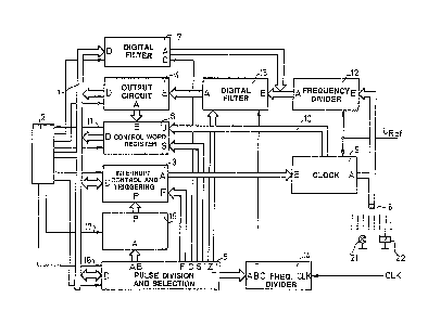
A-509 1 31~ ~ 9 9
Fig. 1 shows a block diagram of a system for input
and/or output;
Fig. 2 shows an output circuit;
Fig. 3 shows a pulse frequency divider;
Fig. 4 shows two specimen embodiments of an output
stage and of an adapter circuit;
Fig. 5 shows a further specimen embodiment of an
adapter circuit;
Fig. 6 shows a digital filter;
Fig. 7 shows an input circuit with interrupt if the
input signal changes;
Fig. 8 shows an interrupt-triggering circuit; and
Fig. 9 shows a third specimen embodiment of an
adapter circuit.
The circuits shown in Fig. 2 to 9 form the most
important components of the system as detailed in
Fig. 1. The circuits are in each case designed for
eight parallel signals. With few exc~ptions, Fig. 2
to 9 show merely switching operations for one of the
eight parallel signals. Identical components in the
figures are provided with identical reference numbers.
Fig. 1 shows the block diagram of an input/output
system according to the invention which is part of a
A-509 - ]0 -
~314~99
digital control system. The digital control syste~
may comprise more than one of the input/output systems
shown in Fig. 1, one or more microprocessors as well
as memories and other components. To describe the
invention, of the other components of the digital
control system, only a data bus 1 and a control unit 2
are shown.
Connected to the data bus 1 are an output circuit 3,
an input circuit 4, a control-word register 5, a
circuit 6 for triggering an interrupt of the program
run and a test-pattern register 7. These units are
also connected to the control unit 2 via control
lines, of which only one is indicated in each case in
Fig. 1. It is also possible to provide an address and
control bus for the thus transmitted signals. In the
specimen embodiment, the units 3 to 7 and the data ¦~
bus 1 are each designed for a width of 8 bits. ,
, i
Supplied via the data bus 1 to an output circuit 3 are i!
signals which are finally to be sent to loads 21, 22
via an input/output 8. Individual bits of the
eight-bit-wide input/output 8 can be set by program as
an input or output. In larger systems, however, it
will be preferable to operate one or more of the
circuits shown in Fig. 1 as output circuits and others
as input circuits.
With regard to the control of machines and plants, the
loads 21, 22 that are to be connected to the
inputs/outputs will primarily be indicator lamps and
magnetically operated actuators. With such machines
and plants, it has proved advantageous to show ~¦
particularly important signals by the flashing of
- lt - 131~99
indieator la~ps. The flashing of several indicator
lamps, ~hich are eontrolled by a mieroprocessor,
results, however, in a very eonfusing pieture, since
the timing of the flashing of all indieator lamps
varies depending on the program.
For this reason, in a further development of the
invention, provided in the output circuit 3 is a
linking of the signals with flashing signals that can
be generated separately for each bit of the data word
supplied to the output circuit 3. For this purpose, a
control word is supplied via the data bus 1 to a
control-word register 5, said control word indicating,
among other things, which bits o~ the data word to be
sent via the output circuit 3 are to flash. In this
connection, it is also possible for various bits to
flash at different frequencies. Further details in
this regard will be explained later in conjunction
with Fig. 2 and 3.
The output signals of the output circuit 3 are sent to
an eight-bit output-stage circuit 9, further detalls of
which are described in conjunction with Fig. 4.
The output-stage circuit 9 is short-circuit-proof and
is provided with a circuit for measuring the output
eurrent. The outputs of the output-stage circuit 9
form the input/output 8. If a predetermined output
current is exceeded, a circuit 6 for triggering an
interrupt of the program (interrupt triggering) is
activated via detector 90 associated with resistor 89
and any signal outputted to data line 10. The circuit
6 is conneeted via a line 11 directly to the eontrol
unit 2 of the digital eontrol system, where the program
currently being executed is interrupted in order to
change over to an error-diagnosis program.
A-509 -- 12 - 1314 5 9 9
From the input/output 8, Olltput signals and/or input
signals from sensors, for example limit switches or
emergency-stop switches, said signals having to be
monitored, are sent to an adapter circuit 12. The
primary task of this circuit is to adapt the levels of
the input signals, which may have been sent over long
lines, to the level of the digital system, for example
TTL. In this connection, it is possible, to a certain
extent, for noise interference superimposed by
threshold-value characteristics to be suppressed and,
through the use of differential amplifiers, for
signals that have been transmitted symmetrically on
two lines from the sensor to the adapter circuit 12 to
be further-transmitted on one line.
;
Furthermore, an embodiment of the adapter circuit 12
has a special feature which consists in that a ;
reference potential is supplied to it. Connected to
this reference potential are the terminals of the
sensors facing away from the inputs/outputs 8.
Depending on whether this reference potential
corresponds to the operating voltage of, for example, !,
+24 V or to the frame potential, such an adaptation ~
takes place in the adapter circuit 12 that, at the ¦
outputs of the adapter circuit 12, the same logic
level is always assigned to a predetermined circuit
state of the sensor.
The output signals from the adapter circuit 12 are
supplied to a digital filter 13, which suppresses
signals that are so short that they cannot be
"genuine" signals from a sensor. To adapt the digital
filter 13 to the respective sensor, both the frequency
of the clock signal and also the number of clock
,1
A-509 - 13 -
1314~99
pulses for filtering are controlled. Once again,
control is effected via the control-word register 5,
which, firstly, provides the number of clock pulses
and, secondly, supplies a di~ider value to a frequency
divider 1~.
The signals that have passed the digital filter 13 are
supplied via the input circuit 4 to the bus system 1
and to the interrupt-triggering ciruit 6. To monitor
the digital filter 13 and the input circuit 4, signals
representing a test pattern are supplied from the bus
system 1 via a test-pattern register 7 to the input of
the digital filter 13.
If the system is used for output, the signals that are
to be sent on to the loads ~1, 22 are each sent as one
bit of an eight-bit word via the bus system 1, the
output circuit 3 and the output-stage circuit 9 to the
output. Some of them are pulsed, for which purpose .
the necessary pulses are supplied to the output
circuit 3 via the control-word register 5 and a pulse
frequency divider 15. If a load is off, 24 V is
applied to the corresponding terminal of the
input/output 8, while, with the load on, 0 V is
applied. This information is supplied via the adapter
circuit 12 and the digital filter 13 to the input
circuit 4, from where it can be interrogated, when
desired, by the control unit via the bus system 1, so
that it is possible to monitor regularly whether the
desired ~olta~es are present at the input/output 8.
~-509 - 14 -
~31~99
Errors which, for e~ample, are caused by the output
circuit 3, the output-stage circuit 9 or by the load
in question, are detected. To ensure that a
corresponding error indication or other suitable
measures are not effected only when the input circuit
4 is interrogated within the course of the normal
operation of the program, the input circuit 4 is
connected to the interrupt-triggering circuit 6. In
addition, there is a direct report from the
output-stage circuit 9 if a short circuit, i.e. an
excessively high output current, is taken from one of
the output stages.
In addition, the digital filter 13 and the input
circuit 4 are checked regularly - for example whenever
the control system is started up - by the connection l
of a test pattern to the inputs of the digital filter ¦
13. Thus, i~ the input~output system is operated as
an output, it is possible to differentiate whether, in j I
the case of an error occurring in the loop formed by ,
the output circuit 3, the output-stage circuit 9, the 1l ~;
adapter circuit 12, the digital filter 13 and the
input circuit 4, it is the path for the output signals
and/or the path for the input signals that is
defective.
To operate the system shown in Fig. 1 as an input,
sensors, preferably switches, are connected to the
terminals of the input/output 8. No output signals
are supplied via the output circuit 3, and the input
signals from the sensors are, as already described in
conjunction with the checking of the output signals,
supplied via the adapater circuit 12, the digital
filter 13 and the input circuit 4 to the bus system 1.
A--509 -- 15 - ~3~
In the following, the operating principle of the
system shown in Fig. 1 is explained with reference to
the details presented in Fig. 2 to 8. The output of
signals, the further transmission of input signals,
the checking of the system as well as the triggering
of an interrupt are described in the following
individual sections.
Output of signals
From the control unit 2, eight signals are sent in
parallel via the data bus 1 to the output circuit 3
for the driving of eight loads. Only two of the eight
loads are shown, namely a bulb 21 and a relay winding
22. Shown in Fig. 2 is merely one of eight parallel
channels of the output circuit 3. The data inputs D
of two registers 31, 32 are connected to the data bus
1 via the connection 33 ~Fig. 1). Via further inputs
34, 35, signals CSl and CS2 are supplied from the
control unit; these signals can be used, for one data
word in each case, to energize the registers 31 or the
registers 32 to accept the input signals D. An
enabling signal Fl is supplied, likewise from the
control unit 2, via a further input 37. Furthermore,
for each of the parallel channels, an input 38 is
provided for a pulse signal which, together with the
output signal of the register 32, is supplied to the
NOT-AND circuit 39, which, in turn, together with the
output of the register 31, is connected to an AND
circuit 40. From the output 41, the respective signal
is supplied to the output-stage circuit 9 (Fig. 1).
A--~09 - 16 - 131~ 5 9 ~
The seek signals CSl and CS2 are supplied to the
G-inputs of the registers 31 and 32 via AND circuits
42, 43, to which a write pulse WR is additionally
supplied via an input 44 if data are to be written
into the egisters 31 or 32. The data stored in the
registers 31 and 32 can, however, also be read via the
data bus 1 (Fig. 1). For this purpose, tristate
drivers 45, 46 are connected to the outputs ~ of the
registers 31, 32; the outputs of these tristate
drivers 45, 46 are connected via the respective
connection 33 to the data bus. If the contents of one
of the registers 31 or 32 is to be read, a read pulse
RD is supplied via an input 47 to the two ~ND circuits
48, 49, whereupon the corresponding seek pulse CSl or
CS2 is sent to the output-control connection OC of the 1¦
tristate driver 45 or 46.
This reading-out of the contents of the registers 31
and 32 is particularly advantageous if the control
unit has several computers. It may happen in this
connection that one computer is responsible for
driving an output circuit, with some of the parallel
output signals being accepted and others being changed
according to the program of the receiving computer.
The receiving co~nputer is then able to read the
register contents in order then via the data bus 1 to
send a new data word in which the corresponding bits
are unchanged.
~-5Q9 - 17 -
l3l~99
If the output 41 is to be off, a logic 0 is stored in
the register 31. The state of the register 32 is then
without significance. If the output 41 is to be
permanently on, a logic 1 is stored in the register 31
and a logic 0 in the register 32. This logic 0
results at the output of the NOT-AND circuit always in
a logic 1, which, together with the output of the
register 31, constantly switches on the output 41 Yia
the AND circuit 40. If an output signal is to be
pulsed, in order, for example, to make a warning lamp
flash, the pulse signal P1 supplied via the input 38
is sent via the N~T-AND circuit 39 through the
register 32 (set to logic 1~ to the AND circuit 40.
Together with the register 31 (set to logic 1), there
results via the AND circuit 40 at the output 41 a
pulsed driving si~nal ~or the output circuit 9.
Fig. 3 shows a block diagram of the pulse frequency
divider 15, to which a pulse clock signal is supplied
at 51. The frequency of this pulse clock signal
corresponds t~ the highest required pulsing/flashing
frequency of an indicator lamp. Flip-flops 52, 53, 54
form a frequency-divider chain. ~oth the input 51 and
the outputs of the flip-flops 52, 53, 54 are connected
to inputs of eight multiplexers, of which only one
multiplexer 55 is shown in Fig. 3.
Via further inputs 56, 57, a two-bit-wide control word
is supplied to the multiplexer 55 from the
control-word register 5 (Fig. 1). Further similar
2-bit ~ontrol-word inputs are connected to the
multiplexers not shown. Depending on the control
word, the output 58 of the multiplexer 55 is connected
to one of the multiplexer inputs, so that the pulsing
or flashing frequency can be varied in each case by a
factor of 2.
,~
i
A-509 - 18 - 131~5~9
Fig. 4a and b show two embodiments of output stages,
of which eight are provided in each case in the
o~ltput-stage circuit 9 (Fig. 1). Provided in the
output stage shown in Fig. 4a is a transistor 61,
which, apart from the load 62, does not have any load
resistance. The output 63, therefore, represents a
so-called open-collector output. From the output
circuit 3 ~Fig. 1) the signal is sent to the input 64
of the output stage shown in Fig. 4a and is supplied
via a driver 65 (shown only diagrammatically) to the
base of the transistor 61. Connected in series with
the collector-emitter circuit of the transistor 61 is
a current-measuring resistor 66, which is bypassed by
the base-emitter circuit of a further transistor 67.
In the case of a short circuit in the load 62, the
voltage drop across the resistor 66 becomes so great
that the further transistor 67 starts to conduct aDd
there is a voltage drop across the resistor 68, said
voltage being transmitted via a threshold-value switch
69 and one o~ the leads 10 (Fig. 1~ to the
interrupt-triggering circuit 6. Via this circuit, it
is possible ~or the output circuit to be driven in
such a way that the output stage becomes de-energized.
For various reasons, for example because of le~gthy
lines between the overall electronic control system
and the individual loads, an operating voltage o
+ 24 V is usually provided for the loads. It is
possible, however, also to use other voltages. To
check the output circuit, therefore, an adaptation to
the digital circuits used, for example TTh circuits,
is necessary. This purpose is served by the adapter
circuit 12 (Fig. 1), of which Fig. 4a shows the
circuit 70 for one of eight bits.
A-509 - 19 - ~3i~599
Adaptation is performed basically by a voltage divider
71, 72, to which a comparator 73 or a threshold-value
switch is connected. The output 74 of the comparator
is connected to a digital filter 13 (Fig. 1), which is
described in greater detail later in conjunction with
Fig. 6. From the digital filter the signals are
supplied to the input circuit 4 (Fig. 1) and can be
read by the control unit 2 via the data bus 1.
In the system according to the invention, it is
possible to detect the following defects on the path
of the siynals (for driving the loads~ between the
control unit 2 and the respective load 62:
1. An open circuit between the control unit and the
transistor 61 in the output stage does not, in
spite of different signals supplied from the
control unit, cause any change in the signals read
out from the input circuit 4 (Fig. 1~.
2. In the case of an open circuit in the lead between
the output 63 and the load 62 or in the further
lead to the operating-voltage source, frame
potential is always connected to the output 6~.
Explained in conjunction with Fig. 4b is a further
embodiment of the invention which makes it possible
for loads with the same output stage to be connected
by their terminals facing away from the output either
to a positive operating voltage or to frame
potential. This may be advantageous particularly if a
digital control system with the input/output system
according to t.he invention is connected to printing
presses in which loads, including the wiring, are
already present. Also if several printing presses or
printing-press components are controlled by a digital
control system, it is possible for loads and sensors
to be connected to different potentials.
A-509 - 20 - 131~9~
With the output stage according to Fig. 4b, two
series--connected transistors 82, 81 form the output
stage together with a driver circuit 83 (shown only
diagrammatically). The transistors can be driven in
such a way that the output 84 forms a so-called
tristate output. In this connection, the output 84 is
of high resistance, i.e. both transistors 81, 82 are
non-conducting when no voltage is suppl;ed to a load
85, which, in the case of Fig. 4b, is shown as a relay I
winding. The connection ~6 of the load 85 facing away
from the output 84 is connected to a control input 87
of the driver circuit a3. This means that, when a
positive voltage is present at the connection 86, the
transistor 81 is controlled by the signals applied to
the input 88 of the output stage. If, however as
indicated by the broken line in Fig. 4b, the
connection 86 is connected to frame potential, the !
driver circuit 83 is switched over to the transistor
82, with the result that the latter is controlled by
the signals supplied at 88. With the adapter circuit
92 shown diagrammatically in Fig. 4b, account is
likewise taken of whether the load 85 is connected to
positive potential or to frame potential, for which
purpose the reference potential is supplied to a
control input 91 of the adapter circuit 92.
Further transmissiQn_ Qf input siqnals
The following explanatory remar~s refer to the further
transmission of input signals via the adapter circuit
1~, the digital filter 13 and the input circuit 4. In
this connection, the input signals may originate from
sensors, for example switches, which are disposed on
the machine being controlled. However, they may also
be output signals from the output stage 9 that are to
1'
A-5~9 - 21 -
131~9~
be checked. While Fig. 4a shows a first embodiment of
an adapter circuit in conjunction with an output
stage, Fig. 5 shows a second embodiment of an adapter
circuit, to which input signals are supplied from a
sensor 96 via two leads to a differential input. The
latter may be advantageous particularly in the case of
sensors that perform safety-relevant and rapid
functions.
The sensor 96 is a so-called pole-changing switch and
is connected with its wipers to frame potential and
+ 24 V, so that the wires leading to the inputs 97 and
98 can be connected alternately to frame potential and
+ 24 V. The inputs 97, 98 are connected, each via a
voltage divider 99, 100; 101, 102 to a non-inverting
and an inverting input of a differential amplifier
103, the output 104 of which forms an output of the
adapter circuit.
From the adapter circuit 12 eight parallel input
signals are sent to the digital filter 13. Fig. 6
shows an embodiment of one of eight filters provided
in the circuit 13. The filter serves to suppress
interference through contact bounce and through noise
pulses on the lines. It transmits an input signal
further only if its value does not change during the
filtering time.
The signal to be filtered is supplied to the input
161, while the clock signal T is supplied at 162.
Supplied to the inputs 163, 164 and 165 from the
control-word register 5 (Fig. 1) are signals that
chara`cterize the number of clock pulses on which
filtering is based. These signals pass via inverters
A-509 - ~2 - ~ 9
166, 167, 168 to the inputs A, B, C of the counter
169. The input and output designations refer to a
counter of type 161.
The clock signal supplied at 162 pulses a first
flip-flop 170 and the counter 169 and is supplied via
an inverter 171 to the clock input of a second
flip-flop 172. Four NOT-AND circuits 173, 174, 175
and 176 form a multiple~er, which, depending on the
instantaneous level of output Q of the flip-flop 172,
transmits either the output signal Q of the flip-flop
170 or the output signal QD of the counter 169 to the
input D of the counter 169. The output of the
multiplexer as well as the output Q of the flip-flop 1,
170 are connected to the inputs of an exclusive-OR~ ¦
circuit 177, the output of which is connected to the I 1
LOAD input of the counter 169. ~ ¦~
With an unchanged signal at the input 161, the signal
at the output of the NOT-AND circuit 176 is returned
via the multiplexer to the D-input of the counter.
Since the input and output signals are equal, LOAD is
low. If the signal at the input 161 changes, the
signal at the LOAD input becomes high and the counter
169 starts to count. With a predetermined filter
number of 3, the counter status is 4.
If the input signal returns to its old state before
the counter 169 reaches the value 7, LOAD becomes low
again and filtering is discontinued.
When the counter reaches its final count 7, the high
level is applied via the tripple AND circuit 179 to
A-509 - 23 -
131~99
the D-input of the flip-flop 172. At the next
negative edge of the clock signal, output Q of the
flip-flop 172 assumes the high level and switches the
multiplexer to the Q-output of the flip-flop 170, so
that the then current level of the input signal is
applied to the D-input of the counter 169. LOAD
becomes low again, since there is equality between
input and D-input of the counter 169, and connects the
input information through to the output 178. At the
same time, the D-input of the flip-flop 172 becomes
low through the loaded filter number 3. At the next
negative eage of the clock signal, the output Q of the
flip-flop ].72 likewise becomes low and switches the
multiplexer, so that once again the output signal of
the counter 169 is returned to its D-input.
1,
Ei~ht parallel output signals of the digital filter 13
(Fig. 1) are supplied to the input circuit 4. A
specimen embodiment of the input circuit is explained
in the following with reference to Fig. 7, which shows
one of the eight channels in the input circuit 4. The
output signal of the digital filter 13 (Fig. 1) is
supplied at 121 and can be supplied via a tristate
driver 122 and the output 123 to the data bus 1 (Fig.
1). For this purpose, a seek signal CS is supplied
via a control input 124 to the tristate driver 122.
Via an input 127, the system clock CLK is sent to the
clock inputs of two flip-flops 125 and 126. With the
flip-flops 125, 126, the input signal is delayed in
each case by one clock period. With the aid of a
non-equivalence circuit 129 it is determined whether
the input signal has changed from one clock to the
next. If this is the case~ a signal to trigger an
interrupt is sent from the output 130.
A-50~ - 24 -
131~9
Che~kinq the system
As already explained in con]unction with the output of
signals and peripheral units, the reading-in of the
signals that have been output provides a first
possibility ~or checking the input/output system. A
further check is performed in that test patterns can
be applied to the inputs of the digital filter and in
that the thus generated output signals of the input
circuit 4 are checked for agreement. This increases
safety and reliability when the system according to
the invention is used for input. In addition, this
allows more accurate pin-pointing of errors when the
system according to the invention is used ~or output.
For the connection of the test pattern, the cGntrol
unit 2 (Fig. 1) writes a test pattern into the
test-pattern register 7 via the data bus 1, and the t
test pattern 7 is supplied to the inputs of the
digital filter 13. The time at which the test pattern I
is connected is determined by a control bit in the ¦
control-word register S. The test-pattern register 7
can be implemented in simple manner with obtainable
components, so that a further egplanation is
unnecessary. It contains basically an eight-bit
register with tristate outputs.
It is practical for the test pattern to consist in
that a value 1 occurs consecutively in the eight
parallel channels, with the other channels being set
to zero. Thus, among other things, each of the
channels being checked is tested for a connection with
the neighbouring channel.
' ~1
A-50~ - 25 -
1314~99
Interrupt triggering
The input circuit 4 and the output-state circuit 9
each send eight parallel signals to the circuit 6 for
interrupt triggering. One signal from the input
circuit 4 passes via an input 141 (Fig. 8) to the
J-input of a JK flip-flop 143, into which the signal
is loaded with a clock CLK supplied at 145. One of
the signals supplied from the output-stage circuit 9
(Fig. 1) is sent via an input 142 to a JK flip-flop
144, into which it is likewise loaded with the clock
CLK. If a 1 is present at one of the outputs of the
16 flip-flops 143, 144, an interrupt signal is sent to
the control unit via the 16-~it O~ circuit and the
output 147.
In systems with several circuits for triggering an
interrupt, the control unit interrogates the
individual circuits in turn to find out which input
has triggered the interrupt. This is known as
polling, in which, with the circuit shown in Fig. 8,
the outputs of the flip-flops 143, 144 are
interrogated consecutivel~ via the registers 150, 151
by the seek pulses CSl and CS2 supplied at 153 and
156. The outputs of the registers 150, 151 are each
connected to a lead of the data bus via the connection
152. During the reading-out of the registers 150,
151, their D-inputs are disabled, so that the
resetting of the flip-flops 143, 144 does not change
the contents of the registers 150, 151.
Via the inputs 154, 155 and the OR circuits 148, 149,
signals Sl and S2 can be supplied from the
control-word register 5 (Fig. 1) to the reset inputs
of the flip-flops 143, 144, these signals making it
possible to suppress the further-transmission of
individual error signals.
A-509 - 26 -
131~99
Within the framework of the invention, the triggering
of an interrupt may also be performed via an interrupt
controller, which supplies an interrupt vector to the
control unit.
With the aid of the adapter circuit shown in Fig. 9,
the signal of a sensor, for example of a switch 181,
can be received irrespective of whether the connection
of the switch 181 facing away from the input 182 is
connected to frame potential or to a reference voltage
differing from frame potential. A system according to
the invention provided with such an adapter circuit
can be used for controlling a machine in which there
is even a mix of both types of connection, for
example, when machine complexes of different product
lines are connected together, without this requiring
separate adaptation of the circuits or of the program
to the sensors.
For automatic adaptation to the various modes of
operation of the sensors, the reference voltage
(either frame potential or a voltage differing from
frame potential) is supplied via an input 183 and a
voltage divider 184, 185 to the control input of a
contxollable two-pole selector switch 186. If the
reference voltage differs from frame potential, the
selector switch is in the upper position identified by
the solid line.
In addition, the output voltage of the voltage divider
184, 185 is supplied to inputs of two threshold-value
switches 189 and 193 - in negated form to the
A--509 - 27 -
1314~99
threshold-value switch 193. This means that the
output signal of the threshold-value switch 189 is
transmitted further to the output 190 if there is a
positive voltage at the voltage divider 184, 185. The
output of the threshold-value switch 193 is disabled
in this case. Preferably, use is made in this
connection of a threshold-value switch with a
so-called tristate output, which has high resistance
when there is a corresponding signal at the input. If
the voltage at the voltage divider 184, 185
corresponds to frame potential, the output voltage of
the threshold-value switch 193 is transmitted further
to the output 190, while the output of the
threshold-value switch 189 is disabled. The
threshold-value switches 189, 193 differ in that the
threshold-value switch 189 does not make any inversion
between the input and output signals, whereas an
inversion is provided with the threshold-value switch ;
When the switch 181 connected to + 24 V is activated, !
the positive voltage is supplied via the voltage
divider (formed by the resistors 187, 188) to the
inputs of the threshold-value switches. Thereupon,
the threshold-value switch 189 likewise sends positive
potential of, for e~ample, 5 V to the output 190.
With the switch 181 open, there is 0 V at the input of
the threshold-value switch 189, so that the output
voltage is also 0 V.
If, however, instead of the switch 181~ a switch 191
connected to frame potential is connected to the
adapter circuit and, at the same time, the point 183
is likewise connected to frame potential, the selector
switch 186 is in the lower position and the
1,
A-509 - 28 -
~31~99
threshold-value switch 193 is active. In this case,
with the switch 191 open, the voltage of ~ 5 V
supplied via the input 192 and the resistor 188 is
present at the input of the threshold-value switch
193. The output voltage of the threshold-value switch
193 and thus the voltage at the output 190 is then
0 V. If the switch 191 is closed, frame potential is
applied to the input of the threshold-value switch
193, with the result that the output voltage is then
5 V.
Irrespective of whether the switch in question is
connected to frame potential or to a positive
operating voltage, therefore, the adapter circuit
shown in Fig. 9 supplies one logic level when the
switch is closed and the other when the switch is
open. Together with a control system, therefore, both
types o~ sensors (switch to frame, switch to positive~
can be used alternatively or in combination, without
this requiring a special adaptation o~ the circuits or
of the program to the sensors. Interrogation by
program as to whether the sensors are connected to
frame or to positive is also unnecessary.
``1 ~3~4~99
1 = Test-pattern connection
2 = I nput circuit
3 = Interrupt control and triggering
4 = Output circuit with pulse connection and enabling
5 = Pulse division and selection
6 = Control-word register
7 = Digital filtering
8 = No. of clocks
9 = Clock
10 = Input-voltage adaptation
11 = Short-circuit-proof output stages with current
measurement
12 = Frequency divider
13 = 16-bit OR