Note: Descriptions are shown in the official language in which they were submitted.
~L31~97~
TIME AXIS CORRECTING DEVICE
The present invention generally relates to a time axis
correcting device for use in a video tape player, or the like,
for minimizing or substantially eliminating change in time
axis that is caused in a video signal as a result o~ a change
in speed.
To enable the prior art to be described with the aid of
diagrams the figures of the drawings will first be listed.
Fig. 1 is a block circuit diagram of a time axis
correcting device according to a preferred embodiment of the
present invention;
Fig. 2 illustrates a waveform representing sampling
values of a sine wave adapted to be written in a read-only
memory;
Fig. 3 is a block circuit diagram of the prior art time
axis correcting device;
Fig. 4. illustrates a waveform of a signal used to
explain the manner by which the phase of a sampling clock
signal is calculated; and
Fig. 5 is a block circuit diagram showing the prior art
clock phase modulating means.
Fig. 3 illustrates a prior art time axis correcting
device in a block circuit representation.` This prior art time
axis correcting device is disclosed in "VTR Gijutsu (VTR
Technology)~ r page 118, Edited by Nippon Hoso Shuppan Kyokai
and comprises an analog-to-digital (A/D~ converter 1, a memory
unit 2, a digital-to-analog (D/A) converter 3, a write-in
clock generator 4 and a read-out clock generator 5.
This prior art time axis correcting device operates in
the following manner. Assuming that a video signal having its
time axis varying is inputted to the write-in clock generator
4, the write-in clock generator 4 outputs a write-in clock
signal conforming to the change in time axis. The write-in
signal emerging from the write-in clock generator 4 is in turn
9 7 ~
applied to the analog-to-digital converter 1 which functions
to sample the input video signal and converts the input video
signal into a PCM signal, the sampled value being subse~uently
stored in the memory unit 2. On the other hand, in the read-
out clock generator 5, a clock signal necessary to read out
data from the memory unit 2 in synchronism with a reference
synchronizing signal applied thereto from an external terminal
12 is synthesized. Therefore, in synchronism with the read-
out clock signal generated from the read-out clock generator
5, the data stored in the memory unit 2 can be read out
therefrom and is in turn supplied to the digital-to-analog
converter 3 for the conversion of the data into an analog
signal.
By the process described above, the change in time axis
can be substantially removed from the input video signal and
an output video signal having its time axis stabilized in
synchronism with the external reference signal can be
obtained.
The write-in clock generator referred to above is
available in numerous models. For example, Japanese Laid-open
Patent Publication No. 58-124386, published in 1983, discloses
a write-in clock generator of a type wherein means is provided
for detecting, and responding at a high speed to, change in
time axis in dependence on a burst si~nal contained in the
input video signal.
Fig. 4 illustrates a waveform used to explain the
principle of detection of a deviation of sampling points
resulting from the change in time axis. Referring to Fig. 4,
if the cycle of a sine wave represented by khe burst signal is
four times the sampling cycle, the sampling of the burst
signal will give four sampling points per cycle as shown.
Assuming that the sampling points shown in Fig. 4 have
respective levels expressed by Xl, X2, X3 and X4, the
following relationships can be established:
Xl = B + A-sin~
X2 = B + A-sin(~ + 90) = B + A cos~
X3 = B -~ A sin(~ + 183) = B - A-sin~
,~
~314~7~
X4 = B + A-sin(~ + 270) = B - A cos~
wherein A represents the amplitude of the burst signal, B
represents the direct current level of the burst signal and
represents the phase of the sampling point corresponding to
the level X1 o~ the sampling point.
Accordingly,
X1 - X3 = 2A sin~, and
X2 - X4 = 2A cos~
and, therefore, the phase ~ of the sampling point can be
determined from the four sampling points as expressed by the
following equation:
~ = tan-1(X1 - X3)/(X2 ~ X4).
If ~ = 0 is taken as the reference to the sampling point, the
calculation of the phase 9 of the sampling point can provide
an indication of the deviation (phase difference) of the
sampling point from the reference point. In view of this, by
varying the phase of the sampling clock signal (sampling
command signal) according to the calculated phase G (phase
difference) of the sampling point, the write-in clock can be
obtained which corresponds to change in time axis.
The above mentioned patent publication also discloses a
phase modulating means as a means for varying the phase of the
sampling clock signal. This phase moclulating means is
reproduced in Fig. 5 in a block circui.t representation.
Referring now to Fig. 5, the phase modulating means includes
delay elements 34, 35, 36, 37, 38, ancl 39, each of the delay
elements 34 to 36 having a delay amount equal to 1/4 of the
cycle of the sampling clock signal while each of the delay
elements 37 to 39 has a delay amount equal to 1/16 of the
cycle of the sampling clock signal. The phase modulating
means disclosed therein also includes data selectors 31 and 32
and a buffer amplifier 33.
In the above described phase modulating means, the delay
elements 34 to 36 weighted to have a delay amount equal to 1/4
of the cycle of the sampling clock signal are connected in
series with each other with input and output terminals o~ each
delay elements 34 to 36 connected to input terminals of the
data selector 31, and similarly, the delay elements 37 to 39
weighted to have a delay amount e~ual to 1/16 of the cycle of
the sampling clock signal are connacted in series with each
other with input and output terminals of each of the delay
elements 37 to 39 connected to input terminals of the data
selector 32. A reference clock signal is applied to an input
of the phase modulating means through the buffer amplifier 33.
This phase modulating means is so designed that a data
corresponding to the amount of delay of the clock signal
determined in reference to the phase e of the sampling point
so calculated by the above described method is applied, as a
fine time axis error signal, to the data selectors 31 and 32
there~y to modulate the phase of the sampling clock signal.
In the prior art time axis correcting device of the
construction described hereinabove, the circuit shown in and
described with reference to Fig. 5 has been employed as a
sampling clock modulating means capable of responding at high
speed to the change in time axis contained in the input video
signal. The use of the sampling clock modulating means of the
type discussed above has a problem in that the amounts of
delay exhibited by the data selectors 31 and 32 must be
exactly matched with the delay characteristics of the delay
elaments 34 to 39, requiring time-consuming and cumbersome
adjustment.
~ccordingly, the present invention has been devised with
a view to substantially eliminating the above discussed
problems inherent in the prior art time axis correcting device
and has for its primary object to provide an improved time
axis correcting device of a type wherein the cloc~ phase
modulating means used to vary the phase of the sampling clocX
signal does not require any adjustment of the phase modulation
and is rendered highly precise.
The time axis correcting device herein provided in
accordance with the present invention is operable to
substantially remove the change in time axis in the input
video signal and, for this purpose, comprises a video signal
storage means; a write-in control means operable in response
13~97~
to a sampling command signal to write the input video signal
in the video signal storage means at a write-in timing
conforming to the change in time axis in the input video
signal; a read-out control means for reading out the video
signal from the video signal storage means at a predetermined
read-out timing; a waveform storage means for storing sampling
data obtained by sampling a sine wave at predetermined
intervals; a reference signal sampling means for sampling the
reference signal from the input video signal; an address
control means for calculating the difference in phase between
a sampling point and a reference position for the sampling
point according to a sampling value of the reference signal
sampled from the input video signal and also for addressing
the waveform storage means according to the difference in
phase to cause the waveform s~orage means to output the
sampling data of the sine wave; and a signal converting means
for converting the sampling data of the sine wave into the
sampling command signal.
Preferably, the time axis correcting device according to
the present invention may include a sync separator circuit
operable to separate a horizontal synchronizing signal from
the input video signal so that the horizontal synchronizing
signal can be applied to the reference signal sampling means
to allow the latter to sample the reference signal at
predetermined intervals from the horizontal synchronizing
signal.
Preferably, the horizontal synchronizing signal may be
used as a reset signal for resetting the write-in control
means, and the reference signal may be a color burst signal.
Pre~erably, the address control means may comprise a
calculating circuit for calculating the difference in phase
and for providing a phase difference signal indicative of the
difference in phase, an address generator for generating a
reference address signal, and an adder for summing the phase
difference signal from the calculating circuit and the
reference address signal together to provide an address signal
to be applied to the waveform storage means. The waveform
13~4~
storage means may preferably comprise a read-only memory.
According to the present invention, the amount of
modulation in phase of the sampling clock signal can be
calculated from the sampling value of the reference signal in
the input video signal, and the sampling data of the sine wave
can be read out from a read-only memory according to the
calculated value. The sampling data of the sine wave is
subsequently converted to provide the sampling command siynal
having its phase modulated. The sampling command signal so
obtained is highly precisely modulated in phase with no
adjustment substantially effected thereto, and therefore, a
highly stabilized operation can be appreciated.
In any event, the present invention will become more
clearly understood from the following description of a
preferred embodiment thereof, when taken in conjunction with
the accompanying drawings. However, the embodiment and the
drawings are given only for the purpose of illustration and
explanation, and are not to be taken as limiting the scope of
the present invention in any way whatsoever, which scope is to
be determined solely by the appended claims.
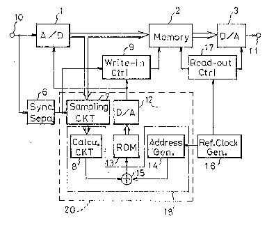
Referring now to Fig. 1, the analog-to-digital (A/D)
converter 1 shown therein is adapted to convert into digital
data the video signal with varying time axis inputted thereto
through an input terminal 10. The digital data converted by
and outputted from the analog-to-digital converter 1 is
subsequently stored in the digital memory unit 2. The
digital-to-analog (D/A) converter 3 connected to the digital
memory unit 2 is used to output, from an output terminal 11, a
video signal having its time axis corrected, that is, a video
signal from which variation in time axis has been
substantially remo~ed. A synchronizing signal contained in
the input video signal, that is, the video signal appli~d to
the input terminal 10, is separated from the input video
signal by a sync separating circuit 6.
The synchronizing signal separated by the sync separating
circuit 6 from the input video signal as hereinabove described
is supplied to a clock phase modulating means. This clock
'` ;'`~`
~1497'~
phase modulating means is comprised of a burst sampling
circuit 7 for extracting, and applying to a calculating
circuit 8, a predetermined reference signal which is, for the
purpose of time axis correction, inserted in the input video
signal emerging from the analog-to-digital converter 1, that
is, a data representative of a burst signal component. It is
to be noted that, so far as the input video signal is based on
the NTSC scheme, the burst signal component may be a color
burst signal. The calculating circuit 8 connected with the
burst sampling circuit 7 is operable to calculate the
difference in phase.
A write-in control circuit 9 is operable to control a
write-in operation of the digital memory unit 2 and is
connected with a digital-to-analog (D/A) converter 12 which
outputs to the write-in control circuit 9 a clock signal (a
sampling command signal) having its phase modulated by the
phase difference calculated by the calculating circuit 8.
Connected to the digital-to-analog converter 12 is a read-only
memory (ROM) 13 in which sampling values of a sine wave are
stored. Reference numeral 14 represents an address generator
for generating a reference address signal to be applied to the
read-only memory 13 through an ad~er 15 which is also adapted
to receive the output from the calculating circuit 8.
Connected to the address generat,or 14 is a reference clock
generator 16 connected not only with the address generator 14,
but also with a read-out control circuit 17 operable to
control the reading of the data out from the digital memory
unit 2.
It is to be noted that a block shown by the single dotted
line 18 in Fig. 1 represents an address control means for the
read-only memory 13 whereas a block represented by the broken
line 20 represents the clock phase modulating means.
~ hile the time axis correcting device according to the
present invention is so constructed as hereinabove described,
it operates in the following manner.
The input video signal having its time axis varying is
applied through the input terminal 10 to both of the analog-
,~'
~3~7~
to-digital converter 1 and the sync separating circuit 6.
Upon receipt of the input video signal, the sync separating
circuit 6 separates a horizontal synchronizing signal from the
input video signal. The horizontal synchronizing signal so
separated is in turn applied to both of the memory write-in
control circuit 9 and the burst sampling circuit 7. The
memory write-in control circuit 9 then generates a write-in
address for the memory unit 2 so that the address can be reset
in synchronism with the horizontal synchronizing signal to
perform a time axis correction for each horizontal scanning
period. On the other hand, the burst sampling circuit 7
extracts sampling values of the burst signal at a
predetermined interval subsequent to the receipt of the
horizontal synchroni~ing signal, which values are subsequently
supplied to the calculating circuit 8.
In the calculating circuit 8, the difference in phase
between the sampling points and the reference position of the
sampling point is calculated according to the previously
described method. After this calculation, the calculating
circuit 8 outputs a phase difference signal. The phase
difference signal is then supplied to the adder 15 at which
the phase difference signal is summed together with the
reference address signal generated from the address generator
14 on the basis of the reference clock signal.
The read-only memory 13 has been programmed to store data
obtained by sampling a sine wave at a predetermined interval,
for example at equal interval. By way of example, the
sampling points in the case where 16 sampling points are
sampled during one cycle of the sine wave, respective values
of which are sequentially written in the read-only memory 13,
are such as shown in Fig. 2, and numerals affixed to the
respective sampling points shown in Fig. 2 correspond to
addresses.
In the example shown in Fig. 2, addresses of the read-
only memory are designated 0 to 15, and arrangement has been
made that the address generator 1~ can generate a numerical
value varying in four stages at four address intervals, that
.~
~31~7~
is, 0, 4, 8 and 12. Assuming that the output from the
calculating circuit 8 is fixecl and the output from the address
generator 14 is caused to vary in the four stages, the output
from the adder 15 is supplied to the read-only memory 13 as
four stage address signals, and the read only memory 13 then
outputs data of the four sampling points during each cycle of
the sine wave. When the data outputted from the read-only
memory 13 is converted by the diyital-to-analog converter 12
into an analog sine wave and is subsequently shaped to
represent a rectangular wave, the sampling command signal,
that is, the sampling clock signal, having its phase varying
in accordance with the value of the output from the
calculating circuit 8, can be obtained.
Since while the output from the calculating circuit 8 is
rendered zero the waveform of the burst signal is sampled, the
amount of difference in phase associated with the change in
time axis can be calculated, the change of the output of the
calculating circuit 8 from zero to the result of the
calculation will result in change of the phase of the sampling
clock signal, outputted from the digital-to-analog converter
12, in pursuit of the change in time axis. Accordingly, if,
with the sampling clock signal from the digital-to-analog
converter 12 used as a clock input of the converter 1 and the
control circuit 9, the input video signal is converted into
the digital signal and the memory write-in control is
executed, followed by the memory read-out control by the
control circuit 17 in dependence on the reference cloc~ signal
from the reference clock generator 16 and also by the digital-
to-analog conversion at the converter 3, the video signal
whose change in time axis has been corrected can be obtained.
It is, however, to be noted that the address generator 14 must
be supplied with a clock signal of a frequency four times the
frequency of the sampling clock signal so that the address
generated thereby can be varied in synchronism with this clock
signal.
In the example shown in Fig. 2, 1/16 clock is a minimum
interval for the time axis correction. However, if the read-
` ~3~75
only memory 13 is supplied with data with finely sampledvalues of the sine wave, correction is possible at smaller
time steps.
Also, the reference clock signal to be supplied to the
address generator 14 may not be limited to the one having a
frequency four times the frequency of the sampling clock
signal. In the practice of the present invention, the
reference clock signal may have a frequency which may be
n-times the frequency of the sampling clock signal wherein n
represents an integer not smaller than 3. Where the reference
clock signal has a frequency eight times the frequency of the
sampling clock signal, the address generator 14 has to be so
arranged as to generate addresses of 0, 2, 4, 8, 10, 12 and 14
in sequence in correspondence with the sampling values of the
sine wave shown in Fig. 2.
From the foregoing description of the present invention,
it is clear that, by the process of calculating the phase
difference of the referènce signal from the sampled values
obtained by sampling the reference signal, reading out the
sampling data of the sine wave from the read-only memory and
effecting the digital-to-analoy conversion of the sampling
data of the sine wave, the sampling clock signal or thP
sampling command signal following the change in time axis of
the input video ~ignal can be obtainecl. Therefore, the highly
precise phase modulation of the sampling clock signal is
possible with no adjustment required, and therefore, accurate
time axis correction can be accomplished.
Although the present invention has fully been described
in connection with the preferred embodiments thereof with
re~erence to the accompanying drawings used only ~or the
purpose of illustration, those skilled in the art will readily
conceive numerous changes and modifications within the
framework of obviousness upon the reading of the specification
herein presented in regard to the present invention.
Accordingly, such changes and modifications are, unless they
depart from the spirit and scope of the present invention as
delivered from the claims annexed hereto, to be construed as
included therein.
11