Note: Descriptions are shown in the official language in which they were submitted.
3 ~
Wireless Control Sys_em
This invention relates to an electrical control system,
and more particularly to a novel, wirele~s, electrical load
control system wherein control of the power supplied to a
load may be varied from a remote location using a remote
control device not electrically wired to the load.
Although the invention is described with reference to
control of lighting level, it has application in other areas
such as the control of sound volume, tone or balance; video
bri~htness or contrast; the tuning satting of a radio or
television receiver; and the position, velority or
acceleration of a movable object.
Load control systems are known in which the power
supplied to the load can be adjusted by control units
mounted at one or more different locations remote from the
power controller. The control units are typically connected
to the controller using two or three elec~rical wires in the
structure in which the load control sys~em is used. In an
advanced version of such systems, control is transferred
between different locations immediat~ely upon manipulation of
a control switch without the need for any additional overt
act by the user. See, for instance, U.S. Patent
4,689,547, filed April 29, 1986.
To permit greater user flexibility and to permit
installation of a load control system with no modi~ication
of the existing wiring system in the structure, load control
systems have been modi~ied to incorporate wireless remote
control units. For example, a known type of light dimming
system uses a power controller/receiver and a remote control
transmitter for transmitting a control signal by radio,
infrared, ultrasonic or microwave to the power
controller/reoeiver. In such a system, it is only possible
to oause the llght level to be raised or lowered at a
predetermined fixed rate and it is not possible to select a
~3~ 3~
particular light 1eVQ1 directly, nor i5 there any visual
indlcation at the transm.itter of -the li~ht level selectecl.
In such a system, a lag o~ two to ten seconds typically
exists between actuation of the transmitter an~ achievement
of the desired light level.
Especially at the higher end of the range, this la~ tends to
limit the commerclal acceptability ol such systems.
Altcrnative load control systems have been produce~ that
incorporate wireles3 remote controls where the desired light
level is reached instantaneously ~n operation of the remote
control unit. Unfortunately, these systems only allow the
selection of three or four light levels that have been
previously programmed at the power controller/receiver;
usually lt is not possible to select one o~ an essentially
continuou~ range of values.
In the case o~ the systems using radio waves for the
control signal transmis~ion medium, the transmitter is o~ten
lar~er than i~ commercially desirable so as to accommodate
the radio transmitting system, and an antenna must
frequently be hung ~rom the controller~rec~iver.
Remote control ~y~tems are ~r~equen-tly incor~rated in
television set~. In these systems a switch on the
transmitter must typically be malntained .in a depressed
position until the desired load level, e.g., volum~, is
reached, with a time lag ~ypically existing between the
depression of the swi-tch ~nd achievement of the desired load
level. Model airplanes are typlcally controlled by remote
radio control where a control ~ignal is typically
co~tinually transmitted during the operation of the
airplane. It is possible, however, to select the control
~ignal ~rom an essentially continuous ran~e of values.
Generally, in the known wireless remote load control
syste~s, chan~e in the power input to the load does no-t
sub~tantially instantaneously track with adjustment o~ the
remote control transmitter except as noted above. Also, the
~ 3 1~ ~ ~ 3 ~
existing system~ typically do not have contro:L actuators on
either the transmitter or power controller/receiver with
means ~or con~erring control respectlvely on elther the
transmitter or power controller/receiver immediately upon
manipulation O:e the control actuator of either.
A primary object of the present invention i5 to provide
a remote, wireless load control system lncorporating a
wireless remote control device wherein power supplied to the
loacl i5 ad~u~ted through a continuous range of value~
immedlately as the control actuator of the wireles~ remote
control device is manipulated, and wherein the control
signal need not be continually tran~mitted.
Other objects of the present invention are to provide a
wireless, remote, electrical load control system having a
power controller, a receiver, a control station, and a
trans~itter designed so tnat upon manipulation of the
control actuator on the control station or the transmitter,
control can be conferred on eithe!r the control station or
transmitter substantially instantaneously withvut the need
for any additional overt act by t:he user.
To achieve these and other ob~ects the invention
generally camprises a novel wireless remote control dimmer
system for controlling application of alternating current to
a load. The system includes a power controller for varying
~S the power supplied to the load pursuant to a control signal
received at a rece~ver from a remote tranRmitter not wired
to the recelver. In one embodiment, immediately upon
manipulation of an actuator, such as a control slider
coupled to a potentiometer in the remote transmltter, a
control si~nal is sent to the recei~er, the information
contained in the signal depending upon the setting of the
slider. The manipulation of the actu~tor can be detected by
u~ing switches a~ described hereinafter; or in response to
touching a control plate, or by using a proximity detector
operated by breakin~ or re~lecting a beam or otherwise.
~3~5~3~
The receiver uses this signal to adjust immediately the
power supplied to the load by the power controller, for
example by causing the gate signals to a power carrying
device, such a~ a trlac, connected between a power source
and the load to be acljusted. ~d~ustment of the dimming
actuator therefore cause~ an instantaneous, real-time change
in the output o~ the load.
In an alternative embodiment, a slider-operated
potentiometer is used to select the desired light level and
then a switch m~ans is operated to cause the control signal
to be sent from transmitter to receivsr. This allows the
desired light level to be preselected from an es~entially
continuous range of values. The switch means can be a
momentary close switch or can be operated in respon~e to
touchiny a control plate, breaking or re~lecting a beam, or
some other overt act. The momentary close switch can be
associa-ted with or mounted independently of the slider.
In both the embodiments described above, the output light
level ~ 5 directly related to the setting of the
potentiometer slider and there is thus visual feedback at
the transmitter of the selected light level.
An enhancement to the invention can be provided by
prov~ding a gradual change between the present light level
and the desired light level after selection o~ the desired
light level at the transmitter; i.e. a fade. Prior art
raise/lower systems inherently have a gradual change between
the present and desired light level, which can not be too
fast lest adjusting the system to produce a desired output
be too di~icult or too slow. Fade time in the present
system can be v~ried by the user within a wide ra~e of
values .
A potentiometer with control slider may also be provided
in a control station for alternatively varying the power
supplied to the load by the power controller. In such
event, the system may be de~igned so that control is either
~3~;~3~
transferred between the control station sllder and -the
tran~m'Ltter slider orlly by an overt act of the user, ~uch a5
operating a mome~tary-close ~witching means associated with
the slider in the transmitter, or by the act of man:ipulatin0
the slider in th~ transmitter and without any adclitional
overt act by the u~er.
Similarly control can be transferred between the
transmitter slider and the control ~tation sl:ider by overtly
operating a switch on the control station or by the m~re act
of manipulating the slider on the control station.
The receiver can be mounted on a wall or ceiling, or it
may be part of a wall, oeilin~, table or floor lamp.
Alt~rnatively, the receiver can be combined with the power
controller and attaohed to a line cord for plug-in
conneetion and used to control an electrical outlet into
which a lamp can b~ plugged.
The transmitter can be hand held or wall mounted. In
either case it can be battery powered or powered ~rom an
A.C. line.
The present invention therefore permits adjustment of
the power supplied to a load, typically an electrical lamp,
from any position where the transmltter i9 in wireless
communication with the receiver. Because the transmitter is
not wired ~o the receiver, the ~ystem may be readily
installed i~ ~xisting installations without extensi~e
rewiring.
For a fuller understand.ing of the nature and objects of
the inv~ntion, reference should be had to the following
detailed description taken in connection with the
accompanying drawings wherein:
Fig. 1 is a block diagram showing an overview o~ the
control system of the p~esent invention~
Fig. 2A is a block diagram showing one form o~ the
transmi~ter of the present invention.
Fig. 2B is a bloGk diagram showing an alternative form
:~3 ~ ~3~
of a transmitter of the present invention;
Fig. 3 is a block dia~ram o~ the receiver o~ the present
ln~ention;
Fig. 4 is a circuit schematic oP the transmitter
embodiment of Fi~. 2B of the present invention.
Fig. 5 i~ a circuit æchematic of the receiver embodlment
o~ . 3 of the present invention.
Fig. 6 i~ a block diagram ~howing the power controll~r
of the present invention.
Fi0. ~ is a block diagram of the control station of the
present invention.
Fig. 7B is a circuit schematic of the control station of
the pre~ent invention.
Fig. 3 is a perspective vi~w of the m~chanical aspects
of the preferred embodlment of the transmitter of the
present invention.
Fig. 9A i3 a perspective view of the mechanical aspects
o~ the pref rred embodime~t of the receiver of the pre~ent
inv~ntion.
Fig. 9B is a perspective view of the mechanical aspects
o~ the pre~erred embodimen~ of thlP control station o~ the
present invention.
Fig. 10 ls a plan view o~ a modified linear
pot~ntîometer suitable for use with the transmitt~r of the
invention.
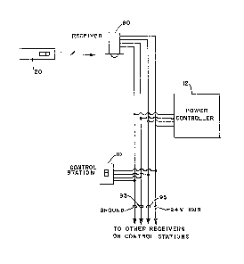
In the drawin~s, wherein like r~ference numeral~ denote
like parts, the remote wireleqs, load control system of the
present invention i~ described in Fig. 1. The latter
includes transmitter 20, typically an infrared tran~mitter,
and a r~ceiver 60 therefor. The embodiment of Fiy. 1 also
includes control ~tation 10 and power controller 12.
Control s-tation 10, receiver 60 and power controller 12 are
linked together typically by a four-wire bus, the latter
consisting, for example, of a ~24Vrms line, a ground line,
analog signal line 93 and take command line 95.
~3~.~33~
As described in Fig. 2A, tran-~mitter 20 lncludes DC
power ~ource 24, typically a nine volt battery, connected
betwPen tran~mit~er ground and one 3ide of ~witch 26. The
latter i~ preferably a normally open, sin~le-pole, ~ingle
throw (SPST) momentary puYhbutton-type switch that, when
closed/ serves to connect power source 24 to power supply
circuit 28. Power supply circuit 28 is included to provide a
stable, regulated volta~e source and can be readily
implemented in the ~orm o~ a LM 2931Z inte~rated circuit
manufactured by National Semico}lductor Corporatlon.
Power output line 30 from power ~upply cîrcuit 28 i9
connected to one end of resi~tive impedance 32 of slide-
operated potentiometer 34, the other end of impedance 32
being coupled to ground. Power line 30 is also connected to
provide the re~uisite power input to analog-to-digital
converter 36, digital encoder 38, carrier fre~uency
oscillator 46 and amplifier 48. ~ach o~ these latter devices
is also connected to transmitter ground.
Analog-to-digital converter 36, typically a commercially
available integrated circuit such a~ ADC0804 of National
5emlconductor ~orporation, is provided for converting an
analo~ si~nal into a parallel digital output. To this end,
analog input terminal 40 o~ convert~r 36 is connccted to
manually operable wiper 42 o~ potentiometer 34, wiper 42
being a conventlonal potentiometer wiper, conflgured to move
typically lin~arly or along a curved path of operation in
contact with resistive impedance 32. Adjustment of wiper 42
varies the resi~tive imp~dance of potentiome-ter 34 over a
continuum of values. Parallel output digital databus 44 of
converter 36 is connected as the data input to encoder 3B,
the latter typically being a commercially available
integrated circuit such as MC145026 of Motorola Corporation
that produces serially encoded data. The data output
termlnal of encoder 38 is connected to the data input
terminal of carrier frequency oscillator circuit 46, the
t~ 3 3 ~
latter being exemplified in an ICM~556 integrated circuit
manufactured by ~n~ersil, Inc., Cupertino, California.
The output of oscillator circuit 46 is connected to the
cathode of the first of a pair of series-connected infrared
light-emittin~ diodes 50 and 52 through amplifier 48. The
anode of diode 52 i5 connected to the positive terminal of
power source 24. By mounting switch 26 on the actuator of
potentiometer wiper 42, the transmitter can be operated in
two different modes, track and preset, as detailed
hereinafter.
In an alternative form of the transmitter of the present
invention, as shown in Fig. 2B, switch 26 is omitted and
power supply ~4 is connected to the input of power supply
circuit 28 through a pair of parallel, normally open,
single-pole, single-throw spring-loaded pushbutton momentary
close switches 54 and 56. The latter are mechanically
coupled, as indicated by the dotted line, to wiper 42 so
that one of the switches is momentarily closed while the
wiper is being moved in one direction, the other switch
being mo~entarily closed while the wiper is moved in the
opposite direction. Thus, motion of the wiper in either
direction closes one or the other of the two switches,
energizing power supply 28 an~ providing the requisite or
desired analog signal to A/D converter 36. Details of a
switching mechani~m particularly userlll as ~witches 54 and
56 are disclosed in U.S. Patent 4,689,547.
Receiver 60, as shown in Fig. 3, i9 de~igned to be
contained in a housing typically adapted for mounting in or
on a wall (not illustrated) or ln or on a ceillng (See Fig.
9A), but can be free standing i~ desired or adapted to be
mounted as a part of the power controller circu.it.
Receiver 60 includes power supply circuit 62 having its
input coupled to a sourGe of 2~Vrms. Outputs of 2~V~C, 5.6V
~31e9~
DC (regula~ed~ and 5.0V DC (unregulatecl~ are prov.ided. The
24VDC output of power supply circuit 62 is coupled a~ a
power input to take/relînquish command circult 90. The 5.6V
DC output of power supply circuit 62 is coupled/ a~ a power
.input, to decoder circuit 84. The 5.0V DC output of power
supply circuit 62 i~ coupled, as a pow~r input, to
amplifi~r/demodulator clrcuit 80A/80B and recelver diode and
tuned filter circuit 82.
Infrared signals are received by a receiver diode or
diodes and selected by using a tuned circuit in receiver
diode and tuned fi~ter circuit 82. The output of the
recei.ver diode is a serial cligital signal modulating a
carrier. It i5 cunnected to the input of amplifier circuit
80A, the output of ampliier circuit 80A being connected to
the input to demodulator circuit 80B. The output of
demodulator circuit 80B is a serial digital si~nal that is
connected to the sicJnal input terminal of decoder circuit
84. Amplifier circuit 80A and demodulator circuit 80B may
be implementecl by using a TDA 8047 integrated circuit, a~
manufactured by 5ignetics.
The receiver diode is preferably mounted on or in the
wall or ceiling mounted housin~ in such a manner that it can
receive sicJnal~ from the widest possible number of
directions.
Decoder circuit 84 is provided for converting a serial
digital si~nal at it~ signal input terminal to a parallel
digital signal on signal output bus 86 and al50 to signal
the Take/Reli~qui~h command circuitry that a valid signal
transmission has occurred. A suitable circuit i5
30 commarcially available as an MC 145029 chip manu~actured by
Motorola. Output bus 86 is connected to the signal input
terminals of digital-to-analog converter circuit 88. Valid
transmission output line 91 is connected to a control input
of take/relinquish command circuit 90. The 5ignal output
terminal of digital-to~analog converter circuit as i~
~ 3 L_ ~ ~J~ ~
connected to a switch means in take/relinquisll command
circuit 90. When the valid transmission output æignal on
line 91 goes high, the switch means closes and the analog
output signal appears on output line 93. Take command line
95 iR connected to a second corltrol input of take/relinquish
command circuit 90. When the signal on this line ~oes low,
the switch means in take/relinquish command circuit ~0 opens
and the analo~ output signal i9 removed from output line 93.
In operation of the transmitter of F.ig. 2A, when switch
26 is closed, the transmitter circuit i5 powered by source
24, at least during the time that switch 26 remains
depressed. Durin~ that time, the analog signal provided by
the position of wiper 42 in potentiometer 34 is sampled by
A/D converter 40 and converted into digital signals in the
form of parallel bits available on bus 4~. ~ncoder 38
serves to encode the parallel bits of the digital signal
into a sinyle line, se.rial-encoded data signal, thereby
conferrin~ relative noise immunity for decodin~ at the
receiver side. The serial-encoded data signal iæ ~ed into
oscillator 46 to provlde amplitude modulation of the carrier
frequency generated by the oscillator. Such modulation is
intended to provide a high signal-to-noise ratio for
infrared detection on the receive:r side as will be described
hereinafter. The duty cycle of the carrier frequency
oscillations is approximately 20% to reduce power
consumption. The amplitude mod~lated signal from oscillator
46 is then amplified in amplifier 48 to power infrared
light~emitting diodes 50 and 52. It should be apparent to
those skilled in the art that the integrated circuit chips
and the modulation scheme selected insure very low power
consumption, and that other integrated circuits and
modulation schemes may also be utilized.
The cixcuit of Fig. 2~ can be used in two different
modes. In a first mode, referred to aæ tracking mode, one
3r~ simply holds switch 26 down and adjusts the setting of wiper
ll
42 on pQtentiometer 34~ The lighting level con~equently
provided, as wlll be apparent hereinaf ter, w.ill vary
p:roportionately as the potentiometer is adjllsted glvlng
control over the power fed to the load substantially
instantaneously in accordanoe with the position of the
slider relative to resistive lmpedance 32. In an
alternative mode, re~erred to as preset mode, one can :~irst
adjust the potentiometer and then mom~ntarily close switch
26. CLosure of switch 26 then e~fectively instantly ad~usts
the power flow to the load at a level indicated by the
position at which the potentiometer was set.
An infrared signal ~rom transmitter 20, when recelved by
inf.rared receiver d:iode 82, is converted to an electrical
signal by the dlode and applied to the input of pr~-
amplifier circuit ~0. The latte~ selects the signal at thedesired carrier frequency, amplitude demodulates to strip
the carrier frequency, and amplifies the demodulated signal
to obtain the serial-encoded signal sent by t~ansmltter 20.
The serial-encoded signal is then applied to the input of
decoder 84. To ensure that the data to bc decoded are
valid, decoder circuit 84 pre~erably includes, in known
manner, timing elements preset to match the timin~ of the
serial-encoded data transmitted from diodes 50 and 52. When
two consecutive valid data words iare received from pre-
amplifier ~0, decoder circuit 84 provides a decode enablesi~nal and applies it to line 91. Additionally, the decoder
output which is a parallel bit digital ~ignal, is latched
internally and provided to bus 86. That parallel signal i5
then converted in D/A converter circuit 88 int~ an analog
signal applied to one of the signal input o~ switch means
90. Because the decoder output is latched, the D/A
conversion need not be synchronous.
Applica-tion o~ an enable signal on line 9l resets the
state o~ the switches in switch ;neans 90 so that the output
~rom D/A converter circuit 38 is connected to analog signal
12
line 93 of switch means 90.
The enable signal on line 91 can also be used to drive a
signal received indicator light, ~hich i,5 especially useful
when the load under control is remote from the receiver.
The operation of the transmitter of Fig. 2B is ~imilar
to the operation of the transmitter o~ ~.ig. 2A in it~
'track' mode. The di~ference ls that either switch 54 or
switch 56 is closed automatically as the wiper 42 is moved
and hence t.he operator of the ~ystem merely has to move the
wiper 42 in the desired direction to send the appr~priate
signal; there is no necessity to operate overtly another
switch.
The embodiment of transmitter 20 illustrated
schematically in Fig. 4 include D.C. power sourc~ 24,
connected between system ground and the ano~e of protection
diode 304. The cathode of diode 304 is connected to the
emitter of transistor 301. Capacitor 302 is connected in
parallel with power source 24 and diode 304. The collector
of transistor 301 i8 connected to the input terminal o~
volta~e regulator 306. The base s~f transistor 301 i~
connecte~ through re~istor 305 to the collector of
transistor 303, and the emitter o~ the latter is connected
to ground. The base o~ transistor 303 is connected to
respective terminals of resistor 308 and resistor 310. The
other términal of resistor 308 i5 grounded and the other
term.inal of resistor 310 i5 connected to one ter~inal of
capacitor 30~ and of switches 54 and 56. The other
terminals of ~witches 54 a~d 56 are connected to the emltter
of transis~or 301, The other terminal of capacitor 307 i5
connected to the collector of tran~istor 301. The reference
terminal of voltage re~ulator 306 is connected to ground.
The output terminal of voltage regulator 306 is ccnnected to
power output line 30. Capacitor 312 is connected between
power output line 30 and ground.
Power output line 30 is connected to one end o~
~3~3~
13
resistive impeclance 32 of slide-operated potentiometer 34,
the other end of resistive lmpeclance 32 b0:Lng connected to
ground. Power output line 30 is al50 connected to p.in 16 of
digital encoder circ~it 328, to pin 20 of analog-to-di~ltal
converter circu.it 330 and to pin 14 of 05cillator circuit
342.
Manually operable wiper 42 of potentio3neter 34 is
connected tc the voltage input terminal at pin 6 of analog-
to-digital converter circuit 330. Resistnr 314 is connected
between CLK R input a-t pin 19 and CLK IN input at pin 4 of
converter circuit 330. Timing capacitor 316 i5 connected
between CLK IN input pin 4 of converter circuit 330 and
ground. CS at pin 1, RD at pln 2, VIN(-) at pln ~, A GND at
pin 8 and D GND at pin 10 of convertor circuit 330 are all
connected to ground. The data output connections at pins 11,
12, 13, 1~ and 15 of converter 330 are connected to data
input connections at pins 5, 6, ~, 9 and 10 of encoder
circuit 328 respectively. The interrupt request INTR output
at pin 5 of converter 330 is connected to transmit-enable
input TR at pin 1~ of encoder 328. The write request WR
input at pin 3 of converter 330 i~ connected to the output
at pin 5 of oscillator 342.
Timing circuit capacitor 324 is connected between CTC
connection at pin 12 of encoder 328 and the common junction
of resistor 322, timing rQsistor 326 and ground. The othex
end of resistor 32~ i~ connected to RS connection at pin 11
o~ encoder 328 and the other end of timing resi~tor 326 is
connected to RTC connection pin 13 of encoder 328. Pins 3,4
and 8 of encoder 328 are connected to ground. The output at
pin 15 of encoder 328 is connected to R~S at pin 10 of
carrier frequency oscillator 342.
Resistor 320 i~ connected ~etween power output line 30
and the di~charge connection pin 13 of oscillator 342. The
anode of diode 344 is connected to pin 13 of oscillator 324.
The cathode of diode 344 and one e~d of resistor 348 are
3 ~
1 .~
connected to -the threshold (THRE:S) input at pin 12 o:f
o~cillator 342. The other end of resistor 348 is connected
to pin 13 o~ oscillcltor 342. Threshc)ld input pin 12 is
~ur-ther connected to trigger input pin 8 of oscillator 342,
and one end of tim.ing capacitor 350. The other end of
timing capacitor 350 being connected to ground. The output
at pin 3 o~ oscillator 342 is connectecl to respective one
ends of re~istors 3~2 and 353.
A samplin~ frequency oscillator forms part of oscillator
342. Timing capacitor 340 is connected between trigger
input pin 6 of oscillatcr 342 and ground. Trig~er input
TRIG at pin 6 is further connected to the threshold input
THRES at pln 2 of o~cillator 342. Timing resistor 333 is
connected between pin 2 and output pin 5 of oscillator 342.
Pin 6 o~ oscillator 342 is connected to the anode o~
protection diode 356, the cathode oP the latter be.in~
connected to power output line 30. Power on reset capacitor
33~ is connected between ground and reset input RES at pin 4
of oscillator 342~ Power on timing resistor 318 i5
connected between pin 4 of oscillator 342 and power output
line 30. Pin 4 of oscillator 342 i5 connected to the anode
of protection diode 354, the cathode of the latter being
connected to power output line 30.
The other side o~ rssistor 352 i~ connected to the base
o~ transistor 36. The emitter o~ transistor 35 i8 connected
to ground, the collector of trans1stor 35 being connected to
the cathode of infrared li~ht emitting diode 50. The anode
of in~rared light emlttlng diode 50 is connected to the
cathode of infrared light emitting diode 52, the anode of
the latter being connected to the cathode of diode 304
through re~istor 354.
S.imilarly, the other side of resistor 353 i~ co.nnected
to the base of transistor 36. The ~m.itter of transistor 36
i5 connected to ground, the collector of transistor 36 bein~
Gonnect~d to the cathode of infrared light emit~ing diode
~ 3 ~
51. The anode o~ infrared light emitting dlode 61 is
connected to the cathode of infrared light emitting diode
53, the anode ol the latter being connected to the cathode
of diode 304 through .resistor 356.
The operation of the transmitter o~ Fig. 4 is as
follows. On ~irst inserting power source 24 into the
transmitter and making eonnection to it, po~er ~upply
capacitor 302 is charged up through protection diode 304.
Power supply capacitor 302 serves to provide peak pul~e
currents to infrared light emitting diodes 50, 51, 52 and
53. Protection diode 304 prevents discharge o~ power source
24 and damage to transmitter Gircuitry in the event the
power source 24 is mlswired.
Moving wiper 42 o~ potentiometer 34 cause~ either switch
54 or swi~ch 5~ to close. This in turn causes transistor
303 to turn on, ~ollowed by transistor 301 connecting power
source 24 to voltage regulator 306 through protection diode
304 and translstor 301. In the preferred embodimen-t, the
output voltage of regulator 306 is approximately 5V.
Capacitor 312 filters the output volta~e on power output
line 30, which is used to power the other circuit
components.
Transistors 301 and 305 together with capacitor 307 and
resistors 305, 308 and 310 form a "nagger" circuit that
~ntinues to provide voltage to regulator 306 for a short
period of time after switches 54 or 56 ar~ opened, henc~
enabling transmission to be complete~ with a stable slgnal
from wiper 42. When switch 54 or switch 56 i opened,
capacitor 30~ keeps transistor 303 turned on until it is
charged up thro~gh resistors 310 and 303, at which time
transistors 303 and 301 turn o~ and capacitor 30~ agaln
discharges.
Wiper 42 of potentiometer 3~ taps oPf an analog voltage
from resistive element 32. This analog voltage is applied
to the input terminal o~ analog~to-di~ital converter 330.
16
Re~istor 31~ and capac.itor 316 are external components o~ an
.internal clock circuit within analog--to-di~ita1 converter
33C. Once the convers.ion process i5 completed, the digital
output is latched onto pins 1l, 12, 13, 14 and 15 of
converter 330 and the INTR output on pin 5 i5 driven low.
This transition is applied to the transm.it-enable input pin
l4 of encoder circuit 323 causing the encoder clrcuit to
begin the encoding process using the data available at its
input pins 5, 6, ~, 9 and lO. Resistors 322 and 3~6 and
capacitor 3~4 are external components o~ an internal clock
circuit within encoder circuit 328. The serially encoded
output of encoder 328 appears at pin l~ which is connected
to the RES input at pin lO of oscillator 342.
Oscillator 342 is actually two oscillators. The first
is a carrier frequency oscillator with connections at pins
8, 9, lO, l2 and 13. Capacitor 350, resistors 320 and 348,
and diode 344 are timing components of the carrier frequency
oscillator which serve to generate a high frequency ~in the
pre~erred embodiment lO3 kHz) carrier but with a duty cycle
of only 20~ to reduce power consumption. The low duty cycle
is achieved by the arranyement of resist4r 348 and diode
344. The carrier frequency oscillations are output at pin 9
and are modulated by the serially encoded data stream
appll~d to pin lO.
The second oscillator is used to con-trol the sampling
rate of analog-to-digital converter 330 and ha~ connections
at pins 2, 4, 5 and 6. Resistor 333 and capacitor 340
determine t~e output frequency on pin 5 (which in the
pre~erred embodiment i~ 20 ~). Diode 356 resets capacitor
30 340 when lin~ 30 goes low at power off.
~hen switch 54 or 56 is ~lrst closed, the input to RES
at pin 4 is low and prevents the second oscillator from
functionirlg. This inpu-t volta~e will rise as capac:ltor 334
is charged throu~h resistor 318. Once ~h~ voltage rises
a~ove a thresho.ld value the 4scillator begins oscillating.
5~
17
In this manner~ the oscillator is not gated on until any
noise associated with the power up transition hRS died away.
Diode 354 resets capacitor 334 when l.ine 30 goes low at
power off. The output ~rom pin 5 o~ oscillator 342 i5
appl:ied to the WR input at pin 3 of analog-to-digitc
conver-ter 330 and hence controls the samplin~ rate.
The modulated output of carrier ~requency oscillator 342
appears at pin 9 and is applied through resistor 352 to
transistor 35 and through re~istor 353 to transistor 36.
The modul~ted output is amplified by transistors 36 and 36
an~ modulates the current flowing in infrared light-emitting
diodes 50, 51, 52 and 53 to produce properly modulated
infrared siynals at the carrier frequency. Four light-
emitting diodes are u~ed to increase the range of the
transmitter.
The presently preferred v~lues of the resistors and
capacitors of the embodiment of Fi~. 4 ar~ set forth in
Table I below.
TABLE I
VALUE
_SISTOR IN OHMS ~OLERANCE
34 250K(VA~)
305 lOK 5~
308 68K 5%
310 lOOK 5%
314 6.8K 5~
31~ lOOK 5%
320 1.5K 5%
322 39~ 5~
32~ 18.2K 1%
3 ~
1~
338 1.5M 5%
~48 2~.4K 1~
352 1~ 5%
353 15~ 5%
35~ 1 5
356 1 5~
CAPACITORVALUE TOLERANCE
302 1500uF 20%
307 luP 10%
312 lOOu~ 10
31~ 220pF 10
324 ~.~nF 10%
334 lOOnF 10%
340 2~n~ 10%
350 22ClpF 196
In the preferred embodlment, the ~ollowing components
are employed. Diode 304 is a type lN5817, diodes 344, 354
- and 356 are all type lN914. Infrared li~ht-emitti~g diod~
50, 51, 52 and 53 are type SFH484. Tra~sistors 35 and 36
are MPS A2~. Transistor 301 is an 2N5806, transistor 303 is
a 2N4123. VoI~age regulator 30~ is a National ~emicondustor
LM 29312. Analog-to-digital converter 330 ls a National
Semiconductor ADC0804. Encoder circuit 328 is a Motor~la
MC145026. Oscillator 3~2 i an Intersil ICM~556. Power
sourcej24 is a 9V battery, Switche~ 54 and 56 can be any
momentary contact switches, rated for dry circuit use, that
can be coupled to potentiolrle ter 34 .
Skilled practitioners will appreciate that the
inte~rated circuit chips and oth~r components havin~
~omewhat dif~erent operating parameters may also be
satisfactorily employed in the transmitter. Also it will be
3 ~
19
appreciated that the movement of wiper 42 can be detected
electronically or optically instead o~ mechanically a~ by
using switches 54 and 56.
The receiver embodiment illustrated ~chematically in
Fig. 5 is the pre~ently preferred embodiment of the receiver
block-diagrammed in Fig. 3. Power supply 62 comprises diQde
402, PTC re~i~tor 401 resistor~ 404 and 410, zener diodes
403 and 406 and capacitor 408. The positive terminal o~ the
24Vrms supply i9 connected to the anode of diode 402, the
cathode being connected ~o one terminal o~ PTC resi~tor 401.
The other terminal of PTC resistor 401 is connected to the
cathode of zener diode 403, ~o one terminal of capacitor
408, and the V+ output of the power supply. The anode of
zener diode 403 and the other terminal of capacitor 408 are
connected to ground. The cathode of zener diode 403 is
connected to one terminal of resi~tor 404. The other
terminal of resistor 404 is connected in common to the
cathode of zener diode 406, one terminal of re~ister 410 and
the 5V output of the power ~upply. The anode of zener diode
406 is connected to ground. The other terminal of resistor
410 is connected to the cathode of receiver diode 412. The
24V DC output of the power supply is connected to the anode
o~ diode 44~. The V~ output of t'he power supply is also
connected to the cathode of diodes 468 and 4~8, to one
terminal of relay coils 480 and 432 in take/relinquish
command circuit 90, to the cathode of diode 411 and to the
positive supply terminal of IC40~. The 5.0V output of the
power supply is co~ected to the VDD terminal o~ decoder
integrated circuit 438, to the positive ~upply terminal of
ampli~ier/demodulator integrated circuit 424, to the supply
terminal of timer 423, to one terminal of relay contact 449
and through capacitor 436 to ground.
Receiver diode and tuned filter circuit 82 comprise
receiver dlode 412, variable inductor 414, and capacitors
416 and 418. The cathode o~ receiver diode 412 i~ connected
to the 5.0V output of power supply 62 through resistor 410.
The arlode of receive.r cliode 4l2 is connected to one terminal
of variable inductor 414, to one terminal of capac:itor 416
and to the input lim:lter terminal oP amplifier/ demodulator
circuit 424. The other terminal of variable inductor 414 is
connected to ground. The other terminal of capacitor 416 i5
connected to one terminal oÇ capacitor 41a. The other
terminal of capacitor 418 i8 connected to ~round. The
~unction between capacitors 416 and 418 is connected to the
controlled high frequency amplifîer and Q-~actor ki:Ller
within amplifier/demodulator integrated circuit 424.
Amplifier/demodulator 80A/80B comprises
amplifier/demodulator integrated circuit 42g, capacitors
420, 422, 426, 428, 430 and 434 and inductor 432.
Cap~citors 4~0 and 4~2 are stabilization capacitors
connected to the controlled high fre~uency amplifier within
ampli~ier/demodulator integrated circuit 424. Capacitor 426
is a couplin~ capacitor connected to the controlled high
frequency amplifier within amplifier/demodulator intPgrated
circuit 424. Capacitor 428 is connected to the automa-tic
gain control detector within ampli~ier/demodula~or
integra-ted circuit 424 and controls the acquisition time oP
the automatic gain control detector. Capacitor 430 is
conneçted to the pulse shaper circuit within
ampli~ier/d~modulator intagrated circult 42g and controls
its time con~tant. Capacitor 434 and inductor 432 are
connected in parallel and are connected to the reference
ampli.fier circuit within amplifi~r/demodulator circui-t ~24.
The output of the ampli~ier/demodulator integrated circuit
30 i5 connected to the input to decoder integrated circuit 438.
Decoder circuit 84 comprises decoder integrated circuit
438, resistors 442 and 4S6, and capacitors 440 and 454. The
VSS terminal of decoder integrated circuit 438 is connected
to ground. As noted above, the VDD t~rminal of decoder
integrated circuit 438 i8 connected to the 5V output of
21
power supply 62. Resistor 442 i~ connected to the pulse
discximinator pins of decoder integrated circult 43~.
Capacitor 440 is connected between one of the pulse
discrim.inator pi.ns and yround. Together, resi.stor 442 and
capacitor 440 set a time constant that is u e~ to determine
whether a wide or a narrow pulse has been encoded. Resi~tQr
456 is conn~c~d in parallel with capacitor 45~, and the
parallel combination is connectecl between the dead time
discriminator p~n of decoder inte~rated clrcuit 438 and
ground. These components set a time constant that i5 used
to determine both the end of an encoded word and the end of
transmission. The decoded data appears at the data output~
of decoder integrate~ circuit 438. Pins 1, 3 and 4 of
decoder integrated circuit ~38 are connected to ground.
Digital-to-analog convertor circuit 88 comprises
resistor~ 444, 446, 448, 450 and 452. Each data output o~
decoder integrated circuit 438 is connected to a terminal of
one of these re~istors. The other terminal of ~ach resistor
is connectad to the positive input of integrated circuit 40
in take/relinquish command circu.it gO. The resistor values
are selected such the the data word on the data output
terminal~ of decoder integrated circuit 438 i5 converted to
an analog voltage on the positive input terminal of
inte~rated circuit 40~.
Takejrelinquish command circuit 90 comprises resistors
405, go~, 460, 466 ancl 472, capaci~or 462, diodes 411, 413,
453, 464, 468, 470 and 47~, transistors 474 and 476, relay
coils 480 and 482, relay contacts 449 and 484, and
integrated circuit 407. The valid transmission output
terminal o~ decoder integrated circuit 438 is connected to
the anode of diode 458 via line 91. The cathode of diode
458 is connected to one terminal o~ resistor 460 to one
terminal of contacts 449 and to one terminal of capacitor
462. The remaining terminal of re~istor 460 is connected to
ground. The remaining terminal of contacts 449 ls connected
1 3 ~
22
to a ~5V power supply~ The remaining terminal of capacitor
462 is connected to the cathode of diode 464 and one
terminal of resistor 466. The anode of diode 464 is
connected to ground. The other terminal of resistor 456 is
connected to the base o~ transistor 4~4. The emitter of
transis~or ~4 is connected to ground and the collec~or is
connected to one terminal of resistor 451. The other
terminal of resistor 451 is conneoted to the cathode of
diode 470, one terminal of resistor 4~2, one terminal of
relay coil 480 and the anode of diode 468.
The other terminal of resistor 472 is connected to the
base of transistor 4-~6. The anode of diode 470 is connected
to the emitter of transistor 476 and to take command line
95. The collector of transistor 4~6 is connected to one
terminal of relay coil 482 and to the anode of diode 478.
The cathodes of diodes 46~ and 478 and the other terminals
of relay coils ~80 and g82 are connected to the V+ output of
power supply 62. The negative input of in~egrated circuit
40~ is connected to one terminal of resistor 405 and 409.
The other termi~al of resistor 405 i~s connected to ground.
The other terminal of resistor 409 is connected to the
output o~ integrated circuit 4G~, the anode o~ diode 411,
the cathode of diode 413 and one terminal of relay contact
~84. The cathode of diode 411 is connected to V~. The
anod~ of diode 413 is connected to ground. The free
terminal of relay contact 484 i5 connected to analog signal
line 93.
Receiver 60 further includes light-emitting diode 427
and driving circuits comprising timer circuit ~23,
3Q transistors ~29 and 439 and associated component~. Light-
emittin~ diode 42? indicates whether power to the load is on
or off and whether the receiver is receiving a signal, as is
described in more detail in Canadian copending
application serial number 565,219 filed April 27, 1988.
Pins l (RESET), 10, 11, 12, 13 and 14 of timer circuit
1 3~ ?
23
423 are connected to the 5.0V supply. Pin 7 i~ connected to~round. The Q OUtpllt ~ pin 6) i~ connected to the D input
(pin 2). The valid transmi~sion output VT, l:lne 9:l, from
decoder inte~rated circuit 438 is connected to the CLK input
(p.in 3) of t.imer circuit ~3 ancl to the ~nocle o~ d.iode 4~9.
The cathode oE diode 419 is connected to one terminal of
capac.ito.r 415, and to corre~pondîng terminals of re~istors
417 ~nd 421. The other terminals of capacitor 415 and
resi~tor 417 are connected to ground. The other terminal of
resistor 421 i5 connected to the SET input Ipin 4) of timer
circuit 423. The Q output ~pin 5) of timer cir~uit 423 i5
connected to one terminal of resistor 425.
The other terminal of resistor 425 is connected to the
base of transistor 429. The emitter of transistor 429 is
oonnected to ground. The collector o~ transistor 429 is
connected to the cathode of light-emltting diode 427. The
anode of light-emitting diode ~27 i~ connected to the
cathode of zener diode ~31, to the anode of zener diode 433,
and to one terminal of resi~tor 435. The anode of zener
diode 431 i~ connected to ground. The other terminal of
resistor 435 is connected to the collector of transistor 439
and one terminal of resistor 437. The other terminal oE
resistor 437 is co~nected in common to the emitter of
transistor 43~, the cathode of diode 441 and the anode o~
25 ~ener diode ~43. The cathode of zener diode 443 i5
connected to the cathode of zener diode 433 and one terminal
of PTC resistor 4~5. The other terminal of PTC resistor 445
is connected to the cathode o~ diode 447, the anode of diode
447 being connected to the -~24V full wave supply.
The anode of diode 441 is connected to the base of
translstor 439 and one terminal of resistor 453. The other
terminal of resistor 453 is connected to the relay on/o~
line 550 in power controller 1~. When the relay is on, line
550 is held close to ground. ~hen the relay i5 off, line 550
floats to -~24V.
3 ~ ~
2~
In~rared receiver diode 412 r~ceiv~s infrared signals
which are se1ected by the tuned circuit ~ormed by varlable
inductor 414 and capacitors 416 and 418. The selected signal
i5 then appl.ied to the input o~ ampli~i~er~demodulator
inteyrated circuit 4~4. The amplified and demodulated
output signal .is applied to the input of decoder integrated
circuit 438. The digital output produced i8 converted to an
analog signal by resistors 444, 446, 448, 450 and 452, and
applied to the positive input of integrated circwit 40~
which acts as a buffer amplifier. The output of integrated
circuit 40~ is applied to one terminal of relay contact 484.
Diodes 411 and 413 serve to clamp the output voltage from
integrated circuit 407 to be no greater the V+ or less than
ground.
Wh~en a valid output i~ available at the digital output
terminals of decoder integratPd circuit 438, then line 91
goes high. This causes the voltage on the cathode of diode
464 to go high and transistor 4~ to turn on, and allows
current to flow through relay coil 480, closing relay
contacts 4~9 and 484 and applying the analog output ~ignal
to line 93. Capacitor 4,62 then charges through resistor 4~6.
When line 91 goes law, capac1tor 462 i5 kept charged at -~5V
by contacts 449 which remain clos~ed as do Gontact~ 484 since
they are contacts of a latching rlelay. Dlode 464 protects
the base-emitt~r junction of tran istor 4~4.
If take-command line 9~ yoes low then transistor ~76 is
turned on and receives base current through relay coil 480
and resistor 472. Collector current flows through relay
coll 482 a~d cau es relay contact~ 449 and 48~ to open.
30 This causes capacitor 462 to discharge through resistor 460,
with the discharge current flowing through diode 464.
Tra~sistor 4~4 is turned o~f and the energy stored in relay
coll 480 circulate~ through protection diode 46~. Diode 45
protects the output terminal of decoder integrated clrcuit
~38.
13~ ~3~ ~
~5
Take-com~and line 95, going high, causes transistor 476
to turn off and the energy stored in relay coil 482
circulates through protection diode 478. Diode 4~0 allows
take command line 9S to be pulled low when translstor 474
turns on thus relinquishing col~mand at all other connected
stations.
The operation of th~ Gircuitry that drives light-
emitting diode 427 is as follows. In the ab~ence of a
received signal, the Q outpu-t of timer circuit 423 is hlgh
and transistor ~29 is on. If ~he load is also on, then the
on/off input i5 low and trans.istor 43g is also on. Hence, a
relatively lar~ amount of current flows through li~ht-
emitting diode 42~ and the latter glows brightly, indicating
that the load i5 on.
V~ (l.ine ~1) goes high each time a valid txansmission
(i.e. with a frequency of 20Hæ) is received by the receiver.
Timer circuit 423 is set up as a divide-by-2 courlter so that
the Q output (pin 6) osoillates at a frequency of lOHz. This
causes transistor 427 to turn on and off at that frequency
so that light-emittin~ diode 427 blinks at ~he lOHz
frequency, indicating the reception of a s.ignal from the
tran~smitter.
When valid transmission.~ are no longer received, the Q
output goe.s high, turning transistor 427 on once again. If
the resul-t of the transmission was to turn the load off,
then the on/off input is high and tr~nsistor 439 is now off.
The current ~lowing through light-emitting diode 42~ also
has to flow thro~gh resistos 437, and it is a much lesser
value than previously~ Hence light-emitting diode 427 glows
more dimly, indicating that the load is off.
The varlous diodes and zener diodes are for the
protection of transistors 429 and 439.
The presently preferred values of resistors and
capacitors for the circuit of Fig. 5 are given ln Table II
below. All resistors are 0.5W power rating unless otherwise
~3~33~
26
stated.
TABLE II
VALUE
RESISTOR IN OHMS CAP~CITOR VALUE
404 3.3k 408 lOOuF
405 lOk 415 luF
409 30.lk 416 150pF
410 22 41a 680pF
417 lM 420 3.3nF
421 lk 422 22nF
425 15k 426 lnF
435 810 428 47nF
437 43k 430 330pF
442 33k 434 lOOOpF
444 20k 436 22~F
446 40k 440 lOnF
4~8 80k 454 lOnF
450 lOk 462 2.2uF
451 68
452 160k
453 33k
45~ 645k
460 lM
466 56
4~2 56~
PCT resist~rs 401 and 445 are preferably 180 ohms.
Light-emitting diode 427 is preferably a Martec 530 O.
Diodes 419, 458, 464, 468, 4~0 and 478 are preferably
type lN 914. Diodes 402, 411, 413, 441 and 447 are
preferably type lN 4004. Zener diode ~03 is a type 1.5 KE
39A. Zener diode 406 preferably has a zener voltage of
5.0V. Zener diodes 341 and 433 preferably have zener
* Trademark
3 ~ ~
voltages o~ 33V. Zener diode 443 preferably has a zener
voltage of lOV. Receiver ~io~e 412 is pre~erably a Siemens
type SFH205. Transistors 429, 474 and 476 are preferably
type MPSA29. Transistor 439 is preferably a type MPS 1992.
5 Amplifier/demodulato~ integrated circuit 424 is preferably a
Signetics*type TDA 304~. Decoder integrated circuit 438 i5
preferably a Motorola type MC 145029. Integrated circuit
407 is preferably a Motorola type MC 33172P. Timer circuit
423 is preferably a 74EIC74. Variable inductor 414
10 preferably has a maximum value of 18m~. Inductor 432
preferably has a maximum value of 4mH. Relay coils 480 and
482 and relay contacts 449 and 484 together form a latching
type relay, ~or example an Omron G5AK237POC24.
As shown in Fig. 6, the power controller of the present
invention receiveC signals from the receiver or another
control station and outputs a phase-controlled output
voltage. To this end, flip~flop circuit 500 i5 connected to
power-up preset potentiometer 544, analog signal line 93 and
take-command line 95. Its ou~put is connected to phase
modulation circuit 502, and it receives power from a D.C.
supply. On first powering up the power controller, ~lip-
flop cirouit 500 assumes a state where the voltage tapped
off power-up preset potentiometer 5~4 is applied to phase
modulation circuit 502. When take-command line 95 i5 pulled
low, flip-flop circuit 500 to~gles, and the voltage on
analog si~nal line 93 is applied to phase modulation circuit
502.
Pha~e modulation circuit 502 has outputs to relay 52B,
on/off control line 550 and optocoupler 50~. If the voltage
at the input to phase modulation circuit 502 is above a
predetermined value, then voltage is applied to the coil o~
relay 528 causing its contact3 to close, applying the
voltage to main triac 532. Varying the input voltage to
phase modulation circuit 502 above the predetermined value,
produces an output signal o~ varying phase delay from the
* Trademark
~3~L~3~
28
zero crossings of the A.C. line, which signal is applied to
optocoup].er 504. Phase modulation circuit 502 i5 powered
from transformer 510.
The output from optocoupler 504 i8 applied to slg~al
triac 514, gating the latter on. Resistors 5~2, 524 and ~26
limit the curr~nt throuyh triac 514 in the on state.
Resls~or 508 and capacitor 512 form an RC snubher for triac
514. Resistor 506 limit~ current in optocoupler 504.
Capacitor 520 charges to a voltage limited by ~ener diodes
516 and 51~ when triac 514 is in the o~f state. When signal
triac 614 is gate~ on, capacitor 520 discharges and cau~es a
pulse of current to flow through pulse trans~ormer 530.
The pulse of current ~enerated on the secondary side of
pulse trans~ormer 530, Plows through ~a-te resistor 5~8 and
gates on main triac 532. Resi~tor 534 and capacitors 536
and 538 form a snubber ~or main triac 532. Inductor 540 and
capacitor 542 form a radio frequency interference filter.
Thus, the output voltage from the power controller is
phase-controlled A.C. volta~e whose value depends on the
voltage on analog signal line 93. In the event this voltage
is adjusted to be below a certain predetermined value, then
power relay 52~ will open to provide a po~itlve air gap
between the power source and the output. On restoration of
power ~ollowing a power failure, the output voltage will
depend on the setting of pow~r preset pote~tiomcter ~4g.
A suitable control ~tation 10, for use with the power
controller described in Fig. ~, is shown in block dia~ram
form ln Fig. ~A, and compri~es power supply 600,
potentiometer~take command switch ~1rcuit 602 and
take/relinquish command circuit 604. Power supply 600 has
as its input, a sQurce of 24 Vrms full wave recti~ied direct
current, and outputs a regulated 5.6V to potentiometer/take
command switch circuit 602. The outputs from
potentiometeri-take command switch circuit 602 are an analog
.35 signal voltage and a take-command signal. These are
13~ ~33~
29
connected to take/relin~uish command circuit 604.
Take/rellnqu.ish command circuit 604 .i~ connected to analog
signal bus 93 and take command bus 95.
If a take-command signal .i8 received by take/.relincauish
command ci:rcuit ~0~ Prom potentiometer/take command ~witch
c.ircuit 602, then the analog output ~ignal from clrcuit 602
is connected to analo~ si.gnal b~s 93, and al]. other signal
generators ~re disconnected ~rom this b~s. Thi3 state will
persist until another control station or an infr~recl
receiver takes command, which causes take-command bu~ 95 to
go low and the analo~ output signal ~rom circuit 602 to be
disconnected ~rom analo~ output bus 93.
The control station embodlment illustrated ~chematically
in Fig. ~B is the presently pre~erred embodiment o~ the
control station block-diagrammed in Fig. 7A, wherein power
supply circuit 600 comprises diode 506, resistors 608 and
6.t4, zener diode 610, and capacitor 612. The positive
terminal of the 24Vrms source i5 connected to the anode of
diode 606, the cathode o~ which is connected to one terminal
o~ resistor 608, the other terminal of resistor 608 being
connected in common to the cathodle of ~ener diod~ 610, one
terminal ~f capacîtor 612 and one terminal of re~istor 614.
The anode of zener diode 610 and the other terminal o~
capacitor ~1~ are conne~ted to ground. A regulated voltage
o~ 5.6V is produced at the cathode o~ zener diode 610 and
this is connected to po~entiometer/take~command switch
circuit 602.
Circuit 602 comprises switch 616 and potentiameter 618,
which can b~ a linear or rotary potentiometer. One terminal
o~ potentiometer 618 is connected to the free terminal of
resistor 614, the ~ather terminal being connected to ground.
The wiper is connected to 5Wi tch contacts 'o20 in
take/relinquish command circuit 604. One terminal of switch
616 is connected to the junction between resistor 61~ and
potentiometer 618. The other terminal of switch 616 is
~3:~3~
connected to one terminal of resistor 622 in take/relinquish
command circuit 604. By varying the setting of
potentiometer 618, a varying analog voltage can be applied
to one terminal of switch contacts 620.
Switch 616 can be a separately actuable switch such a~ a
push button, microtravel switch or it can be integrated with
the actuator ~or potentiometer 618 such that when
potentiometer 618 is adjusted, then switch 616 i5 closed, as
described in aforementioned U.S. Patent 4,689,547.
Take/Relinquish command circuit 604 comprises resistors
622 and 634, transistors 624 and 632, diodes 626, 63a and
640, latching relay coils 628 and 630, and relay s~itch
contacts 620. The base of transistor 624 is connected to
the other terminal of resistor 622, the emitter being
connected to ground. The collector of transistor 624 i5
connected in common to relay coil 629, the anode of diode
640, one terminal of resistor 634 and the cathode of dlode
626. The anode of diode 626 is connected to the e~itter of
transistor 632 and take-command line 95. The other terminal
of resistor 634 i5 connected to the base of transistor 632.
The Gollector o f transistor 632 is connected to the anode of
dlode 638 and one terminal of r~lay coil 630. The cathodes
of diodes 638 and 640 and the free terminals of relay coils
628 and 630 are connected to the positive terminal of the
24Vrms source.
Closing take-com~and switch 616 causes base current to
flow through resistor 622 turning transistor 6~4 on.
Collector current flows through relay coil 628 closing
switch contacts 620 and connecting the wiper of
potentiometer 618 to analog signal bus 93. Also, take-
command bus 95 i5 pulled low, disconnecting all other signal
generators. When switch 616 is released, transistor 624
stops conducting, the energy stored i~ relay coil 628
circulates through protection diode 640, but switch contacts
~3~ ~3~
31
6~0 remain closed. Take-commalld bus 95 can float high
again.
When take command bus 95 is next pulled low due to an IR
receiver or another control station taking command, base
current flows through relay coil 628 and resistor 634
turning transistor 632 on. This allows collector current to
~low in relay coil 630, opening switch contacts 620. When
take-command bus 95 floats high ayain, transistor 632 turns
off, the ener~y stored in relay coil 630 is circulated
through protection diode 638 and switch contacts 628 remain
open.
The presently preferred values of component~ in Fig. 7B
are as follow~. Resistors are all 0.5W power rating.
Resistor 608 has a value of 3.6 kilohms, resistor 614 has a
value of 1 kilohm, resistor 622 has a value of 3.3 megohms,
and resistor 634 has a value oi- 31 kilohms. Capacitor ~12
has a value of 47uF. Diode 606 is preferably a type lN 4004.
Diodes 626, 63~ and 640 are types lM 914. Zener diode 610
has a zener voltage of 5.6V. Transistors 624 and 632 are
type MPS A28. Relay coils 628 and 630 and switch contacts
620 together form a latching type relay. Potentiometer 618
has a value of 10 kilohms.
As shown in Fig. 8, transmitter 20 can be contained in a
housing adapted to be comfortably held in the operator's
hand. Infrared light-emitting diodes 50, 51, 52 and 53 are
located behind plastic window 100 which is transparent to
infrared light. Slider 102 is connected to the operator
shaft for wiper 42 of pot~ntiometer 3~. Switches 54 and 56
are coupled to slider 102 as described in U.S. Patent
4,689,547, filed April 29, 1986.
As shown in Fig. 9A, reoeiver 60 can be contained in a
housing adapted for mounting in plaster or lay-in tile
ceilings. Infrared detector diode 82 is located behind a
cylinder of material that has a high infrared transmittance.
. ~
~3~3~
32
Housing 252 contains the receiver circuitry. Mounting clip
250 is used for fixing receiver ~0 to the ceillng.
As shown in Fig. 9B, control station 10 has slider 200
which is coupled to the actuator sha~t of the wiper of
potentiometer 618. Switch 616 can also be coupled to slider
200 as described in previously noted copending U.S. Patent
4,689,547.
Fig. 10 illustrates a modified lin~ar potentiometer
suitable for use with the transmitter of the present
invention. Since the transmitter transmits an off signal,
which opens up an airgap switch in the controller when the
slider is moved to one end of its travel, it is preferable
to give the operator of the transmitter the sensory
impression that a switch in the transmitter has been opened.
This can be done by attaching spring 704 (shaped as shown in
Fig. 10 and typically formed of steel or the li~e) to linear
potentiometer 700. In order to move actuator 702 of linear
potentiometer to the end of its travel, it is now necessary
also to ~orce arms 706 and 708 of spring 704 apart against
the bias of the spring. Thus, a definite resistance to
motion should be felt. If actuator 702 is moved from one end
toward the center of its travel, a lesser frictional force
should be felt until the actuator slips free of spring arms
~06 and ~08. In this manner a switch is simulated that
appears relati~ely hard to open but easy to close.
It should be apparent to one skilled in the art that,
although the implementation hereinbefore described employs
an infrared com~unications link between the trancmitter and
receiver, that link can readily be provided as an audio,
ultrasonic, microwave or radio frequency link as well. It
should also be apparent to one skilled in the art that it is
possible to have multiple transmitters, each operating on a
different channel contained within the same housing, and
corresponding receivers for each transmitter. Alternatively,
the system may ~se one transmitter that can be set to
3 ~ ~
33
operate on each of a number of dif~erent channels by using a
selector switch. Furthermore, the ~.ignal between the
transmitter and the receiver can be an amplitude--~odulated,
fre~uency- modulated, phase-modulated, pulse width modulated
or digitally encoded signal.
Since these and certain other changes may be made in the
above apparatus and method without departing from the scope
of the invention here.in involved, it i5 intended that all
matter contained in the above description or shown in the
accompanying drawîngs shall be interpreted in an
illustrative and not a limiting sense.