Note: Descriptions are shown in the official language in which they were submitted.
131537~
G 2282 C-4072
G-2283
OPTICAL D~VICE ~ITH DIELECTRIC ~TING
This invention relAtes to an optical device employing d~elec-
tric heating to i~prove the lo~ ~emperature performance of the device.
: Optic~l devics~ that switch bet~een an ~acti~e relstively
opaque state and an activated relatively transparent state are commsn-
place. Problems CaD ari~e ~hen thls type of optical device i8 oper-
ated at rel~tively lou ~emperature in that the light tr~dsmissivity in
the activated-transparent state may be decreased and/or the switching
~ime between the inactive-opaque state and the activated-~ranspare~t
state may be increased. As an e~ample, optic~l devices featuring thin
Polymer il~s containiDg Dispe~rsed Liquid Cryst~l droplets (PDLC) may
eshibit these problems.
According to one aspect of th~s invention, the above-described
lo~ temperature performance problems o.~ optical devices are alleviated
b~ employing d.lelectric heating to rsi~se the temperature of the de-
~ vice. In PDLC deViCeB both ~he liquid~crysta1 droplets ~nd thepolymer m~tri~ are dielectric a~d can there~ore be heated by the
applicatlon of a su~table hi~h frequency electric field.
a~other aspect o~ tbe i~vention, ~here the optical device
contal~3 material ~such ~s PDLC) tha~ is elect~o-optically s~itch~ble
in rssponse to the applic-tion of a driving electric field of suf-
ficiently lo~ frequency, the requ~red dielectric heating is produced
~:`
1 3 1 537~
by the application of a heating electric field o$ sufficiently high
frequency as to avoid elec~ro-optically s~itching the device.
In ~n ~ddi~ional aspect of the invention, the drlving and
heating electric fields are generated by mixing a pair o~ vol~ages
having controllable frequencies so as to develop a composlte voltsge
havLng sum and difference frequency componen~s. ~hen it is desired to
produce both a driving electric field and a heatin8 electric field,
the s~m and difference frequenc~ componsnts are of appropriate low ~nd
high frequencies 9 respectively. ~hen it is desired to produce a
heating elec~ric field only or ~ driving electric field only, the sum
and difference $requency components are either both of appropria~e
high ~requency or both oP appropriate low freguency, respectively.
Pursuant to a forther aspect of the invention, the heating
electric field is developed bet~een a pair o$ interdigitated
electrodes located on the same side of the optical device for ease of
fabrication.
The foregoing and other aspects and advantages of the inven-
tion may be bett-r understood by refarence to the $ollo~ing detailed
description in ~hich:
Figure 1 shows an optical device ln accordance ~ith the
principles of the invention.
Figure 2 sho~s one arrangement for producing the driving and
heating electric fields contemplated by the invention.
1 3 1 537~
Figure 3 shows an alternate electrode arrangement for the
optical device of Figure 1.
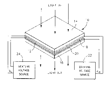
Referring to Figure 1 (which is exaggerated in scale), an
optical device 10 includes a layer of electro-opt~c material 12
sandwiched between a pair of transparent insulator plates 14 and 16
which may, for example, be glass or plactic~ Transparent electrodes
18 and 20, which may be indium-tin-oxide coatings, cover the inner
surfaces of the plates 14 and 16, respectively, on either side of the
electro-optic layer 12. Preferably, the electro-optical material 12
is a thin polymer film containing dispersed liquid crystal droplets
~so-called PDLC material). Examples of PDLC material are deseribed in
U.S. Patent No. 4,728,547.
A source 22 of driving voltage Vd is connected across the
electrode~ 18 and 20 for selectively applying a relatively low
frequency driving electric field to tb~ PDLC film 12. When the
driving electric field is not applied, the PDLC material 12 i9 in a
relatively opaque "light sca~tering" gtate in which ~he liquid crystal
droplets are randomly alignedO When the driving electric field is
applied, the PDLC material 12 switches to a relatively transparent
: 20 "non-light ~catterin" state in which the liquid crystal droplets are
aligned parallel ~o the electric field direction. The alternation of
the driving electric field avoids undesirable bias effects that would
, .
1 3 1 537~
otherwise be produced within the liquid crystal droplets if the
driving electric field ~AS unidirectional.
The PDLC electro-optic device lO may be useful in a number of
automotive applications requirin~ variable light transmission, e.g., a
flat-panel d.isplay, a privacy control window, or a solar control
sunroof. In such automotive applicatlons, however, it is importa~t
that the optlcal dPvice 10 be operable down to a relatively lo~
temperature (e.g., -20~C or even lower). This can present problems in
that, at such low temperatures, there may be a pronounced decrease in
the light transmissivity of the PDLC material 12 in the activated-
transparent state and/or the time required to s~itch the PDLC material
12 from the inactive-opsque state to activated-trAnspaxent state (and
vice versa) may be excessively long. The present invention provides B
remedy for these problems.
According to the invention, the PDLC electro-optic device 10
is subj~cted to dielectric hea~ing to raise its temperature and
thereb~ increase ies light transmissivity in the activated~transparent
state and/or decrease it~ switching time from the inactive-opaque
~tate to the activated-transparent stste (and vice versa~.
Specifically, a source 24 of heating voltage Vh is connected across
the electrodes 18 and 20 for ~electi~ely applying a r~latively high
frequency heating electric field to the PDLC layer 12. Both the
poly-er matrix snd the liquid cryetal droplets of the PDLC film 12 are
1 3 1 537~
dlelectric. Consequently, application of the heating electric field
produces dlelectric heatin8 of the PDLC material 12.
The amount of heat generated ~ithin thP elec~ro-optic de~ice
10 i8 dependent upon the density of polarizable electric dipoles
uithin the PDLC layer 12 and the frequency of the heating electric
fleld. In general, the higher the electric dipole density, the
greater the amount of dielectric heating. For most dielectric
materials, includi~g the PDLC material 12, maximum dielectric heating
occurs at a frequency in the MH~ range (~hich is somewhat
inconveniently high). Fortunately, a high density of electric dipoles
is present in both the polymer matrix and the liquid crystal droplets
of the PDLC materi-l 12. As a result, satls~actory dielectric heating
for purposes of the invention can be achieved at electric field
frequencies in the K~z range. Ho~ever, there may be a lower frequenc~
limit as described belo~. ~
~here the spplication of the electro-optic device I0 requires
that the heating and driving o the PDLC layer 12 be independent of
one another~ it i8 necessary that the frequency of the h-atin8
electric field be suffici~ntly higher than the frequency of the
driving electric field that the heating electric field does no~ cause
electro-optic s~i~ching of ~he PDLC film 12. This can be better
~ppreciated by co~sidering the frequency response of the PDLC material
12 ~hich is divisible into adjacent low and high frequency d~ains.
An applied electric field having a frequency within the lower
1 3 1 537~
~requency region al~gns the liquld crystal parallel to the field
direction (this is the sctivated-transparent state). An applied
clectric field having a frequency within the highsr requency region
aligns the liquid crystal perpendicular to the field direction (an
activated-opsque state). The boundary between the low and high
frequency regions is the so-called ~cross-over~ frequenc7. At
frequencies at or near the cross-over frequency, there is a kind of
deadband where the applied electric field has little or no
electro-optic effect on the liquid crystal.
From the foregoing, it ~ill be apparent that the driving
electric field should have a fr~quency that is ~ell belo~ the
cross-over frequency of the PDLC material 12. It is equally spparent
that the heating electric field should have a frequ ncy that iæ near
or a~ove the cross-over ~requency of the PDLC material 12. Typical
PDLC cross-over frequency values are iD. the several K~z range. This
means that the frequency of the heating electric field should be in or
above the several K~z range ~hile the frequency of the driving
electric field should be no higher than a few KHz at mo~t.
For 3implicity of illustration ln Figure 1, the driving
voltage source 22 and the hea~in8 voltage source 24 are shown as
independent voltage sources each connected to th~ same set of trans-
parent electrodes 18 and 20. ~here the driving and heating ~oltages
are simul~aneously applied to the electrodes 18 and 20, some
undesirable effects may ensue due to cross-coupling betw~en the two
1 3 1 537~
voltage sources 22 and 24. One way to avoid these unwanted cross-
coupling effects is by time division multiplexing the application of
the driving and heating electric fields. A second solution is to
combine the driving and heating voltage sources 22 and 24 as shown in
Figure 2.
Referring to Figure 2, ~ first voltage source ?6 provides a
first ~oltagP Vl of controllable frequency fl and a second voltage
source ~8 provides ~ second voltage V2 of controllale frequency E2.
The first and second voltages Vl and V2 are mixed together by a
frequency multiplier 30 and amplified by a voltage amplifier 32 ~o
provide a co~posite voltage Vc which is applied across the electrodes
18 and 20 of the electro-optic device 10. Due to the miYing action of
the multiplier 30, the composite voltage Vc is composed of ~ sum
frequency component f3 - (fl ~ ~2) and a~ difference frequency
lS component fd ~ (f~. ~ f2)-
When it is desired to simultaneously drive and heat the PDLCmaterial 12, the first and second voltage frequencies fl and f2 are
selected to produce a sum frequency f8 that is sufficienely high to
heat the mat~rlal 12 and R difference $requency fd that is
sufficiently lo~ to electro-opt~cally s~itch the material 12 (e.g., fl
50R~z, f2 ~ 49K~z, fg - 99RHz, fd ~ l~Hz). If it is desired to heat
the PDLC material 12 only~ the first and second voltage frequencies f
and f2 are selected to produce 5um and difference frequencies fs a~d
fd that are both suiciently high to heat the materisl 12 without
1 3 1 537S
electro-optically switching it (e.g., fl - lOOK~z, f2 - O.lRH~, fs
lOO.lKH~, fd - 99.9KHz). Conversely, if lt is desired to drive the
PDLC material 12 only, the firs~ &nd second voltage frequencies fl and
f2 are selected to produce sum and difference frequencles fs and fd
that are both sufficiently low to electro-optically s~itch ~he
material 12 withGut appreciably heating it ~e.g., fl ~ 0.5X~z, f2
0.4KHz, fs = O.9KHz, fd a O~lRHz) ~
In an arran~ement constructed and satisfactorily operated in
accordance with Figure 2, the follo~ing components ~ere employed:
Component Numeral
~ewlett-Packard Model No. 3325A ................. 26
Uavetek Nodel No. 187 . . . . . . . . . . . . . 28
Princeton Research Associatsd Mod~l No. 189 . . 30
Krohn-Hite Model No. 7500 . . . . . . . . . . . 32
Referring to Figure 1, another approach to eliminating un-
desirable cross-coupling betw~en the driving and heating voltage
sources 22 and 24 contemplates modi~ications to the electrodes 18 and
: ~ :
20. A~ least t~o al~ernative electrode conflgura~ions are available.
First, two ~eparate sets of electro~es lR and 20 may be prov~ded, a
different set for each of the drivlng and heating voltage sources 22
and 24, respectively. A second configuration involves dividing one of
~he electrodes 18 and 20 into two interdigltated electrodes as shonn
in Figure 3.
131~;~7'3
Referring to Figure 3, the electrode 18 is formed by two inter-
digitated electrodes 18a and 18b located on the same side of the PDLC
layer 12 for ease of manufacture. In one possible method of fabrica-
tion, the interdigita~ed elec~rodes 18a and 18b may be formed via a
deposition-masking-etching process. The driving voltage source 22 is
connected to apply the driving voltage Vd between the electrode 20 and
each of the electrodes 18a and 18b, respectively. The heating voltage
source 24 is conn~cted to apply the heating voltage Vh bet~een the
electrodes 18a and 18b such that the heating electric field appears as
a fringing electric field established between adjacent interdigitated
fingers of the electrodes 18a and 18b. A lou pass filter 26 is
inserted bet~sen the drlving voltage source ~2 and the electrode 18b
to electricall~ isolate the interdigita~.ed electrodes 18a and 18b at
the high frequency of the he~ting voltap,e Vh, i.e., the low pass fil-
ter 26 acts as a closed swi~ch to the low frequency driving voltage Vdand Acts as an open F~itch to the high ~requen y heating voltage Vh.
It ~ill be appreciated that the foregoing embodi~ents sre in-
tended to illustrate the invention without undue limitation,
recognizinR that various alterations and modlfications may be made to
these embodiments ~ithout departing from the spirit and scope of the
invention. ~s an example, the invention is not necessarily r~stricted
to optical devices emploging PDLG material, but ma~ rather embraca any
optical device to which the principles of the invention are
applicable.