Note: Descriptions are shown in the official language in which they were submitted.
~ 3 ~
CMOS Integrated Circuit Having Improved Isolation
Tech_al Field
This invention relates to semiconductor integrated circuits having both
n-channel and p-channel devices.
5 _ckground of the Invesltion
A comrnonly used device configuration in silicon integrated circuit
technology is referred to as CMOS, which is an acronym for Complementary
Metal Oxide Semiconductor. This configuration obtainecl its name because it usesboth p-channel and n-channel insulated gate field effect transistors. For best
10 opera~ion, the n-channel and p-channel devices shollld be electrically isolated from
each other, and are therefore frequently formed in "tubs", which a~e doped regions
in a silicon subs~ate. One method of forming the tubs is shown in U. S. patent
4,554,726, co-assigned herewith. In that technique, a pho~oresist is patterned to
expose portions of the substrate for the n-type tubs. Phosphorus and arsenic are15 implanted, followed by-photoresist stripping and oxidation of the n-type tub
surface. Boron is then implanted for the p-type tub, and the oxide stripped. A
dopant drive-in heating step is then accomplished to drive the dopants deeper into
the semiconductor substrate, thereby forming tlle n-type and p-type tubs.
A second boron impiànt into the p tubs is performed; subsequent
20 lithography then defines an opening in a masking layer at the boundary between
the n and p tubs. An oxidation s~ep follows, to form the "field oxide" regions,
which isolate the n tubs from the p tubs aî the surface of the substrate. The
second boron implant then forms the "channel stop" region under the field oxide
in the p tub, which aids in isolating the n-channel devices to be forrned ~herein.
25 In order to retain the second boron implant near the oxide/silicon interface, the
field oxide is formed during a relatively brief oxidation process that is
accomplished in steam at high pressure. Further fabrication steps to form the p-channel and n-channel field effect transistors (in the n tubs and p tubs,
respectively) follow the tub forrnation, according to techniques well known to
30 those skilled in the art.
While adequate for many prior art applications, the process described
above could be improved in several respects, especially as device geometries
shrink below 1 micron. For example, an improved channel stop for the n-channel
devices formed in the p tub would be desirable. Also, greater punch-through
35 resistance for the n-channel device would also be desirable.
~'3~5~
Summary of til~ ~nvel~tion
We have found that improved characteristics with a CMOS structure can be
obtained by using a chann~l stop implant of boron at a depth at least as great as the
depth of the field oxide in the silicon substrate. That is, the p-type channel stop implant
5 has an energy selected so that the peak concentration is just below the subsequently
formed field oxide. We have found that both the electrical isolation of the n-channel
devices, and the punch-through characteristics, may be simultaneously improved by this
technique, facilitating the use of the CMOS process in sub-micron geometries.
In accordance with one aspect of the invention there is provided a CMOS
10 integrated circuit having p-channel field effect transistors formed in a n-type region, and
n-channel ~leld effect transistors formed in a p-type region, wherein a field oxidc isolation
region overlies a portion of said p-~pe region adjacent to a source-drain region of a n-
channel field effect transistor, and wherein a gate electrode overlies a channel region
located between source-drain of said transistor, characterized in that said p-type region oE
15 said integrated circuit comprises a p-type impurity threshold adjust implant region
extending across said channel region, and still further comprises a p-type impurity channel
stop implant region extending under said channel region and said field oxide isolation
region throughout said portion of said p-type region that is overlaid by said field oxide
isolation region whereby the concentration of said p-type impurity threshold adjust implant
20 region is at a first maxima at the surface of said p-type region and the concentration of
said p-type impurity channel stop implant region is at a second maxima immediately below
said field oxide isolation region overlying said p-type region.
Brief Description of the Drawin~s
FIGs. I-5 are sectional views of a portion of a device fabricated according to
2 5 this invention.
FIG. 6 plots the boron concentration versus the depth in the substrate
underneath the gate oxide.
FIG. 7 plots the boron concentration versus the depth in the substrate
undemeath the field oxide.
For reasons of clarity, the elements of the devices depicted are not
drawn to scale.
Detailed Descript;l)n
The present invention concerns an improved method of forming
5 integrated circuits having both p channel and n channel devices. Referring to FIG. 1,
a CMOS integrated circuit is shown in an early stage of fabrica~ion. Depicted are
substrate 1, oxide layer 3 and photoresist layer 5. The photoresist ancl oxi~le layers
were patterned to expose selected portions of the substrate for the ion implan~ations
for the n-type tub. Both a phosphorus implant 7 and an arsenic implant 9 have been
10 made, as indicated by the open triangles and x's, respectively. As will be readily
apparent to those skilled in the art, these steps can he readily performed by a skilled
artisan without further description. The photoresist and oxide are stripped and an
oxidation step for the n-type tub is performed. The oxide is shown as region 11, and
the n-type region as 13. ~eE~rring to FIG. 2, a first boron implan~ for the l~-~ub is
15 performed, shown by dots 20. This implanl may be eilher shallow or deep. A tub
drive-in step is then perlormed, producing the n tub 15 and the p tub 17, as shown in
FIG. 3. The tub drive-in is followed by a second boron implan~ation, shown as open
squares 30. This second boron implant is the "deep" p-type implant according to the
present invention. This places the peak boron concentration as implanted at a depth
20 in the substrate sligh~ly grealer than the depth of the subsequently-formed field oxide.
- 2a -
~ 3 ~ 9
Consequently, the amount of boron segregation to the field oxide during the
subsequent steam oxidation is also reduced. The result is imyroved isolation forthe n-channel devices subsequently formed in the p tub. At this point, the n-type
lub oxide l I is stripped. Active region patterning and high pressure field
S oxidation are perforrned. The resulting structure is shown in FIG. 4, with a thin
oxide shown as region l9 and the field oxide shown as region 21.
In accordance with the present invention, the above-noted second,
"deep" boron implant has an energy selected so that the peak of the boron profile
will be located irnmediately underneath the field oxide, after the subsequent
lO oxidation step. This energy also creates a retrograde p-tub boron profile in the
channel region. That is, the peak concentration is below the substrate surface in
the chamlel region. The peak shoold be close lO the junction depth to improve
punch through resistance. It will also be appreciated by those skilled in the alt
that the use of high pressure steam oxidation to grow the field oxide reduces the
lS thermal cycle, and therefore creates less boron segregation into the field oxide.
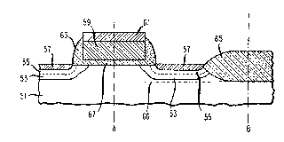
These features will be better understood by referring to FIG. S which
shows the structure after device fabrication, as well as the adjoining field oxide
region. Depicted are substrate Sl, lightly doped source/drain regions 53, heavily
;- doped source/drain regions SS, an~source/drain silicide contact regions 57. In
20 a~ldition, there is shown polysilicon gate region S9 and gate silicide contact region
61, silicon dioxide gate sidewalls 63, and field oxide 65. As shown, there is a
gate oxide 67 under the polysilicon gate S9, with the channel region being located
immediately under the gate oxide in the substrate. The approximate depth of the
peak concentration of the second boron implant noted above is ;ndicated by
25 dashed line 66. As can be seen, the peak lies just under the field oxide region 65
for improved channel stop isolation. In addition, in the device channel region, the
peak of the boron implant helps prevent punch-through between the heavily doped
source/drain regions S~.
The boron concen~ration profiles along lines (A) and (B) of FIG. S,
30 which are through the gate structure and the field oxide, respectively, are shown in
FM. 6 and 7, respectively, with the boron concentration plotted vertically and the
depth horizontally. The units for both are arbitrary units. As can be seen in FIG.
6, the boron concentration in the channel region (i.e., directly under the gate
oxidej has an initial high value at the surface. 1`his is accomplished by an
35 optional third boron implant, which is referred ~o as a "threshold adjustrnent"
implant in the art, and is a known technique used to raise the threshold voltage of
the n-channel device. However, this adjustment is not necessary in all devices,
- 3 -
~ 3 ~ 9
and may alternately be accomplished by other means, sllch as a p-doped
polysilicon gate. In the illustrative embodiment, the threshold adjustment implant
is accomplished using BF2 at a beam energy of 50 KeV, at a dose of
1.7xl0l2/cm2. The boron concentration then decreases from this high value at the5 surface to a minima at dl, and then increases to the peak at d2 before again
decreasing. The peak at d2 is due to the "deep" second boron implant noted
above, and the increase between dl and d2 is the "retrograde" profile refelTed to
herein. Refer~ing to FIG. 7, the boron concentration in the field oxide region has
a maximum at the oxide-substrate interface and continually decreases with depth
10 into the substrate.
The depth to which the l'deepll boron implant should be accomplished
therefore depends on the desired field oxide thickness. In order to determine the
implant depth, allowance is made for the greater thickness of silicon dioxide ascompared to the silicon consumed in its formation. That is, a given thickness of15 grown SiO2 consumes about 40 percent as much thickness of the silicon substrate.
For example, a field oxide region 65 having a thickness of 630 nanometers (6300
angstroms) consumes about 250 nanometers (2500 angstroms) of the silicon
substrate. Such a thickness may be grown at a pressure of 25 atmospheres in
steam, at a temperature of 900 de~rees centigrade for 25 minutes. Therefore, the20 boron energy is selected to implant to a depth of slightly greater than 250
nanometers. This may be accomplished using a b.eam energy of 125 IceV when
using bors)n ions. This energy is sufficient to place the peak concentration of the
boron at a depth of approximately 300 nanometers (3000 Angstroms) in the
substrate. A typical boron dose for this implant is 2.5xlOI2/cm2. Other energies25 and dosages will be easily selected by those skilled in the art as device design
varies and continues to evolve. We estimate that the field oxide thickness as
grown will be greater than 450 nanometers (4500 angstroms), thereby consuming
at least 180 nanometers (1800 angstroms3 of silicon. E~ence, the implant depth
according to the present technique will typically be at least 200 nanometers, and
30 more ypically at least 250 nanometers. However, a reduction in power supply
voltage below the current 5 volt standard (e.g., down to perhaps 3 volts) may
allow for thinner field oxide regions. Note that the depth referred to is from the
silicon surface as irnplanted, prior to field oxide growth, and remains substantially
this same value underneath the gate oxide of the n-chalmel devices. However, the35 field oxide is typically subjected to an etch-back procedure to reduce the "birds-
beak" effect, so that the field oxide thickness on the final device is typically only
about two- thirds of the thicknesses as grown.
- 4-
-
~ 3 ~ L 9
Note that the foregoing illustrative embodiment has been given for a
twin-tub CMOS process, wherein additional p and n dopants are used to define thetwo tub regions in a relatively lightly doped substrate (either n-type or p-type).
However, the present invention may also be uscd with a single p-type tub forrned5 in an n-type substrate. That technique is often referred to as a "single well" or
"single tub" process, and the n-doped substrate then forrns the region in which the
p-channel devices are formed. Still other variations are possible.
. ~ . \, ~