Note: Descriptions are shown in the official language in which they were submitted.
l 31~27
-
PHN 12.154 1 2.1.1988
Display device and method of driving such a device.
The invention re}ates to a display devioe
comprising an electro~optical displa~ medium between two
supporting plates, a system of pixels arranged in rows
and columns, with each pixel being formed by picture
electrodes arranged on the facing surfaces of the
supporting plates, and a system of row and column
electrodes for presenting selection and data signals by
means of which a range of voltages dependent on the
electro-optical display medium can be presented across the
pixels for the purpose of picture display.
The invention also relates to a method of
driving such a displa~ device.
A display device of this type is suitable for
displaying alphanumerical informatinn and video information
by means of passive electro-optical display media such as
liquid crystals~ electrophoretic suspensions and
electrochromic materials.
A display device of the type described in the
opening paragraph is known from the Netherlands Patent
Application no. 8502663 laid open to public inspeotion~
in the name of the Applica~. In the device shown in this
Application diodes are used as non-linear switching
elements in an active matrix, namely two diodes per pixel.
Two successive rows of pixels each time have one row
electrode in common. The drive mode is such that in
~ 25 tele~ision applications (for example with a drive mode
; ~ in accordance with the PAL or NTSC s~stem) the information
of two successive evan and odd lines is presented across
each pixel at an alternatine polarity and at the ~ield
frequency. The information of a pixel is therefore
determined by the average signal of two successive even and
odd lines. Since each time two rows of picture electrodes
are simultaneously written because two suocessive rows
e-oh time have one rov eleotrode in co:~on, suoh
31~27
P~ 12,154 2 2,1.1988
devica provides little flexibility as regards the choice
of co]our filters to be used. In fact, this choic~ is
limitedto strip-shaped colour filters.
It is an object of the invention to provide
a picture display device of the type described in the
opening paragraph in which the r~ electrodes are not
common and in which the rows of pixels are separately
driven without the omission of common row electrodes
leading to an increase of the number of connections.
~ 10 It is also an object of the invention to provide
-~ such a display de~ce ensuring a considerable freedom in
the choice of the colour filters to be used.
The invention is ~ased on the recognition that
it is possible to give the pixels a given adjustment per
row by char~ ng or discharging the capacitances
associated with these pixels after first having discharged
or charged them too far (either or not accurately).
To this end a picture display device according
; to the invention is characterized in that the device
comprises means to apply, prior to selection, an
auxiliary voltage across the pixels beyond or on the limit
of the voltage range to be used for~picture display.
The auxiliary voltage is preferably beyond or
on the limit of the range of transition in the transmis-
sion/voltage characteristic of the 0lectro-optical mediumO
A first preferred embodiment of a display
device according to the invention is characterized in
that the picture electrode on one of the supporting plates
is connected in an electrically conducting manner to the
33 common point of two non-linear switching elements which
are arranged in series between a column electrode for
data signals and an electrode for the auxiliary voltage.
The auxiliary voltage may then be a fixed
reference voltage so that all pixels in a row are first
charged negatively or positively to a fixed value and are
subsequently charged or discharged to the corrsct signal
value, dependent on the data signals presented.
.
131~427
- 3 - 20104-8451
Since this is effected for each individual row
without a subsequent row or previous row being influenced, the
picture information can be adapted to a colour filter to be used,
which colour filter may be composed of, for example, triplets
as described, for example, in the Canadian Patent Application
No. 520,565 filed on October 15/86 in the name of the Applicant,
or it may have, for example a diagonal structure.
Discharging and charging prior to the actual driving
operation with the picture informa-tion can be effected during
the same line period in which the picture information is
presented, but also during the preceding line period.
Since each row of pixels is now separately written,
the voltage across these pixels can also be inverted per row,
which leads to a higher face flicker frequency and hence to a
steadier plcture.
A second preferred embodiment of a device according
to the invention is oharacterized in that a Zener diode is
arranged between a pixel and a row or column electrode. In this
case the electrode for the reference voltage may be entirely
dispensed with, which leads to a relatively larger portion of the
surface of the pixel to be used for the actual display. In
addition the number of components in such a device is smaller,
which increases the yield. Finally the parasitic capacitance
is sma~ller whilst an optimum choice of possible electro-optical
materials and the Zener diode to be used is possible.
,~,
,:., '~
~ 3 ~ 7
- 3a - 20104-8451
A method according to the invention is characterized
in that prior to presenting a data signal the pixels are
charged positively or negatively to an auxiliary voltage beyond
or on the limit of the range to be used fo:r picture display.
The invention will now be described in greater detail
by way of example with reference to the accompanying drawings
in which
Figure l is a diagrammatic cross-section of a
` ` 13~ ~27
PHN 12,154 4 2.1,1988
display de~ice according to the invention, taken on
the line I-I in Fig. 2;
Fig. 2 is a diagrammatic plan view of the
device of Fig. 1;
Fig, 3 shows the associated transmission voltage
characteristic;
Eg, 4 is a diagrammatic representation of the
device;
Fig, 5 shows some drive signals associated with
the device;
Fig, 6 shows a modification of the previous
devi c e,
Figs. 7 and 8 show diagrammatically methods in
which a device according to the invention is used for
television display;
Fig. 9 shows an embodiment of a device according
to the invention comprising Zener diodes and
Fig. 10 shows the current-voltage characteristics
associated with the Zener diodes~ whilst
Fig, 11 shows a number o~ modirications of the
device of Fig, 9.
The Figures are diagramm~tic and not to scale.
Corresponding components are usually denoted by the same
reference numerals.
~: :
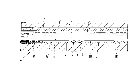
Figs. 1 and 2 show a diagrammatic cross-section
and a plan view of a part of a display device, in this
embodiment a liquid crystal display devicel which
has two supporting plates 2 and 3 between which, for example
a twis*ed nematic or a ferro-electric liquid crystalline
30 material 4 is prese~t. The inner surfaces of the -
supporting plates 2 and 3 have electrically and chemically
; insulating layers 5. A plurality of row and column-
arranged picture eIectrodes 6 of indi~m tin o~ide or anoth~
electrically conducting trans~arent material is provided
on the supporting plate 2. Likewise, transparent picture
electrodes 7 of, for example, indium tin oxide which are
integrated to strip-shaped row eleotrodes 11 are provided
~ 3 1 ~ 7
-
P~ 12.154 5 2.1.19~8
on the supporting plate 3. The facing picture electrodes
6, 7 constitute the pixels of the display device.
Strip-shaped (for example, metal) column elec-
trodes 8 are arPanged between the columns of picture
electrodes 6. Each picture electrode 6 is connected to a
column electrode 8 by a diode 9 diagrammatically shown
in Fig.2. As is apparent from ~ig. 2, the associated
column electrodes 8a, 8b areprovided between two picture
electrodes 6a, 6b. Furthermore liquid crystal
orienting layers 10 are provided on the inner surfaces
of the supporting plates 2 and 3. As is known, another
orientation state of the liquid crystal molecules and
hence an optically different state can be obtained by
applyinga voltage across the liquid crystal la~er 4.
The display device may be realised as a transmissive or a
; reflective device and may be provided with one or two
polarisers.
According to the invention auxiliary electrodes
18 which two picture electrodes 6 have in common in this
embodiment and which are provided on the side of the
picture electrodes 6 different from that of the column
electrodes 8 are also present between the columns of
picture electrodes 6. The auxiliary electrodes 18 connect
the picture electrodes 6 to a reference voltage vi~
diodes 19 which diodes are diagrammatically shown in Fig.2.
~; This reference voltage is chosen to be such that,
~; dependent on the voltages used on the selection line 11
and the electro-optical material used~ the capacitance
associated with the pixel can always be discharged via
the diode 19 to a voltage value beyond or on the limit of
the range o~ transition in the transmission voltage
characteristic of the relevant electro-optical materia~
Fig. 3 shows adiagrammatically a transmission/
voltage characteristic of a display cell as it occurs
in the display device of Fig. 1, 2. ~elow a given threshold
voltage (Vl or ~th) the cell substantiall~ passes no
light, wheroas above a given saturation voltage (V2 or
~3~27
PHN 12.154 6 2.1.1983
V~at) the cell i9 substantially entirely transpar2nt.
The intermediate range constitutes the above-mentioned
range of transition and is inclicated in Fig. 3 b~
means of bra~e 17. In this respect it is to be noted that
the absolutc value of the voltage is p]otted on the
abscissa, because such cells are usual]y driven at an
alternating voltage.
Fig. 4 shows diagrammatically the display device
of ~'igs. 1, 2. Pixels 12 constituted by facing picture
tO electrodes 6, 7 are connected via the picture electrodes
7 to row electrodes 11 at one end which together with the
column electrodes 8 are arranged in the form of a matrix.
The pixels 12 are connected to column electrodes 8 via
diodes 9. They are also connected via diodes 19 to an auxi-
liary electrode 18 which each time is common to two diodes19, 19'.
For writing information a first selection/
voltage Vsl is presented on a selection line 11 during
a selection period ts whilst the information or data
voltages Vd are simultaneously presented on the column
electrodes 8; this leads to a positive voltage across a
pixel 12 which represents the information presented.
To prevent degradation of the liquid crystal and
to be able to increase the so-called face flicker frequency,
~5 information h~ving an alternating sign is preferably
presented across the pixel 12, In a device according to
the invention a negative voltage across the pixel 12
which represents the information presented is achieved by
presenting a second selection voltage Vs2 while
qimultaneously presenting inverted data voltages t-~d)
after having discharged the capacitance associated with
the pixel 12 too far (or after having negatively charged it
too far),
Fig. 5 shows how the drive signals are chosen for
a plurality of ro~s of pixels 12 in order to write them with
picture information which changes sign during each field
(for example in TV applications).
~3~27
PHN 12.154 7 3.1.1988
From the instant to (see Fig. 5a3 a
selection voltage Vsl is presented on a row electrode 11
during a select:ion period t (which in this exa~lple is
chosen to be equal to a line period for TV applications,
namely 64 /usec) whilst information voltages or data
voltages Vd are simultaneously presented on the column
electrodes 8. After the instant t1 the row of pixels
12 is no longer selected because the row electrode 11
receives a voltage Vnsl. This voltage is maintained
10 until just before the next selection of the row of
pixels 12. In this example this is effected by giving
; the selection line 11 a reset voltage just before
again selecting the first row of pixels 12, namely at
an instant t3 = tf- ts in which t~ represents a field
period. The reset voltage and a reference voltage
presented on the common point of the diodes 9, 19~
can then be chosen to be such that the pixels 12 are
charged negatively to such an extent that this voltage
lies beyond the range to be used for picture displav
(up to a value of ~ -Vsat). In a subsequent selection
period ( from t4), -they are then charged to the desired
value determined by data voltages Vd. To this end the
row electrodes receive the voltage Vs2 and after the
selection period (a~ter t5) has elapsed they receive
a non-selection voltage ~ns2- In this way the voltage
across the pixels is inverted during each field period.
Fig. 5b shows the same voltage variation as
Fig. 5a but is then shifted over a ~ield period plus a
selection period (in this case a line period3. This
provides the possibilitv o~ wri-ting two successive
rows of pixels with inverse data voltages with respect
to each ot~er. Fig. 5c is identical to Fig. 5a, but is
shifted over two selection periods.
For (television) pictures with half the
vertical resolution in which the lines of the even and
the o~f field are written over each other
it is achieved that
~3~427
P~ 12.154 8 2.1~1988
the picture information changes its sign and is
replenished once per field period. Although the line
flicker frequency is 25 Hz (30 Hz) in this cas0, a face
flicker frequency of 50 Hz (60 Hz) is.achieved between
suocessive rows due to the phase differlence of 180
introduced by changing the sign per row.
The selection voltages Vsl and Vs2 may of course
also be chosen to be shorter than one line p0riod (64/use~.
In this case the reset voltage may alternatively be
presented during a part of the line period in w~ich
selection takes place provided there is sufficient t:ime
left to c harge the pixels 12~ The voltage variation on
the electrodes 11 is then effected, for example in the way
as shown diagrammatically in Fig. 5a by means of the broken
lS line 14,
The device shown is very suitable for using a
drive method in which Vc = VSa2~ th is chosen for the
average voltage across a pixel (see Fig~ 3) so that
the absolute value of the voltage for the purpose of
picture display across the pixels 12 is substantially
limited to the range between Vth and Vsa~.
A satisfactory operation as regards grey scales is
obtained if, dependent on the data voltages Vd on the
column electrodes 8, the voltage values across the
pixels 12 are at most Vc ~VdmaX=vsat an
Vc-Vd ax=Vth. Elimination of Vc yields: ~ Vd ~ max =
~(vsat-Vth)~ that is to say ~~Vsat Vth) ~ Vdmax
~(VSat-Vth~
In order to charge a row of pixels 12, for
example, positively, the associated row electrode 11 is
given a selection voltage Vsl--von-~(vsat+vth)
VO~ is the forward voltage of the diode 9. The voltage
across the pixel 12 is therefore Vd-V n-Vsl; it ranges
between ~2(VSat-vth)~(vsat~vth) $h
~( sat Vth)+~(VSat+Vth)=VSat dependent on Vd.
In order to negativel~ charge the same row of
pixels 12 (in a subsequent fie].d or frame pcriod) at a
~3~27
P~ 12.154 9 3.1.1988
subsequent selection with inverted data v~tages, these
are first char~ed negatively too far by means of a reset
voltagc Vreset on the row electrode 11 via diodes 19
oonnected to a reference voltageO Subsequently the selected
row electrode receives a selection voltage
s2 on+~Vsat~Vth) (in the same line period or in a
subsequent period). The pixels 12 which are negatively
char.g~cl too far are. now charged via the diodes 9 to
Vd-VOn-VS2, that is to say to values between
~Vsat~Vth)~2(Vsat~Vth)=~Vsat and
sat th) ~( sat Vth)=-Vth so that information with
the opposite sign is presented across the pixels 12.
In the case of non-selection the requirement
must be satisfied that neither diodes 9 nor diodes 19 can
15 conduct, in other words for the voltage VA at the junction
point 13 it must hold that VA ~ Vd and VA Vref or
VAmin ~ VDmax (1) and VAmax ~ Vref (2)o For the lowest
non-selection voltage Vnsl it then holds that:
(1) VA in=Vnsl+Vth VDmax = ~(Vsat~Vth)'
or
nsl ~ ~(Vsat~vth)-v-th (3)
It follows from (2) that
Vnsl~Vsat ~ Vref
Vnsl ~ Vref ~ Vsat ( )
Combination of (3) and (4) yields
Vref-VSat ~ Vn5l ~ ~(VSat-Vth)-Vth
Vref~ 3/2(VSat-vth) (5)
For the highest non-selection voltage Vns2 it similarly
30 holds that:
VAmin Vns2 sat ~ ~( sat th)
Vns2 ~ ~(Vsat Vth)~V~at(37) and
ns2 th ~ Vref or Vns2 ~ Vref~Vth (4')
35 Combination of (3i) and (4') yields;
ref th ~ Vns2 ~ ~(Vsat~vth)~vsat or
Vre~ ~ 3/2(VSat-vth) (5)
~3~27
PF~ 12.154 10 2~1 o1988
m e reference voltage 3/2 (V~at-Yth) t~us suffices to
block the diodes 19, 197 after writing both data and in-
versed data b~ means of the method described aboveO I~
summary it holds for the voltages Vns, V~, Vref and VreSet
that:
Vsl=-vOn- ~ sat*Vth);
V 2=-~ +~(VSat~vth);
Vnsl ~( sat th) th;
Vns2 ~(Vsat Vth)~Vsat;
Vref=3/2 (Vsat Vth);
VreS=Von~5/2Vsàt~3/2Vth-
When reversing the sign of the diodes 9, 19as is diagrammatically shown in Fig. 4a, the same type of
drive mode may be usedO Similar relations~ be it with
reversed sign~ then apply to the dri~e signals.
Fig. 6 shows diagrammatically a modification of
the device of Fig, 4, Since per column of pixels both
a column electrode 8 and an auxiliary electrode 18 is
present, such a realisation is at the expense of surface
area which may otherwise be utilised for picture electrodes~
Otherwise the reference numerals have the same significance
as in the previous embodiment. The drive mode is also
identical.
As has been stated, the advantage of a device
and a method according to the invention is that each row
of pixels can be separately driven without extra on
connection lines being required and with a free choice as
regards the colour filters to be used.
It has been described hereinbefore how the
information can be alternately reversed in sign for lines
to be written under a simultaneous inversion of the
selection voltages. The voltage across the pixel is
inverted. Figs. 7 and 8 show examples thereof.
In these examples subsequent picture lines are
denoted from the top to the bottom by means of the numerals
1~2, 3... 575 (PAL system~for the sake of simplicity.
The odd field thus comprises the lines 1, 3, 5~ ..0 575.
~ ~3~5~27
PHN 12 154 11 2.1.1988
the even field comprises the lines 2, 4, 6, .. 574,
Fig. 7 shows a first example in which the
first row 21 of pixels is first written with information
of the f`irst picture line (~ of the odcl field. The
5 secc>nd row 22 is subsequently written with inverted
information of the third pi ~ture line (-(3))~ that is to
say the second picture :~e of the odd field, the third row
23 is written with information of -the fifth picture line
(~(5)~, that is to say the third picture line o~ the odd
lO field, the fourth row 24 is written with inverted informa-
tion of` the seventh picture line (-(7)) 9 etc. In this
way 288 rows of pixels are first written with information
of the odd field in the so-called ha~f resolution mode.
Subsequently the same rows 21, 22, 239 24 are written with
information of the even field which is now presented with
opposite sign across the row of pixels (denoted by broken
lines). This means that the first row 21 of pixels is
read with inverted information of the second picture line
(-(2)), that is to say the first picture line of the even
field, the second row 22 is written with information of
the fourth picture line (~(4))7 that is to say the
second picture line of the even field~ etc.
In this way all pixels, considered with respect
to timel receive the average information of two successive
picture lines with the information of each picture line
per picture period being also inverted. Ihus row 21 shows
the average of the first and second picture lines (1/2)
and row 22 shows the average of the third and fourth pic-
ture lines (3/4), row 23 shows the average of the fifth
and sixth picture lines (5/6)~ etc. (see Fig. 7).
The minimum face flicker f`requency is then 50 H~ (PAL)
or 60 Hz (NTSC).
P`ig. 8 shows how a device according to the
invention can be similarly driven in f`ull resolution mode.
In this case 575 rows of pixels are read~ whilst the
information of one picture line (for example the third
picture line) is presente d in an inverted way to the
131~27
PHN 12.15~ 12 2.1.1988
second row 2~ (-(3) 3 and is presented unchanged to the third
row 23 (+(3~) o~ the pixels whilst simultaneously adapting
selection voltages. The data voltage is presented inverted
during half a line period whilst row 22 is selected and row
5 23 is not selected, and the other half of' the line period it
is presented unchanged whilst row 22 is no longer selected
and row 23 is selected.
Similarly the information of the fifth picture
line is presented inverted to row 2li(-5) and unchanged
1D to row 25(~5), etc. The lines of the even field are also
presented to the rows 21, 22, 23, 24, 25 in an inverted
form and in an unchanged form. In this way the average value
of two picture lines is presented across 575 rows of
pixels each time with an alternating sign of the ~oltage
15 across the display element, more specifically the average
value o~ the ~irst and second picture lines across row 21
(1/2), of the second and third picture lines across row
22t2/3), etcO (see Fig. 8). The rows are again entirely
independent as regards selection so that any colour filter
20 pattern can be used and the flicker is small (the face flick-
er frequenc~ is again 50 ~z (60 Hz) due to this drive mode).
Fig. 9 shows diagrammatically a device according
to the invention in which the auxiliary voltage is obtained
by using the Zener characteristic of a Zener diode 15.
25 Pixels 12 arranged in a matrix are again present at cros-
sings of row electrode,s 11 and column electrodes 8 whilst
the pixels 12 are connected to the row electrodes 11 via
the Zener diodes 15.
Here again it holds for a drive around
30 Vc= ~(VSatfVth) that with data voltages Vd(-~(Vs~t Vth)
~ Vd ~ ~Vsat-Vth)) the voltage across the pixels 12
can be limited to the range between Vth and Vsat. The
assoc~ed selection voltages are again Vsl=-VOn-~(Vsat~V~h);
VS2=~VOn~ (Vsat~Vth) -
It also holds that in the case of non-selection
at the point 16 the voltage must be such that there is
no conductance through the Zener diode, neither in the
forward direction nor as a Zener conductance,
~3~ ~42~
P.HN 12.154 13 2,1~1988
In this case allowance must be made for the
statistical behaviour of the 7ener diodes used. This is
shown diagrammatically in Fig, 10 in which the so~d~ine
shows a nominal current/voltage characteristic and the
limitation of the spreading range is indicated by means of
a broken line and a dot-and-dash line. Vzmin is the
highest admissible voltage at which the current ~or all
possible characteristics is stil.l sufficientl~ low to
prevent discharge within a field period of a capacitor
10 associated with a pixel. Vzmax is the lowest voltage to
cause the current passed through the Zener diode to be
sufficiently large to negatively charge a pxel to at
least -Vsat within the reset period (for example 64/usec).
For the lowest non-selection voltage (Vnsl~ these
15 conditions then lead for a voltage V~ (junction 16~ to
VAmax ~ Vnsl and VAmin ~ Vnsl VZmin
in which Vzmin is the said maximum zener voltage of the
zener diode 15 (see Fig. 10).
With VAmin=-Vdmax_vsat and VAmax=~d Vth
this leads ~so-called negative selection) with Vdmax_
~(Ysat-vth) to
dmax th ~ nsl ~ Amin Zmin'
: 25 ~( sat th) Vsat+VZmin 2 Vnsl ~ ~(Vsat-vth)-vth (6)~
for example
V l=~(V t-Vth)-~th-
In the same manner these conditions for the
highest non-selection voltage Vns2 (positive selection)
30 for which it holds that
V =-V +V and V =V +V lead to
Amin dmax th Amax dmax sat
Vdmax+Vsat - Vns2 S Vdmax+ th~ Zmin or
~( sat Vth)~Vth~VZmin ~ Vns2 ~ 2 (Vsat'Vth)~Vsat (7)
For example
Vnsl ~ ( Vsat Vth ) ~Vsat
~31~7
P~ 12.154 14 2.1.198~8
Addition of the left-hand and right-hand
members of the equations (6) and (7) leads to
( sat Vth)~2Vzmin ~ 2(Vsat~Vth) or
Vzmin ~ 2~Vsat - Vth)
The possibility of using this device i5 th~re-
fore determined by the minimum Zener breakdown voltage and
the maximum width of the transition range in the
10 transmission/voltage charEcteristic (denoted by brace 17
in Fig. 3) of the relevant liquid crystalline liquid or
another alectro-op~cal medium.
The maxi~um Zener breakdown must at least be
provided in order to discharge the pixels to a voltage
15 beyond or on the verge of the transmission range. ~or
the reset voltage it therefore holds that
V =V ~1(V TV )~V The device of Fig 9
reset Zmax 2 sat th sat'
can thus be driven with the same pattern of selection
voltages as is shown in Fig. 5 in which it now holds that
VSl=-von-~(vsat+vth);
V92=-von+~(vsat+vth);
Vnsl ~(Vsat Vth) th;
Vns2 2(Vsat Vth)+VSat;
' Vres=VZmax~2(Vsat~Vth)+Vsat-
30 ~ The invention is of course not limited to the
embodiments shown, but several variations are possible
within the scope of the invention.
In the~device of Figs. 4 and 6 non linear
switching elements other than diodes are possible such as,
for example, bipoLar transistors with short-circuited base-
collector ~unctions or MOS transistors whose gate is short-
.`'
~ 3 ~ 7
- 15 - 2010~-8451
circuit with the drain zone. There a,re also various possibili-
ties for the diodes themselves. In addition to the diodes which
are conventionally used in the technology for display devices,
for exampler a pn diode, Schottky diode or pin diode formed in
monocrystalline, polycrystalline or amorphous silicon, CdSe or
another semiconductor material may be considered, whilst the
diodes may be formed both vertically and laterally.
The Zener diade in the device of Figure 9 may
alternatively be arranged the other way around or it may be
present between the column electrode 8 and the pixel 12 as is
diagrammatically shown in, Figure 11. For such configurations
similar expressions for the (nan)-selection voltages, data vol~
tages and reset voltage may be derived as for the device of
Figure 9, whilst the same voltage values of the drive signals
apply for the device of Figure llb and the inverted voltage
values apply for the circuits according to Figures lla and llc.
In addition the availability of a reset voltage renders the
above-described device and method particularly suitable for use
~ in a ferroelectric display medium as described in the non-
pre-published Canadian Patent Application No. 561,154 filed on
March 10/88 in the name of the Applicant.