Note: Descriptions are shown in the official language in which they were submitted.
~31~
The present inventlon relate~ to a method for
controlling semiconductor ~wi~ches performing a d.c.-a.c.
conversion and connected in parallel with rectifying
components of a rectifier bridge connected to an a.c.
mains voltage supply, and to a control unit for applying
the method.
In many applications it i8 necessary that a
rectifier bridge us~d as a d.c. source permits both input
and output of power. Such a necessity i present e.g. in
an inverter fed from a constant-voltage supply and
controlling an a.c. motor handling a load that is capable
o~ delivering power. A typical load with such a
capability is an elevator car. Bidirectional power flow
may be implemented using e.g. transistor or thyristor
inverters in a.c. motor drives.
At present, bidirectional d.c. sources are often
implemented u~ing thyristor bridges connected between an
a.c. supply and a d.c. circuit. The thyrl~tor bridges,
which may work either with or without circulating
currents, supply power imparted by the load back into the
a.c. network. The operation of a circulating-current-free
thyri~tor bridge d.c. source i8 based on the principle
that one of the two bridges is conducting, depending on
the direction of the power flow. The time required for
changing bridges is relatively long. A circulating-
current-free circuit can also be implemented by means of a
diode bridge and a thyristor bridge, u~ing an
autotransformer to prevent power circulation. In this
case, the thyristor bridge, which performs the inversion,
can be held in the conducting state all the time~
In a circulating-current thyristor bridge
circuit, both bridges can also be held continuously in the
conducting state. In this case, there is no need for
sup~rvising the direction of the energy flow. The
drawbacks of thyri~tor circuits are the complexity of the
thyristor control circuit~ and the relatively lony time
required for firing and turning off the thyri3tor~.
~L31~4~
At present, d.c. source~ are also lmplemented
using diode bridges between a three-phase a.c. network and
the d.c. circuit. The diode bridge rectifies the three-
phase voltage when the direction of the power flow iB from
the a.c. network to the d.c. circuit. To convert the d.c.
voltage back into a three-phase a.c. voltage when the
power flows from the d.c. circuit into the a.c. network,
transistors are connected in parallel with the diodes of
the diode bridge. The transistor control voltages are
produced by diodes from the 3-phase voltage so that each
transistor conducts during the times when the diode
connected in parallel with i~ conducts. 'rhe conduction
times of the transistors are shortened to reduce the
circulating power by connecting a Zener diode in series
with the controller of each transistor.
When the motor is braked, the voltage in the
d.c. circuit of the frequency converter rises and the
inverting tran~i~tors connected in the rectifier bridge
are turned on, so that a current can flow from the d.c.
circuit into the a.c. network. As the transistors are
driven directly from the three-phase network by means of
diodes, the duration of the control pulse is constant.
This method has the drawback that, slnce the firing angle
ls constant, a c~rculating current, flowing through a
capacitor in the d.c. circuit, is always set up .
Moreover, networks using different voltages require
different control circuits, because the firing angle is
controlled by Zener diodes. In addition, the firin~ angle
is changed by variations in the mains voltage.
It i~ accordingly an object of the present
inventlon to eliminate the above-described drawbacks of
the prior art.
According to the invention, there is provlded a
method of controlling inverting semiconductor switches
35 connected in parallel with rectifyin~ components of a
rectifier bridge connected to an a.c. ~upply network,
comprising the ~teps of forming a reference voltage
comprised of a first voltage proportional to a phase
3 ~31~
voltage having the highest absolute value and a second
voltage proportional to a recti~ied voltage from the
rectifier bridge and controlling each of the semiconductor
switches by comparing a voltage proportional to a phase
voltage to said reference voltage.
With this method, the firing angle is
automatically adjusted to the correct value. Also, the
firing angle is the minimum required, thus reducing network
disturbances.
In the preferred embodiment of the method
according to the present invention, the reference voltage
is produced by subtracting from the first voltage the
difference between the second voltage and the first voltage.
Alternatively, the reference voltage can be
produced by subtracting the second voltage from double the
value of the first voltage.
Also according to the present invention there is
provided a control unit for controlling inverting
semiconductor switches connected in parallel with rectifying
components of a rectifier bridge connected to an a.c. supply
network, the control unit comprising comparator means for
comparing voltages proportional to the absolute value of
a phase voltage with a reference voltage for controlling the
semiconductor switches, and circuit means for generating
the reference voltages ~rom a first voltage proportional to
that phase voltage which ha~ the highest absolute value and
a second voltage proportional to a rectified voltage from
the rectifier bridge.
In the preferred embodiment of the control unit
according to the present invention, the circuit means for
producing the reference voltage comprising comparator
circuit means for generating the first voltage by selectiny
the highest of the phase voltages, differential circuit
means for producing the difference between the first voltage
and the second voltage and adder means for producing the sum
of the first voltage and difference obtained from the
differential circuit means.
13~8~
In this embodiment, the control unit comprises
diode means ~or preventing conduction by one of -the
semiconductor switches o~ each phase when the other is
conducting.
An embodiment of the present invention is
described below by way o~ example with reference to the
attached drawings, wherein~-
Figure 1 shows a squirrel cage motor, the power
stage of a frequency converter supplying the motor and a
unit controlling inverting transistors;
Figure 2 shows comparators, which compare a
voltage proportional to a highest phase voltage with a
reference voltage, and a circuit producing the reference
voltage;
Figure 3 shows a circuit for producing the
reference voltage in greater detail; and
Figure 4 is a more detailed view of the control
unit connected to phase R.
Figure 1 shows a squirrel cage motor M, which is
fed by a frequency converter. The figure also shows the
power stage of the frequency converter, in which the three
phases UR~ U5 and UT of the a.c. supply are recti~ied by
diodes D, - D,2 and the inversion is performed by transistors
Q, - Q6- zero diodes D, - D6 are also needed for the
inversion. Inductances L, - L3 and capacitors C, - C3
connected between the motor input conductors serve as noise
dampers. The rectified voltage, which is the di~ference
between the voltages ~V~ and -V~, is filtered by capacitor
CJ .
The energy generated when the motor is braking is
fed both into the resistor R1, controlled by transistor Q,3,
and into the three-phase network supplying the frequency
converter, by converting the d.c. into a.c. by means of
transistors Q, ~ Q.2, which are connected in parallel with
the diodes D7 - D,2 and controlled by the control unit 1.
Figure 2 shows the control unit, which turns on
each of the transistors Q, - Q,2 during a half-cycle o~ one
13~
of the phase voltages UR ~ U5 and UT when the absolute value
U, - U6 of the voltage proportional to the positive or
negative phase voltage exceeds the re~erence voltage VREf.
The voltages U~ - U6 correspond to the damped absolute values
of the positive or negative phase voltages +UR _UR ~ +U5 ~ ~
U5 ~ +UT or _UT The reference voltage VREF is produced by
subtracting, in the differential circuit 2, the dif~erence
between the voltage in the d.c. circuit, and the voltage VN~
which is proportional to that phase voltage which has the
highest absolute value, from this latter voltage VN~ said
difference being produced by another differential circuit
3, or by subtracting the voltage VD from the double value of
the voltage VN. The comparison is effected by means of
comparators 4-9, the output signals of which are used to
drive each of the transistors Q7 ~ Q.2 according to the power
needs. If the voltage in the d.c. circuit is equal to the
phase voltage with the highest ab~olute value, none of the
transistors Q7 ~ Ql2 conducts. If the d.c. voltage rises,
the reference voltage VREF falls and the transistors Q, ~ Ql2
conduct, and the more the d~co voltage rises, the longer the
transistors will remain conducting.
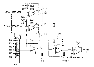
Figure 3 shows the circuit generating the
reference voltage VREF. A comparator circuit 10 produces the
voltage VN~ which is proportional to that phase voltage
2~ which has the highest absolute value. A selector switch
consisting of diodes Dl3 - Dla selects the one of the voltages
Ul - U6 which has the highest absolute value. The selected
voltage is input to the operational amplifier 11, which is
connected as a voltage follower with diode Dlg correcting the
diode threshold error caused by the selector switch. The
voltage VN appears at point A.
From point A, the voltage VN is passed to a
differential circuit 12, which produces the voltage VN ~ VD~
i.e. the difference between the said voltage VN and the
voltage VD~ the latter being proportional to the voltage in
the d.c. circuit. ~he voltage VN and a damped negative d.c.
voltage -V~ are applied to the input of the operational
1 3 ~
amplifier 13. The difference obtained and a damped positive
d.c. voltage +VDC are input to another operational amplifier
14. Diodes D20 - D23 protect the operational ampli~iers 13 and
14 against excessive absolute voltages.
The adder 15 adds the voltage V~ to the difference
VN ~ VD obtained from the differential circuit 12. A negative
reference voltage -VREF is obtained at the output of the
operational amplifier of the adder circuit 18. To obtain a
positive reference voltage +VREFI this negative voltage must
be input to an inverting amplifier 16.
Figure 4 shows the part of the transistor control
unit which drives transistors Q7 and Q~, connected to phase
R. The transistors connected to the other phases are driven
in a corresponding manner. The phase voltage ~R is damped
and applied to the input of an OP-amplifier 17, which outputs
a voltage U2, shown in Figure 3, which corresponds to the
negative half-cycle and is proportional to the phase voltage.
A voltage Ul corresponding to the positive half-cycle is
obtained by inputting the phase voltage to an inverting
amplifier 18. In the amplifier 17, capacitor Cs takes care of
noise filtering and diodes D24 - D2s protect the amplifier
against excessive absolute voltages.
The voltage U2 obtained from amplifier 17 is applied
to one input of each of the two comparators 19 and 20. The
other input of the first comparator 19 is connected to the
negative reference voltage _VREFI while the other input of the
second comparator 20 is connected to the positive reference
voltage +VREF- Transistor Q7 is controlled by the first
comparator 13 and transistor Qa by the second comparator 20.
To provide a drive signal for transistor Q7, the signal
obtained from the comparator 19 is passed via diode D26 into
an amplifier 21, where it is
B
11 3 ~
amplified, and appl~ed to the LED D30 of the optoisolator
of the tran~istor controller. Slmilarly, transistor Q8 i5
controlled by means of diode D27, amplifier 22 and LED
D31. The function of dlode D28 is to block the passage of
the -~ignal through diode D27 and thereby prevent
conduction by translstor Q8 when translstor Q~ i5
conducting. ~imilarly, diode D29 blocks the signal
passage through diode D26 and thus prevents conductlon by
transistor Q~ when transistor Q8 is conduc~lng.
It will be obvlous to those skilled in the art
that the em~odiments of the invention are not restricted
to the example described above, but that they may instead
be varied in the scope of the following claims.