Note: Descriptions are shown in the official language in which they were submitted.
~ 3 ~
C-31~
AULT CARTRIDGE
HAVING CAPACITIVE COUPLING
FIE~D OF THE INVENTION
The present invention relates to a data storage module,
or vault cartridge and, in particular, relates to a
vault cartridge having a capacitive coupling means for
coupling data and other signals into and out o the
cartridge.
BACKGROUND OF THE INVENTION
It has been known to use a data storage module, or
lS vault cartridge, in such applications as credit cards
and in controllers couplPd to a host system. A
particular problem associated with the use of such
modules is that in order to couple data into and out of
the module it is often a requirement that electrical
terminals be exposed upon a surface of the module.
These terminals m~ay take the form of a card edge
connector type terminal or other types of exposed
conductive surfaces which are operable for being mated
with a suitable connector in a receptacle to which the
module is coupled. The terminals may also take the
form of optical data transmis~ion and reception
devices. The exposure of the terminals may be
disadvantageous for several reasons. For example,
electrically conductive terminals may, under the
influence of atmospheric moisture and contaminants,
become oxidized thereby decreasing the conductivity of
the terminals. Another disadvantage is that the
~k
~3~8~
terminals are exposed to sources o~ electrical
discharge energy, such as static electriciky. As is
well Xnown, static electricity may cause the
degradation or the complete ~ailure o~ integrated
circuit devices which are subjected to a discharge of
static electricity. Such integrated circuit devices
may typically be included within the data storage
module for the storage of data and for performing
functions associated with the storage of the data.
Optical-type terminals may also be susceptible to
conducting static electrical discharges into the
storage module. Also, the radiation transmission and
reception means, such as a lens, must be maintained
free of radiation absorbing contaminates such as dirt
and grease.
Due to this requirement of previou~ data storage
modules that the data coupling terminals be in physical
contact or otherwise physically accessible to the host
system mating terminals, the exposure of the terminals
upon a surface of the data storage module can result in
the overall degradation of the operation of the module
or even in the complete failure of the module to
reliably store data. This problem is especially acute
in relatively small and portable data storage modules
which by definition may be inserted and removed a
nu~ber of times from a host system. Such modules may
also be especially vuln~rable in that they are
typically carried about in a jacket or shirt pocket
where the danger o~ exposure to static electric
discharge is increased.
It is therefore an objective of an aspect of the
invention to provide a vault cartridge which does not
have data signal coupling conductors exposed upon a
surface of the cartridge.
It is an objective of an aspect of the invention to
provide a vault cartridge which has data signal coupling
means enclosed within a nonconductive protective
covering of the cartridge~
It is an objective of an aspect of the invention to
provide a vault cartridge having conductive plate-like
members disposed beneath an insulating covering of the
cartridge, the plate-like members forming, in
conjunction with plate-like members in a vault in
receptacle, a plurality of capacitors for capacitively
coupling data and other signals into and out of the
cartridge.
SUMMARY OF THE INVENTION
Various aspects of the invention are as follows:
A system for storing data within a data storage device0 comprising:
means for storing data;
means for enclosing said data storing means, said
enclosing means having walls comprised of a material
which i9 substantially electrically nonconductive and5 which has a dielectric constant associated therewith;
a first plurality o~ conductive plate m~ans
disposed within said enclosing means and substantially
adjacent to an inner surface of at least one of said
walls;
iJ ~ J ~
a plurality o~ electronic data receiving means,
individual ones of which are coupled to individual ones
of said ~irst plurality of plate means, each of said
data receiving means having an output operatively
coupled to said data storing means;
a second plurality of conductive plate means being
disposed substantially adjacent to an outer surface of
at least one of said walls, individual ones of said
second plurality of plate means further being disposed
substantially in opposing relationship with individual
ones of said Pirst plurality of plate means such that
corresponding ones of said first and said second plate
means are operable for defining an electrical
capacitor; and
a plurality of electronic data transmission means,
individual ones of which are coupled to individual ones
of said second plate means for capacitively coupling
data for storage within said data storing means through
corresponding ones o~ said ~irst and second plate means.
A vault cartridge for storing accounting data in a
value printing system compxising:
an integrated circuit data storage device operable
for storing digital data expressive of accounting data
related to the printing of items having a monetary5 value;
an enclosure for enclosing said data storage device
within; and
a first plurality of conductive plate-shaped
members coplanarly disposed along at least one inner
surface of said enclosure, each of said first plurality
of members being operatively coupled to said data
storage device, each of said first plurality of mambers
further being disposed in opposing relationship with a
second plurality of plate-shaped members coplanarly
disposed along an outer sur~ace o~ said enclosure such
~ ~3~ $~
4a
that opposing pairs of plate~shaped members each define
a capacitor operable for coupling the accounting data
into said data storage module for storage within said
data storage device.
A method of storing data within and retrieving stored
data from a data storage device, the device b~ing
disposed within a protectiv~ module, comprising the
st~ps o~:
contacting a first plurality of electrically
conductive plate-shaped members upon at least one outer
surface of the module, individual ones of the first
plate-shaped members being operatively coupled to a
first data transmission and reception means;
providing a data storage device within the module;
providing a sscond plurality of electrically
conductive plate-shaped members upon an inner surface of
the module, individual ones of the second members ~eing
provided in opposing relationship with individual ones
of the first plurality of members, individual ones of
the second plurality of members further being
operatively coupled to a second data transmission and
reception means;
operatively coupling the second data transmission
and reception means to the data storage device for
providing data inputs and outputs and data storage and
retrieval control commands to and from the device; and
capaci~ively coupling data to ba stored from the
first data transmission and reception means through
opposed pairs of the first and second members and into
the storage device through the second data transmission
and reception means.
BRIEF DESGRIPTION OF THE DRAWINGS
The foregoing aspects and other features of the
invention will become more apparent in the following
4b
detailed description of the invention taken in
conjunction with the accompanying drawings wherein:
Fig. 1 is a block diagram showing a portable data
storage module, or vault cartridge, coupled to an
application host computer through a value receptacle;
Fig. 2 is a cutaway view~ in block diagram form, o~ a
vault cartridge coupled to an application host computer;
i \. .
~3~3~:~
Fig. 3 is a to~ view showing conduckive plate members
disposed beneath one surface of a vault cartridge;
Fig. 3a is an elevational view showing the vault
cartridge of Fig. 3 and a pair of opposed cartridge
engaging members;
Fig. 4 is a simplified schematic diagram showing
circuitry operable for unidirectional capacikively
coupled transmission and reception of digital signals;
and
Fi~. 5 is a simplified schematic diagram showing
circuitry operable for bidirectional capacitively
coupled transmission and reception of digital signals.
. .
DETAILED DESCRIPTION OF THE INVENTION
Referring now to Fig. 1 there is shown in block diagram
form a system having an application's host computer 1
bidirectionally coupled to a vault subsystem which
comprises a vault cartridge 2 coupled to a vault
receptacle 3. Application's host computer 1 is also
bidireationally coupled to a printer subsystem 4 and is
further bidirectionally coupled to an application's
environment 5. In general, host computer 1 may be any
data processing means operable for executing an
application program, such as a computer operable for
executing a postage dispensing application program.
The application's environment 5 may include a user of
the host computer or may also be another computing
system which is coupled to the application's host
computer and is operable for transmitting data to and
~ 3 ~ J~
receiving data from the application's host computer 1.
Th~ block designated as 5 may comprise a familiar CRT
screen and a keyboard which are both operable for
providing an operator with a means ~or interacting with
the application's host computer 1. Vault cartridge 2
may comprise a data storage means operable for storing
data generated by the application's host computer 1.
The vault cartridge Z may also comprise, for example,
ascending and descending postage registers which are
maintained within the cartridge 2 in a secure
environment. The vault receptacle 3 may be an
electromechanical mechanism haviny electronic and
electrical power coupling means for coupling data into
and out of the vault cartridge 2 and also ~or providing
lS operating power thereto. In accordance with the
invention, the vault cartridge 2 may be detachably
coupled to the vault receptacle enabling the cartridge
to be removed and inserted as desired by a user or some
operator of the system. Printer subsystem 4 may be any
suitabl~ printing means which is operable for receiving
data from the application's host computer ~or printingO
The printer subsystem 4 may be a printer operable for
printing a postage indicia which is representative of a
monetary value of postage. Printer subsystem 4 may be
a secure printer system which is bidirectionally
coupled to the application host computer 1 for
receiving there~rom and transmitting thereto security
codes such a~ cryptographic codes which enable the
printer subsystem 4 to print. Although shown as a
plurality of separate blocks, it should be realized
that the application's host computer 1, the vault
cartridge 2, the vault receptacle 3 and the printer
subsystem 4 may all be contained within a single
system. That i~, these blocks may not be independent
':
~ 3 1 ~
systems but the functions thereof may all be
incorporated within one system. Similarly, different
combinations of the blocks are possible such that the
application's host computer 1 and the vault receptacle
may comprise one system having a printer subsystem
coupled thereto through a suitable cable or some other
data transmission means.
As an example of the operation of such a system, the
application's host computer 1 may receive a request
from the application's environm~nt 5, such as a request
from a user to print a postage indicia representative
of a monetary value of postage. In response thereto,
the application's host computer 1 may interrogate the
vau~t cartridge 2 within vault receptacle 3 to
determine if the descending register securely contained
therein indicates a sufficient value of postage funds
to print the desired value of postage. Upon receiving
an indication from the vault cartridge 2 that such
funds are available the application's host computer may
thereafter send data to the printer subsystem 4 which
causes the printer subsystem 4 to print the postage
indicia indicating the desired monetary value~ Of
course, such a system as depicted in Fig. 1 may be
adapted to a wide number of applications such as the
printing of lottery tickets or the printing of tax
stamps, such as the stamps affixed to liquor and
cigarettes.
Referring now to Fig. 2 there is shown in block diagram
form a portable data storage module device, or vault
cartridge 10, coupled to an application's host
computer, or host device, 12. Vault lO is comprised of
a data storage means such as a random access memory
:
~L 3 ~
(RAM) 14 which is opera~le ~or the read/write storage
of data within. RAM 1~ may be a nonvolatile data
storage device. For example, RAM 14 may have a baktery
coupled thereto for maintaining the data stored
within the RAM 14 when the vault 10 is uncoupled ~rom
the host 12. Vault 10 may also comprise memory
interface 16 which i5 operable for providing address,
data and control lines to the RAM 14 for storing and
retrieving data therefrom. Interface 16 may also
comprise data transmission and reception circuitry. 0~
course, inter~ace 16 may also comprise a data
processing means such as a microcomputer device having
program and data storage and which is operable for at
least storing and retrieving data within RAM 14.
In accordance with the invention, vault 10 also
comprises a plurality of conductive members such as
plates 18a through 18f, the plates 18 being
conductively coupled to intsrface 16. As can be seen,
the plates 18 are disposed beneath an outer surface 20
of the vault 10. The surface 20 can be seen to be the
outer surface of a module casing or enclosure 21 which
may be comprised of an insulating thermoplastic
material. The enclosure 21 serves to both protect the
components within the vault 10 and also serves as a
capacitor dielectric material, as will be discussed
hereinafter.
Host 12 can be seen to comprise a vault receptacle 13
which may be physically separate ~rom the host 12 or
integrally joined thereto. Receptacle 13 comprises a
plurality of conductive members such as plates 22a
through 22f which are disposed such that these plates
22 are in registration with corresponding plates 18a
~ 3 ~
through 18f when vault 10 is fully inserted within the
receptacle 13. Plates 22 may be placed in physical
contact with the outer surface 20 of enclosure 21 by
the operation of the vault receptacle 13, the
receptacle being operated to insert, retain and
withdraw the vault 10. The vault 10 may be inserk~d in
the direction indicated by the arrow A. Plates 22 are
coupled to a host interface 2~ which in tuxn may be
coupled to a host data controlling device, such as a
central processing unit (CPU~ 26. Host interface 24
may comprise data transmission and reception circuitry.
It should be appreciated that host 12 may be the
applications's host computer 1 of Fig. 1.
As is apparent in Fig. 2, when the vault 10 is fully
inserted within the r~ceptacle 13 adjacently disposed
plates, such as the plates 18a and 22a, form the
opposing plates of an electrical capacitor. The
material of enclosure 21 between these plates sexves as
a capacitor dielectric material. In accordance with
the invention, each of these capacitors so formed, in
conjunction with interfaces 16 and 24, is operable for
the transmission and reception of data and other
signals therethrough.
Although six such capacitoxs are shown in Fig. 2, it
should be realized that more or les~ than six
capacitors may be employ~d for a given application. As
an example, eight such capacitors may be provided for
coupling a byte comprised of eight bits of data,
another eight capacitors may be provided for coupling
eight memory address lines and one or more capacitors
may be provided ~or coupling a memory control line such
as a read or a write control line or for coupling a
J
synchronization signal such as a constant frequency
clock signal. For example, with 17 such lines provided
it is possible for the host 12 to stsre and retrieve up
to 256 eight bit bytes of data ~rom the memo~y 14.
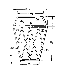
Referring now to Fig. 3 there is shown a top view of
one embodiment of a vault cartridge 30 having a
plurality of conductive plates 32 disposed beneath a
top surface thereo~. In Fig. 3 the top surface of the
cartridge 30 has been cut away to show the plates.
It can be seen in Fig. 3 that cartridge 30 may have a
planar asymmetrical shape which resembles two
trape20ids each having a common, equal base (B) and
unequal heights (Hl and H2) measured from the base.
Such a shape results in the cartridge 30 having
inwardly tapered side surfaces which may have an angle
of approximately 15 as measured from the common base.
When installed within a suitable receptacle the
cartridge top and bottom surfaces, as shown in Fig. 3a,
may be firmly engaged between an opposing pair o~
engaging members 36a and 36b, each of the engaging
members 36 having corresponding plates whereby the
individual signal and ground coupling capacitors are
formed. In operation, the insertion of cartridge 30
into receptacle 13 cause~ the movement of members 36a
and 36b as depicted by arrows B and C. When fully
inserted, cartridge 30 is securely interposed between
members 36, the top and bottom surface plates of
30 cartridge 30 being aligned with the corresponding
plates of members 36.
As can be seen, the plates 32 may have an essentially
triangular shape such that the utilization of the
~ 3~
surface area of cartridge 30 is optimized. In
accordance with the invention, each of the plates 32 is
coupled within the cartridge 30 to a suitable data
transmission and reception circuit. Also provid~d on
the surface of cartridge 30 may be an essentially
trapezoidal plate 34 which is operable for providing a
ground reference with a host system. Due to the
asymmetrical ~hape of cartridge 30, the cartridge may
be installed within a corresponding receptacle in only
one given manner, such as in the direction of the arrow
A, thereby facilitatin~ the alignment and registration
of each of the plates 32 and 34 with a corresponding
plate of similar shape within the receptacle. The
plate configuration as shown in Fig. 3, it should be
realized, may be duplicated upon a botto~ surface of
the cartridge 30. Thus, a total of 24 capacitive
plates may be provided ~or the coupling of digital
signals while two plates are provided for the coupling
of the ground reference. It should be further realized
that each of the plates 32 and 34 is preferably
disposed beneath the insulating surface (not shown) of
cartridge 30, the enclosure material serving as a
capacitive dielectric. The individual plates may be
fabricated by a number of well known methods, such as
by forming all of the plates 32 and 34 upon a surface
of a common nonconducting substrate 35 by well known
printed circuit fabrication techniques.
3 2 ~
12
In a preferred embodiment, the ~pproximate dimensions
~in inches) shown in Fig. 3 are as follows:
B = 3.5
Hl = 1.0
H2 = 3.5
W1 = 2.
W2 = 2.7~
b = 0O75
h = 1.5
bl = 3.75
hl = 0.9
Of course, the overall shape of device 30 of Fig. 3 and
the shape, dimensions, number and placement of the
plates 32 and 34 is illustrative only, it being
realized that the particular shape, dimensions, numbPr
and placement of the plates is a matter which may be
application dependent.
Referring now to Fig. 4 there is shown one embodiment
of interface cixcuitry which is operable for coupling a
signal through a pair of opposing plates, such as the
plates 18a and 22a of Fig. 2. As can be seen, the
plate 22a is coupled to the output of a driver device
40 within the host 12. The input to driver device 40
may be a data line or an address line the state of
which is typically controlled by CPU 26. The opposing
plates 18a and 22a form a capacitor having a dielectric
material interposed between the plates, the dielectric
comprisirg an interposed portion of the enclosure 21 of
the vault 10. As can be seen, each of the devices 40
and 42 may have a ground reference coupled therebetween
~ 3 3~ ~ ", .
13
by a capacitor formed by the plate 34 o~ Fig. 3 and a
corresponding plate 34a in the vault receptacle. A
diode 44 may be provided at the input to device 42 for
clamping the transmitted data signal to the ground
reference. Of course, the diode may be integrally
formed within the semiconductor device 42, it being
well known that such semiconductor devices often have
diodes, such as Schottky diodes, provided at their
inputs.
In operation, device 40 will provide an electrical
potential upon the plate 22a. This electrical
potential will be coupled through the dielectric
material of the enclosure 21 resulting in the transfer
of charge to plate 18a. This charge i5 detected by
device 42 and is expressed in the output of device 42.
Thus, it can be seen that if device 40 impresses a time
varying electrical potential upon plate 22a that the
output of device 42 will be expressive of the time
varying input signal to device 40. This capacitive
coupling technique of the invention is well suited for
coupling digital data at high speed through the
opposing plates 18a and 22a.
Referring to Fig. 5 there is shown circuitry operable
for the bidirectional communication of data through a
single pair of plates such as the plates 18a and 22a.
As can be seen, each of the plates is provided with an
opposing pair of data drivers and receivers in addition
to the driver 40 and receiver 42 of Fig. 4. These
additional drivers and receivers 46 and 48,
respectively, may each be provided with an active low
enabling input 50 and 52, respectively, while driver 40
and receiver 42 are each provided with an active high
1 3 ~ c~ ~J ~) _~.
1~
enabling input 54 and 56, respectivelyO Thus, it can
be seen that when an ENABLE signal is at a logic high
that the lower driver/receiver 40 and 42 is operable
for transmitting a bit of data from the right to the
left as shown in Fig. 5 while the upper pair 46 and 48
is disabled. When the ENABLE signal is at a logic low
level, the upper driver/receiver pair 46 and 48 is
operable for transmittin~ a bit of data from the left
to the right o~ Fig. 5, while the lower pair 40 and 42
is disabled~
of course, a number of different types of suitable data
drivers and receivers may be utilized for transmitting
and receiving bits of information through a respective
pair of capacitive plates, it being realized that the
devices shown in Figs. 4 and 5 are illustrati~e only.
It has been founh that if each conductive plate of a
pair of plates, such as the triangular plates 32 of
Fig. 3, have a surface area of approximately 0.7 inches
and that if the plates are separated by an enclosure
wall having a thickness of approximately 0.02 inch, the
enclosure wall material having an intrinsic dielectric
constant of approximately 4.0 to 4.9, that the
capacitance value associated with a pair of such plates
will be in a range of approximately 12 to 35 picofarads
at a frequency of approximately one MHz. This value of
capacitance is within the range of capacitance which
may be driven by an integrated circuit data
transmission device at a high data transmission rate.
As has been stated, the use of the invention may prove
advantageous in a number of different types of systems.
One such system is a value printing system such as a
~ ~ ,
$ ~ ~
system operable for the printing of postage, or a
system operable ~or printing tax stamps or tickets for
entertainment eventsO
In a postage printing system, for example, it is a
requirement that the value o~ postage printed or
otherwise dispensed be accurately accounted for. This
postage accounting data is typically maintained in
ascending and descending registers, the registers
typically being stored within a non-volatile data
storage devic~. In order to recharge the postage meter
with funds the descending register has stored within a
value expressive of the funds. This recharying is
typically accomplished at a postal facility by
physically removing the entire postage meter to the
facility.
As can be appreciated, the use of the invention permits
a data storage module, such as the vault cartridge 30
of Fig. 3, to be removed from the host system 12, which
host system may include a postage indicia printing
means. The cartridge 30 may thereafter b~ conveyed to
a recharging facility, perhaps by mailing the
cartridge, where the cartridge 30 is recharged with
postal funds. That is, data representing postal funds
is stored within the memory of the cartridge 30~ The
recharged cartridge may thereafter be inserted into th~
vault cartridge receptacle to resume the printing of
postage. Due to the capacitive data coupling apparatus
and method o~ the invention, the cartridge terminals
are not exposed at any time to possibly damaging
environmental factors, thereby assuring the sezurity
and integrity of the valuable postage accounting data
stored within.
,. ~ . - .
,
~ . `
.
16
It should be realized that illustrative embodiments
only of the present invsntion have been provided above
and that a number of modifications to the illustrative
embodiments may become apparent to those skilled in the
art. Therefore, the embodiment~ disclosed herein are
not meant ~o limit the invention, instead the invention
is meant to be limited only as defined by the appended
claims.
, . :