Note: Descriptions are shown in the official language in which they were submitted.
1 3 1 62 1 0
EXCITATION SUPPLY FOR GAS DISCHARGE TUBES
Field of the Invention
This invention applies to the field of excita-
tion of gas discharge tubes and more particularly to
switching power supplies used for exciting neon, argon,
etc., gas discharge tubes.
Background of the Invention
The most common gas discharge tube in use
today is the neon sign. ~hen a current is passed
through an inert gas such as neon or argon held in a
discharge tube, the gas will glow at a characteristic
color, such as red in the case of neon. In order to
excite the gas in a discharge tube, a sufficiently high
voltage must be maintained between electrodes on either
end of the discharge tube to allo~ current to flow.
This calls for a high voltage power supply to drive the
tube.
Excitation power supplies, and in particular
neon light transformers of the prior art, have been
known for many years. The most common neon light trans-
former is a 60Hz, 120VAC primary with a 60Hz approxima-
tely 10KV secondary which is directly connected to the
electrodes attached to either end of the neon sign. A
transformer of this size tends to weight 10-20 pounds
due to the massive core, number of primary and secondary
windings, and the potting of the transformer in a tar-
like material to prevent arcing. This results in a very
large, bulky and unsightly excitation supply.
More recently, light-weight switching power
supplies have been used to step up the 60Hz 120VAC
voltage to a higher frequency, higher fixed voltage
level for exciting discharge tubes. In general, the
1316~1~
--2--
switching frequency is fixed at the factory and not
matched against the load impedance of the gas discharge
tube to which it is attached, resulting in a fixed out-
put voltage. This impedance mismatch causes a great
loss in efficiency and sometimes an interesting side
effect. The length and volume of the discharge tube as
well as the gas pressure, temperature and type of gas
used in the discharge tube all have an effect on the
characteristic impedance of the discharge tube. A fixed
frequency, fixed output impedance excitation supply
attached to a variety of gas discharge tubes may cause
impedance mismatches which could result in the "bubble
effect". This effect is caused by standing waves
appearing at a high frequency within the discharge tube,
resulting in alternate areas of light and dark in the
tube. The standing wave may not be exactly matched to
the length of the tube, resulting in a scrolling or
crawling bubble effect in which the bubbles slowly move
toward one end of the tube. This may be an undesirable
effect in some neon signs, or may be desired in others.
The problem, however, is that with fixed frequency out-
put gas discharge tube excitation supplies, the
resulting effect is unpredictable.
The prior art also developed variable fre-
quency switching power supplies for exciting gas
discharge tubes to make the foregoing bubble effect more
predictable. By attaching an excitation supply to a gas
discharge tube and varying the frequency, one could
either eliminate or accentuate the bubble effect. This
resulted in an acceptable solution to the unpredic-
tability of the bubble effect, but did not solve the
impedance mismatch problem or allow a variable output
voltage for setting the optimal brightness. In order to
get the best transfer flow of power from the excitation
. ' ~.. : .
1 3 1 6 f t O
supply through the gas discharge tube, the output impe-
dance of the switching supply must be matched to the
input impedance seen at the terminals of the discharge
tube. The frequency at which this impedance match is
most closely satisfied may actually result in a bubble
effect when one is not needed, or may not result in a
bubble effect when one is desired. In order to satisfy
the user with the correct esthetic result the frequency
must be varied, which may result in an impedance
mismatch. An impedance mismatch results in a less than
optimal output voltage from the supply and light output
of the discharge tube, a too-intense light output of the
discharge tube, no excitation at all, standing waves
(either fixed or moving), or any combination of the
above. Thus, if a user varies the frequency of a
variable frequency excitation supply to obtain the
desired esthetic effect of the bubble effect, the
resulting unmatched impedance may cause the discharge
tube to be too dim or too bright.
Thus there is a need in the prior art for a
variable fre~uency, variable output voltage excitation
supply which allows for matching or varying the output
impedance of the transformer to most closely match the
input impedance of a variety of gas discharge tubes in
order to gain the optimal combination of intensity and
bubble effect.
Summary of the Invention
To overcome the shortcomings of the prior art,
the present invention varies at least one frequency from
a timing means to drive a resonant primary output trans-
former for exciting gas discharge tubes. A prime fre-
quency is varied to find the correct impedance matching
_4_ t 3~ ~ 21 0
to vary the output voltage and hence the intensity of
the discharge tube, and an optional secondary frequency
is used to create or eliminate the bubble effect
according to the esthetic desires of the user.
Brief Description of the Drawings
In the drawings, where like numerals describe
like components throughout the several views,
FIG. 1 shows the application of the present
invention for driving a neon sign;
FIG. 2 is a detailed electrical schematic
diagram of the present invention; and
FIG. 3 is a detailed electrical schematic
diagram of an overvoltage runaway protection circuit.
Detailed Description of the
Preferred Embodiment
In the following detailed descripton of the
preferred embodiment, reference is made to the accom-
panying drawings which form a part hereof, and in which
is shown by way of illustration a specific embodiment
in which the invention may be practiced. This embodi-
ment is described in sufficient detail to enable those
skilled in the art to practice the invention, and it is
to be understood that other embodiments may be utilized
and that structural changes may be made without
departing from the scope of the present invention. The
following detailed description is, therefore, not to be
taken in a limiting sense, and the scope of the present
invention is defined by the appended claims.
Fig. 1 shows the application of the present
invention to a gas discharge tube 110 which in this
application is a neon sign reading OPEN. The hashed or
1316210
darkened areas of the discharge tube are those portions
of the tube which are covered with black paint or the
like such that the individual letters of ths word are
viewed by the observer. This application of neon
discharge tubes bent in the shape of words is well known
in the art. The discharge tube excitation power supply
100 is shown attached by electrodes 102 and 104 to oppo-
site ends of the discharge tube 110. The supply
receives its operating voltage from the AC mains which
in the United States is commonly found to be 110VAC at
60Hz.
The excitation supply is shown with two knobs
106 and 108 which are used to vary the primary and
secondary frequencies of the supply, as described in
more detail below. Knob 106 is used to set the primary
operating frequency and output voltage of the supply 100
to obtain the best brightness or output impedance match
between the supply 100 and the discharge tube 110. Once
the optimal brightness has been obtained, knob 108 can
be varisd to enhance or remove the bubble effect which
may be created in the discharge tube 110. The secondary
frequency impedes the bubble effect by distorting the
standing wave a sufficient amount to eliminate the dark
portions between the light portions in the tube 110 or
it may enhance the effect by generating standing waves
at harmonic frequencies of the primary frequency.
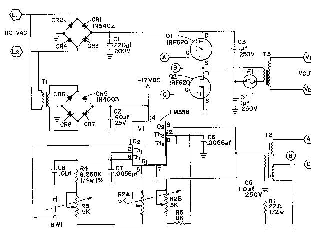
Referring to Fig. 2, the detailed electrical
operation of the preferred embodiment of the present
invention will be described. The 110VAC 60Hz mains
supply is provided on lines Ll and L2 in the upper left
of Fig. 2. The primary operating current is rectified
through a bridge rectifier comprised of diodes CRl
through CR4. The resultant direct current is filtered
by bulk capacitor Cl which in the preferred embodiment
13162~0
--6--
is 220 microfarads. Direct rectified line voltage off
AC mains is typically 160VDC peak. The DC voltage
stored in capacitor Cl and continuously supplied from
the AC mains is applied to the primary of main power
transformer T3 through capacitors C3 and C4 and tran-
sistors Ql and Q2. These capacitors along with the
input inductance seen by the primary on power trans-
former T3 form a resonant converter circuit which
switches the DC power through to the secondary of step-
up power transformer T3. The resultant switched currentis applied through the output terminals Vl and V2 to the
discharge tube for exciting the gas therein. As is
understood by those skilled in the art, the impedance of
the discharge tube attached to the terminals Vl and V2
will affect the impedance seen at the primary of trans-
former T3 and thus will affect the optimal power
transfer point based on the switching frequency of the
resonant converter. Thus, depending upon the impedance
attached to terminals Vl and V2, the optimal switching
frequency must be selected to effect the best possible
power transfer. By varying the switching frequency, the
output voltage Vout may be varied between 4KV-15KV,
depending upon the impedance of the discharge tube
attached between Vl-V2.
The voltage switched through the resonant con-
verter on power transformer T3 is switched through power
MOSFETs Ql and Q2. These transistors in the preferred
embodiment are Part No. IRF620 available from Inter-
national Rectifier and other vendors~ The gates of
these MOSFETs are controlled such that neither MOSFET is
on at the same time. The alternating switching of the
gates of transistors Ql and Q2 vary the direction of the
current through the primary of power transformer T3.
The alternate switching of transistors Ql and Q2 cause a
131~210
--7--
resonant current to develop in the primary which is in
turn transferred to the secondary and on to the
discharge tube 110. Control of the power MOSFETs Ql and
Q2 is effected by the switching control circuit shown in
the lower half of Fig. 2.
In the preferred embodiment of the present
invention, the main controller for establishing the
switching frequencies is by means of a dual timer cir-
cuit, Part No. LM556 available from National
Semiconductor, Signetics, and a wide variety of other
vendors. This LM556 timer circuit contains two indivi-
dual 555-type timers which form the timing control
mechanisms for establishing the switching frequencies.
The supply voltage for driving the 556 timer
Ul is by means of a DC supply circuit connected to the
AC mains. The control supply transformer Tl is attached
across lines Ll and L2 of the AC mains and serves to
step down the AC mains voltage to approximately 20VAC
which is applied to a full-wave rectifier bridge
comprised of diodes CR5 through CR8. The resultant rec-
tified pulsed DC voltage is filtered by capacitor C2
which is in the preferred embodiment a 40-microfarad
capacitor. The resultant 17VDC low-voltage supply is
applied between pins 14 and 7 of the timer circuit Ul.
The dual 556 timing circuits are each operable
in oscillator mode in which the frequency and duty cycle
are both accurately controlled with external resistors
and one capacitor. By applying a trigger signal to the
trigger input, the timing cycle is started and an inter-
nal flip-flop is set, immunizing the circuit from any
further trigger signals. The timing cycle can be
interrupted by applying a reset signal to the reset
input pin. Those skilled in the art will readily
recognize that a wide variety of timing circuits may be
131621Q
--8--
substituted for the type described here. For example,
monostable multivibrator circuits, RC timing circuits,
microcontroller or microprocessor circuits may be
substituted therefor without departing from the spirit
5 and scope of the present invention. The use and selec-
tion of the 556 timing circuit in the present applica-
tion is only one of a variety of preferred
implementations.
The dual timer circuits of integrated circuit
Ul are controlled with the discrete components shown in
Fig. 2 following manufacturer's suggestions for the use
of the 556. Variable resistors R2A and R2B are ganged
together and control the oscillation frequencies of the
timers. The frequencies of the timers are fixed and
move together as the user changes resistor R2
(corresponding to ~nob 106 shown on the supply 100 of
Fig. 1). Variable resistor R3 is used to control the
mixing point of the two frequencies (corresponding to
knob 108 on the supply 100 of Fig. 1). The mixing point
of the two frequencies results in a pulse modulation
effect in the final mixed output frequency.
Timing capacitor C7 is connected to the
threshold and trigger inputs to the first timer (pins 2
and 6, respectively) in the LM556 timer chip U1. Also
connected to the threshold and trigger inputs is the
series resistance comprised of variable resistor R2A,
variable resistor R3, and fixed resistor R4. This R-C
combination determines the frequency of operation of the
first oscillator.
The output of the first oscillator is fed
through capacitor C8 to the control input (pin 11) of
the second oscillator circuit. The trigger and
threshold inputs (pins 8 and 12 respectively) of the
second oscillator circuit are connected to timing capa-
131621~
cltor C6. The series resistance comprised of variable
resistor R2B and fixed resistor R5 provide the discharge
path for capacitor C6. Together, this R-C combination
determines the timing frequency of the second oscilla-
tor. The frequency of oscillation of the second
oscillator is interrupted by the frequency of oscilla-
tion of the first oscillator circuit through the control
input (pin 11) for the second oscillator.
The resulting output frequency on output pin 9
is a pulse modulation mixed frequency used to drive the
primary of control transformer T2. The output pulses on
pin 9 of chip Ul are passed to the primary of control
transformer T2 and find their path to ground through
series capacitor C5 and resistor Rl. Thus, whenever the
output on pin 9 changes state, a small positive-going or
negative-going current spike will appear in the primary
of control transformer T2. This control signal on the
primary is reflected on the control windings of the
secondary which are used to control power MOSFETs Ql and
Q2 which ultimately control the switching of the high
voltage DC into the power output transformer T3.
The construction of transformers Tl, T2 and T3
shown in Fig. 2 are within the skill of those practicing
in the art. Transformers Tl and T2 are commonly
available transformers or they may be specially
constructed according to the specific application of
this device. Control transformer T2 in the preferred
embodiment is a 70-turn primary with two 100-turn
secondaries, creating a 0.7:1.0 transfer ratio. The
primary and secondaries are wound using 36-gauge wire on
a common core and bobbin. Power transformer T3 is of a
more exacting construction due to the high voltage
multiplication on the secondary. The primary is
constructed with 75 turns of #20 single insulated
1316210
--10--
stranded wire wound around a high voltage isolation ccre
very similar to those used in the flyback transformers
of television sets. The secondary is wound on a high
isolation core comprised of 4,000 turns of #34 wire.
The secondary is separated into a plurality of segmented
windings to reduce the chance of arcing between win-
dings and allows operation at higher frequencies by
reducing the capacitance between the windings. For
example, the secondary could be segmented into 6-8
separate windings separated by suitable insulation to
prevent arcing and potted in commonly available insu-
lating plastic to minimize arcing.
In operation, the power supply of Fig. 2 is
attached to the AC mains through lines Ll and L2. A gas
discharge tube is attached between the output terminals
V1 and V2 of power transformer T3. For initial setup,
variable resistor R3 is turned fully counterclockwise
and the ganged switch SWl connected to variable resistor
R3 is in the open position. Thus, during initial setup,
with switch SWl open, the operating frequency of the
first oscillator cannot affect the control input (pin
11) of the second oscillator circuit. In this fashion,
the output voltage controlling the brightness selected
by the main operating frequency of the second oscillator
can be tuned first by tuning R2 before attempting to
eliminate or enh~ance the bubble effect by tuning R3.
With switch SWl open and control R3 at the
fully counterclockwise position, variable resistor R2 is
tuned to create the optimal switching frequency for
controlling switching transistors Ql and Q2 which result
in the optimal output voltage or preferred brightness in
the discharge tube attached to the secondary of power
transformer T3. When the correct voltage or brightness
setting is selected, a bubble effect may or may not be
1316210
seen in the discharge tube. To enhance or reduce the
bubble effect, variable resistor R3 iS turned clockwise
to close switch SWl and to change the mixing point of
the frequencies of oscillators 1 and 2 of timer circuit
Ul.
The preferred embodiment of the present inven-
tion is designed such that a short between the outputs
Bl and B2 can be maintained indefinitely without causing
damage to the supply. If, however, supply 100 is
energized with no load placed between Bl-B2, the output
voltage will tend to run away due to an infinite impe-
dance on the secondary transformer T3. To prevent over-
voltage runaway, the circuit of Fig. 3 is used to shut
down the oscillator of the timing circuit LM556 when
overvoltage condition is sensed. A commonly available
spark gap can be placed between one of the output lines
and one of the aforémentioned segmented secondary coils,
or may be placed between Bl and B2. The spark gap is
selected for the upper limit of output voltage allowable
at supply 100. When a spark is created on spark gap
301, the light created by the sparking is sensed by pho-
todetector circuit 302. Detector circuit 302 is in the
preferred embodiment and photo-Darlington amplifier,
part No. L14Rl available from General Electric and other
vendors. When activated, photodetector 302 will cause a
current to flow from the +17VDC supply through resistors
R6 and R7 to ground. Current through resistor R6 will
tend to pull the trigger line of SCR 303 high,
triggering the SCR. With an active signal on the
trigger line for SCR 303, current is allowed to flow
from the +17VDC supply through resistor R8 to ground.
As is known by those skilled in the art, once an SCR is
energized, it tends to remain energized until current
through the SCR is removed. Thus, a latching function
1 3 1 62 1 ~1
-12-
is created, disabling the supply 100 until it is
deenergized to reset SCR 303. When SCR 303 is
energized, current is drawn from pin 12 of the LM556
timing circuit through diode Dl onto ground. The
grounding of pin 12 effectively shuts down all the
timing functions and stops the oscillation through
transformer T3.
While the present invention has been described
in connection with the preferred embodiment thereof, it
will be understood that many modifications will be
readily apparent to those of ordinary skill in the art,
and this application is intended to cover any adap-
tations or variations thereof. Therefore, it is mani-
festly intended that this invention be limited only by
the claims and the equivalents thereof.