Note: Descriptions are shown in the official language in which they were submitted.
1 - 1 3 1 6 2 2 '
FIELD OF THE INVENTION
, .
The present invention relates to a TM mode
dielectric resonator in which a solid internal dielectric
column is provided inside a cavity case, with both column
and cavity case being made of a high frequency ceramic
dielectric material. The present invention also relates to
a method for manufacturing such a TM mode dielectric resona-
tor.
BRIEF DESCRIPTION OF THE DRAWINGS
Objects and features of the present invention
will become apparent from the following description taken
in conjunction with a preferred embodiment thereof with
reference to the accompanying drawings, throughout which
like parts are designated by like reference numerals, and
in which: ~
- Fig. 1 is a perspective view of a dielectric
resonator according to a preferred embodiment of the present
invention;
Fig. 2 is a cross-sectional view taken along a
line II-II shown in Fig. 1;
Fig. 3 is a cross-sectional view showing one
example of a mold used for injection molding to make the
dielectric resonator of Fig. l;
; Fig. 4a is a diagrammatic view of molding appara-
tus to make the dielectric resonator of Fig. l;
- 2 1 31 622,
Fig. 4b is a block diagram showing the steps for
manufacturing the dielectric resonator of Fig. l;
Fig. 5 is a cross-sectional view showing a conven-
tional dielectric resonator; and
Fig. 6 is a cross-sectional view showing another
conventional dielectric resonator.
DESC~IPTION OF THE Pi~IOR ART
_
Conventional dielectric resonators of this type
provide an internal dielectric column made from a dielectric
ceramic is installed inside a cylindrical cavity case
manufactured by bonding ceramic plates with a binder. The
top and bottom ends of this internal dielectric column are
bonded to the inside wall,of the cavity case, and a conduc-
tive film which is for the real current path is formed on
the inside wall or the outside wall of the cavity case by
silver baking or other processes.
A ceramic cavity case is use~ instead of a metal-
lic cavity case for the following reasons. If an internal
dielectric column made of a dielectric ceramic is installed
inside a metallic cavity case and bonded to the inside wall
of the metallic case with a silver paste applied to the top
and bottom ends of the internal dielectric column, the
differences in the coefficients of thermal expansion of the
metallic case and internal dielectric column result in
~,
~ 3 ~ 1 3 1 6 2 2 7
separation between the inside wall of the metallic case and
the top and bottom of the internal dielectric column. Once
separation occurs, the resulting joule loss causes the Q
factor of the filter to drop, and thus causes problems of
instability in the filter characteristics. Therefore, the
cavity case is formed from a ceramic material with approxi-
mately the same coefficient o~ thermal expansion as the
internal dielectric column. A conductive film is then
formed on the surface of the cavity case to carry the real
current.
A cross section of a conventional dielectric
resonator is shown in Fig. 51 in which the cavity ca6e is
formed from a ceramic material. In this dielectric resona-
tor 5, a silver paste is applied to the inside surfaces of
ceramic top 6, bottom 7, and sides 8. When this silver
paste is baked with top 6, bottom 7,~and sides 8 assembled
as shown, the silver acts as a binder and members 6, 7, 8
are bonded together to form a square-shaped cavity case 9
while at the same time forming conductive film 10, which
forms the real current path, on the inside walls of cavity
case 9. In a separate process, a silver paste is also
applied to the top and bottom ends of internal dielectric
column 11 prepared separately. Internal dielectric column
11 is then placed inside cavity case 9, and by baking the
silver paste on both ends of internal dielectric column 11
to conductive film 10 inside cavity case 9, the top and
..~
- 4 - 1 3 1 6227
bottom ends of internal dielectric column 11 are affixed to
the inside wall of cavity case 9.
However, in processes in which a silver paste is
applied to both ends of internal dielectric column 11 and
baked to cavity case 9, the end processing of internal
dielectric column 11 to which the paste is applied is time
consuming, and the baking conditions are strict. Thus,
technically it is difficult to expect complete bonding
between internal dielectric column 11 and cavity case 9.
Also, if the bond between cavity case 9 and internal
dielectric column 11 is not complete, incomplete bonded
areas will temporarily contact and separate, causing unsta-
ble electrical conductivity between internal dielectric
column 11, which i8 the displacement current path, and
conductive film 10, which is the real current path. Thus,
noise will easily occur and the filter characteristics will
not be stable.
Another conventional embodiment is shown in Fig.
6. In this dielectric resonator 15, top 6, bottom 7, and
sides 8 are bonded by means of glass glaze 12 to form square
cavity case 13. The top and bottom ends of internal
dielectric column 11 placed inside cavity case 13 are also
bonded to the inside walls of cavity case 13 by means of
glass glaze 12 applied to both ends. A silver paste is then
applied to the outside walls of cavity case 13 and baked to
form conductive film 14.
- 5 - 1 31 6227
However, because the dielectric constant of glass
glaze 12 is low, and the intrinsic conductivity is low and
the Q factor is low, the Q factor of the dielectric resona-
tor 15 also drops due to the effect of the low Q factor
glass glaze 12 interposed between internal dielectric column
11 and conductive film 14. Furthermore, due to variations
in the thickness of the glass glaze 12 (the dielectric
constant of glass glaze 12 is relatively low compared with
that of internal dielectric column 11), the bulk dielectric
constant of the bond sites of internal dielectric column 11
and cavity case 13 is varied. Thus, the variation in the
dielectric constant causes significant errors in the reso-
nance frequency of dielectric resonator 15.
Moreover, in each of the conventional members
described above, because the dielectric resonator is formed
b~ bonding top 6, bottom 7, sides 8, and internal dielectric
column 11 together by means of a silver paste, glass glaze,
or other binder, additional time and processes are required
in manufacturing for assembly, thereby increasing manufac-
turing costs.
SUMMAR~ OF THE INVENT~ON
The present invention has been developed with a
view to substantially solving the above described disadvan-
tages and has for its essential ob~ect to provide an im-
proved dielectric resonator which operates with high stabil-
ity and high reliability, and with which uniform, constant
resonator characteristics can be obtained.
13162~7
6 -
Also, it is an important object of the present
invention to provide a method for manufacturing such an
improved dielectric resonator to simplify the manufacturing
process and also to reduce production costs.
In accomplishing these and other objects, a
dielectric resonator according to the present invention
comprises: a cavity case made of ceramic material and having
top and bottom walls and one pair of side walls extending
between the top and bottom walls to define a cylindrical
cavity; a solid internal dielectric column made of ceramic
material and having its opposite ends monolithically con-
nected to the top and bottom walls; and an electric conduc-
tive film formed on the surface of the cavity case for
carrying a real current.
Also, according to the present invention, a method
for manufacturing a dielectric resonator comprises the steps
of: molding a dielectric resonator body which comprises a
cavity case made of ceramic material and having top and
bottom walls and one pair of side walls extending between
the top and bottom walls to define a cylindrical cavity, and
a solid internal dielectric column made of ceramic material
and having its opposite ends monolithically connected to the
top and bottom walls; sintering the molded dielectric
resonator body; and depositing an electric conductive film
on the surface of the cavity case which is capable of
carrying a real current.
............
_ 7 _ 1 31 6227
In a dielectric resonator according to the present
invention, the ends of the internal dielectric column are
integrally formed with the inside wall of the cavity case
without the use of a binder intermediate. Thus, the con-
necting condition between the internal dielectric column and
the cavity case is stable both mechanically and electrical-
ly, and therefor, there are no problems with the separation
of the bond site or poor bonding. Thus, a resonator with
high reliability can be obtained. Specifically, a stable
resonance frsquency can be obtained because noise is not
generated in the output by an unstable bond site as occurred
in conventional dielectric resonators bonded by baking a
silver paste, and a drop in the Q factor and variations in
the resonance frequency do not occur as in conventional
dielectric resonators bonded with a glass glaze.
Furthermore, the manufacturing method for a
dielectric resonator according to the present invention
makes it possible to obtain a dielectric resonator as
described above, to simultaneously mold the internal
dielectric column and the cavity case by an in~ection
molding or other monolithic molding process. ThuQ, with the
present invention, the number of processes required for
manufacturing is decreased by eliminating the cavity case
and internal dielectric column assembly processes, resulting
in the reduction of manufacturing costs. In addition, the
manufacturing method according to the present invention is
also suited to mass production by eliminating the assembly
~,~r, '
process.
1 31 6227
-- 8 --
DETAILED D~SCRIPTION OF THE PREFERRBD EMBODIMENT
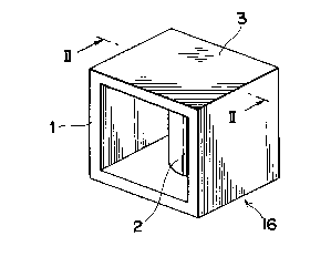
Referring to Figs. 1 and 2, dielectric resonator
16 according to a preferred embodiment of the present
invention includes a solid internal dielectric column 2
placed inside a hollow cylindrically-shaped cavity case 1.
Cavity case 1 has top and bottom walls to which internal
dielectric column 2 is integrally connected, and one pair of
side walls. Thus, internal dielectric column 2 can be seen
from another side of cavity case 1. A silver paste is baked
to the outside surface of cavity case 1 to form conductive
film 3. A TMo1o mode dielectric resonator 16 is thus
constructed so that internal dielectric column 2 becomes the
displacement current path and conductive film 3 becomes the
real current path.
The cavity case 1 and internal dielectric column 2
are formed monolithically from a titanium oxide or other
ceramic material with a high dielectric constant. Since a
silver paste or glass glaze is not interposed between the
top and bottom ends of internal dielectric column 2 and the
inside wall of cavity case 1, internal dielectric column 2
can be firmly installed in cavity case 1. In other words,
when body is e~ected from the mold, cavity case 1 and
internal dielectric column 2 are molded monolithically so
that internal dielectric column 2 is bonded continuously and
homogeneously to cavity case 1.
As shown in Figs. 1 and 2, internal dielectric
column 2 is molded as a round column, but it may also be
g t3162~7
molded as a column with a square or other cross section.
Furthermore, as shown in Fig. 2, conductive film 3 is
provided only on the outside surface of cavity case 1, but
it may also be provided on the inside wall of cavity case 1
or on all surfaces of cavity case 1.
In a dielectric resonator 16 so constructed, the
displacement current flowing through internal dielectric
column 2 is converted to a real current between internal
dielectric column 2 and conductive film 3 and flows to
conductive film 3, and the specific electromagnetic vibra-
tions of the TMo10 mode are trapped inside cavity case 1.
Furthermore, by mounting multiple dielectric resonators 16
inside a metallic case (not shown in the figures) and
electrically connecting the conductive films 3 of ad~acent
dielectric resonators 16 by means of a common ground plate
(not shown in the figure), a specific electromagnetic
coupling occurs between adjacent dielectric resonators 16,
and the assembly can be used as a multistage dielectric
filter.
A manufacturing method for making dielectric
resonators according to the present invention is described
next with reference to Figs. 4a and 4b.
Referring to Fig. 3, a molding machine comprises
molds 17a and 17b which are used for one-step monolithic
molding of cavity case 1 and internal dielectric column 2 by
an in~ection molding process. While only one molding cavity
18 is shown in Fig. 3, a mold 17a, 17b for injection molding
1 31 6227
-- 10 --
with which multiple dielectric resonators can be molded at
one time can be made by providing multiple molding cavities
18. Molding cavity 18 is formed in mold 17a, 17b for
injection molding to simultaneously mold cavity case 1 and
internal dielectric column 2. A parting face PL is provided
so as to pass through the center of internal dielectric
column 2.
Referring to Fig. 4a, a bulk powder of ~itanium
oxide or other high dielectric constant ceramic material to
which an organic binder for molding has been added is then
charged from hopper 20 of in~ection molding machine 19, and
the in~ection plunger inside in~ection molding machine 19 is
driven ~o in~ect the molding material into molding cavity 18
of mold 17a, 17b to simultaneously and monolithically mold
body 4 of cavity case 1 and internal dielectric column 2.
After this, one side of the mold, mold 17a, is moved using
air cylinder 21 connected to mold 17a, the movable side of
the mold, and molds 17a and 17b are separated and opened
from parting face PL to e~ect the ceramic body 4. An
e~ected body in which the top and bottom ends of internal
dielectric column 2 are monolithically bonded to the inside
wall of cavity case 1 is thus obtained.
Referring to Fig. 4b, treatment steps are shown.
After the organic binder for molding is removed in degreas-
ing process 22, body 4 is sintered to a hard, dense ceramic
molding in sintering process 23. ~herefore, cavity case 1
and internal dielectric column 2 have a uniform structure
1 31 62~1
11 --
throughout, and the bond site of the two members in
particular is a uniform structure stable both mechanically
and electrically. After sintering, a silver paste is
applied to the outside surface of cavity case 1 by coating
machine (not shown) at a silver coating process 24, and this
silver paste is baked by oven (not shown) at baking process
25 to form conductive film 3 on the surface of cavity case
1.
In the manufacturing method as described above,
the cavity case and internal dielectric column are simulta-
neously and monolithically molded by an injection molding
proces~, but a similar monolithic molding can also be
achieved by compression molding, transfer molding, and other
molding processes. Moreover, it is also possible to mold a
cylindrical cavity case body and an internal dielectric
column body separately, bond by means of press fitting or
other method the top and bottom ends of the internal
dielectric column to the inside walls of the cavity case
while both moldings are still in a body state, and then
monolithically sinter the cavity case and internal
dielectric column bodies together to form a monolithic
dielectric resonator without using a binder to bond the
cavity case and internal dielectric column.
According to the present invention, a high reli-
ability dielectric resonator which is stable mechanically
and electrically at the bond site between the internal
dielectric column and the cavity case can be obtained.
1 31 6221
- 12 -
Furthermore, such problems of conventional dielectric
resonators as the generation of noise due to an unstable
bond site between the internal dielectric column and the
cavity case, a decrease in the Q factor such as occurs when
a binder with a low specific conductivity is used, and
variations in the resonance frequency such as occur when a
binder with a dielectric constant different from that of the
internal dielectric column is used, can be resolved. Fur-
thermore, by manufacturing a dielectric resonator using the
method according to the present invention, the cavity case
and internal dielectric column can be simultaneously molded
a~ a monolithic structure, the process of assembling the
cavity case and internal dielectric column can be eliminat-
ed, the production process can be simplified, the production
cost of dielectric resonators can be reduced, and dielectric
resonators can be easily mass produced.
Although the present invention has been fully
described in connection with the preferred embodiment
thereof with reference to the accompanying drawings, it is
to be noted that various changes and modifications are
apparent to those skilled in the art. Such changes and
modifications are to be understood as included within the
scope of the present invention as defined by the appended
claims unless they depart therefrom.