Note: Descriptions are shown in the official language in which they were submitted.
1316231
CHIP RESISTOR
BACKGROUND OF THE INVENTION
1. FIELD OF THE INVENTION
This invention relates to the fabrication of
thick film resistors for use in hybrid microcircuits
and more particularly, to a method of forming
dielectric material on a substrate material during the
fabrication of the thick film resistors and subsequent
removal of the thick film resistors from the carrier
substrate.
2. DESCRIPTION OF THE RELATED ART
Various techniques for the fabrication of thick
film resistors have been proposed in the past. Thick
film resistors have been in use in the electronics
industry for more than the past 20 years. One typical
application has been to use the thick film resistor in
conjunction with a conductor network in a hybrid
circuit. Recently, many users of such device have
directed development activities toward the making and
use of pick-and-place technology to fabricate the
hybridized circuitry. The resistors currently being
evaluated for most of these applications are typically
cermet chip resistors. These resistors are in effect
separate thick circuits consisting of one resistor
terminated with a conductor.
l 3 l 62~ '~
SUMMARY OF THE INVENTION
The present invention proposes a thick film chip
resistor constructed of two layers: a carrier
substrate and a ceramic adhesive (ceramic substrate)
with the conductors superimposed either above or below
the resistive material on top of the ceramic
substrate. The particular technique and materials
utilized in the present process of making chip
resistors effectively takes advantage of that
condition, wherein the ceramic adhesive material loses
its adhesion to the metal substrate during the material
processing cycle. Thus, the metal carrier substrate
can be disposed of, leaving a resistor fabricated upon
a ceramic substrate which readily adapts itself to the
utilization in hybrid technology.
Thus, in view of the foregoing difficulties with
the prior art, it is an object of the present invention
to provide a chip resistor having a simplified
manufacturing process which facilitates the
pick-and-place technology used for the construction of
hybrid conductive networks.
It is another object of the invention to provide
a chip resistor having a thick film resistor which can
be produced by a simple way without detriment to the
adhesive characteristic of the thick film resistor.
It is still another object of the invention to
provide a chip resistor which can easily be connected
to a hybrid circuit unit by a simple mass-produced
soldering technique.
BRIEF DESCRIPTION OF THE DRAWINGS
FIG. 1 is a sectional view of a prior art thick
film resistor viewed in cross-section as fabricated
within a circuit.
FIG. 2 is a typical cross-section of a prior art
chip resistor.
1 31 6231`
FIG. 3 is a cross-sectional view of a chip
resistor in accordance with the present invention.
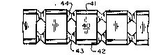
FIG. 4 is a top view of a plurality of resistors
constructed in accordance with the methods set forth in
the present invention.
FIG. S is a side view of a plurality of
resistors constructed in accordance with the methods
set forth in the present invention.
DETAILED DESCRIPTION
In one prior art arrangement the structure of
the resistors is like that illustrated in FIG. 2, and
consists of an alumina substrate 23 on which is located
a resistor coating 20, a first conductor such as 22
located in contact with the resistive material 20 and
second edge mounted conductor 24 connected thereto and
the resistive material 20 and first conductor 22 is
covered by glass encapsulant 21. A comparison of this
type of resistor to that of a typical thick film
resistor, which consists of an alumina substrate 13 on
which are formed conductors, such as conductor 12 in
contact with resistive material 10 and with a glass
encapsulant material 11 superimposed over the resistive
material, as shown in FIG. 1, will show only the
addition of the edge conductor 24. The prior art
techniques exhibit a number of drawbacks, including
high cost, the fabrication, difficulty in mounting and
establishing appropriate electrical connections to the
unit. Many of the techniques proposed require
inefficient manual soldering operations for a
connection, while others, in an attempt to accommodate
dip soldering or reflow soldering techniques, use such
uneconomical techniques as vacuum, electron beam
evaporation or sputtering to achieve devices where a
connection can be made by dip soldering or reflow
soldering.
.,
l 3 l 623 I `
In yet another instance, films may be deposed by
printing metal qlaze paste or by similar means and then
the films are fired to form lateral electrodes. The
high temperature of the firing operation called for
thlls causes deterioration of the low resistance
temperature coefficient of the resistor and the high
stability of the resistives which characterize the
resistor.
Referring now to FIG. 3, an alumina or other
metallic substrate 33 is employed as a carrier or
support device during construction of thick film
resistors as taught in the present invention. Upon
this carrier substrate, an adhesive layer 35 of a
ceramic adhesive dielectric material, such as the
No. 481 adhesive manufactured by the Sermetel Materials
Division of Teleflex Incorporated is placed. This
material is either brushed or screened on after which it
1 31 G~3'
84-4-052-CIP
is heated to a temperature of 315 degrees centigrade in an
~ir atmosphere for a period of approximately one hour.
After this, the resistive material 30 may be applied to
the dielectric material 35 which is now ~f sufficient
thickness and rigidity after baking 90 that it will
support the chip resistor. The resistive material 30 will
now be applied to the ceramic substrate by screen-printing,
spraying or any other well-known technique utilized by those
skilled in the art. At the completion of the application of
the resistive material, the resultant assembly will be
heated for ten minutes at a temperature of approximately 150
degrees centigrade to eliminate any organic component
pre~ent in the resistive material 30.
After this ~tep i9 completed, conductors 32 may be
applied by any of the similar techniques to those utilized
for the application of the resistive material 30, after
which heating for ten minutes, at approximately 150 degrees
centigrade takes place to eliminate any organic component
present in the conductive material 32. While it is
preferred that the resistive materials 30 be processed prior
to the conductive material 32, it is quite possible for
the conductors 32 to be printed first, after which the
resistive material 30 would be applied over the conductive
material 32 with the appropriate heating steps included in
between.
It should be noted that the temperatures at which the
1 31 6 ~ 3 ` 84-4-052-CIP
heating initially of the adhesive material 35 and the
subsequent heating of the resistive 30 and cvnductive
materials 32 takes place are substantially below 704 degrees
centigrade, which is the temperature at which, when the
ceramic dielectric 35 is fired, it will lose most of its
adhesion quslity to the supporting metallic carrier
substrate 33. After the resistive material and the
conductive material has been applied and heated, the entire
assembly would be fired for approximately one hour in an air
atmosphere at a temperature reaching 850 degrees centigrade
for a period of ten minutes and then allowed to cool.
After this final firing step, the dielectric 35 loses
most of its adhesion quality and the resi~tor is thus
released from the carrier sub~trate 33 with the application
of only minimum additional force. It should be then noted
that during construction of at least one embodiment of the
present invention, numerous screen printable or sprayable
thick film resistor compositions may be used for the
resistive portion 30, while numerous thick film conductive
inks may be utilized for the conductor.
Utilization of a dielectric adhesive 35 as a substrate
material permits the printing of resistors of various sizes.
Ina~much as the resistors will at least partially self-
release during the processing cycle. There is no need for
- 25 the usual requirement of laser scribing to separate the
resistors from the base material. It is also suggested that
;
1316231
84-4-052--GIP
a bar of dielectric material 44 and 54 may be printed between
individual resistors as shown in FIGs. 4 and 5 with fracture
points designated at locations like 43, as shown in FIG. 4,
and 53, as shown in FIG. 5.
An alternate option for use in the design of resistors
in accordance with the present invention would be to
incorporate the use of an organic conductive material to dip
the edges of the resistors to allow for side terminations.
The concept of using an adhesive to adhere chip
resistors to a carrier substrate during processing is not
necessarily limited as in the present invention to the high
temperature cermet materials. The concept may also be
incorporated into the fabrication of chip resistors using
organic material~ where the dielectric may be a
nonconductive epoxy.
While but a particular embodiment of the present
invention has been shown, it will be obvious to those
skilled in the art that numerous modifications of the
` present invention may be made without departing from the
spirit of the present invention, which shall be limited only
by the scope of the claims appended hereto.