Note: Descriptions are shown in the official language in which they were submitted.
1 31 625q
The present invention relates generally to a
sound reproducing apparatus, and more particularly, to a
sound reproducing apparatus for continuously deriving a
sound signal reproduced from a sound recording media such
as a tape at a speed at the time of recording in a special
reproduction mode such as a so-called review reproduction,
in an apparatus having at least a sound reproducing
mechanism such as a video tape recorder and an audio tape
recorder.
In general, in an apparatus having at least a
sound reproducing mechanism such as a video tape recorder
or an audio tape recorder, there exists a special
reproducing mechanism such as a review mechanism for
accessing a desired position to be reproduced by
reproducing a sound signal while travelling a tape (having,
for example, the sound signal recorded thereon) at high
speed in the direction opposite of the normal reproduction
mode.
1 31 625q
However, when the sound signal is reproduced by
such a review mechanism, the sound signal is reproduced in
reverse, so that the meaning of sound can not be grasped.
In addition, since the reproduced sound signal is time-
5 base-compressed, the frequency thereof is high, so that it
is more difficult to confirm the content thereof.
In order to solve this problem, a technique has
been proposed in which in the above described review
reproduction, a reproduced sound signal is stored in a
memory at a speed proportional to a review reproducing
speed, and after storing is completed, the reproduced sound
signal is read out from the memory while being time-base-
expanded to derive the same at the original speed, which is
disclosed in, for example, Japanese Patent Laying-Open
Gazette No. 45607/1984.
However, according to such a technique,
derivation of the sound signal is interrupted while the
reproduced sound signal is being written into the memory.
Therefore, the reproduced sound signal is always written in
a memory to and from which writing and reading can be
performed in parallel at the speed corresponding to the
tape speed while being read out from the memory in the
order opposite to that in writing. However, since the
writing speed of the
.
1 31 625q
reproduced sound signal is fast and memory capacity is
limited, in which the reproduced sound signal read out from
the memory is continuous, is shortened. More specifically,
the sound signal to be derived becomes a sound signal
having many discontinuous portions. If the memory capacity
is increased, such a problem can be solved. However, there
is an associated increase in cost as a result.
Therefore, an advantage of the present invention
is the provition of a sound reproducing apparatus capable
of continuously deriving a sound signal of a considerable
length even during reverse reproduction such as review
reproduction.
Another advantage of the present invention is the
provision of a sound reproducing apparatus capable of
deriving a reproduced sound signal even in a special
reproduction mode without requiring an increased memory
size.
Briefly stated/ a sound reproducing apparatus
according to the present invention includes a circuit for
scanning a recording media having at least a sound signal
recorded thereon at a predetermined recording speed, in the
direction opposite to that at the time of recording at a
reproducing speed N (N: positive integer) times the
predetermined recording speed to produce the sound
1 31 625q
signal; a memory to and from which a digital signal can be
written and read out; a read address generating circuit
îor generating a read address signal changed in one
direction in a predetermined cycle for speci~ying an
address at which the digital signal is to be read out from
the memory; a circuit for generating address information
changed in the direction opposite to that of the read
address signal at a speed N times that o~ the read address
signal; a write address generating circuit for supplying
the above described address information as a write address
signal for specifying an address at which the digital
signal is to be written to the memory in a cycle
corresponding to N/(N+1) times the predetermined cycle of
the read address signal and only during a first period
corresponding to 1/(N+1) times the above described
predetermined cycle of the read address signal; an address
selecting circuit for supplying the read address signal to
the-memory when the read address signal is generated and
supplying the write address signal to the memory when the
write address signal is generated in the first period;
circuit for converting the sound signal reproduced by the
reproducing circuit into a digitzl signal at a first speed
proportional to the reproducing speed and writing the same
to the address specified by the write address signal in
the memory; and a circuit for reading out the digital
~s ;~.
., ,
1 3 1 6 L. 5 ~
sound signal from the address specified by the read
address signal in the ~emory at a second speed
proportional to the recording speed and converting the
same into an analog signal.
In accordance with another aspect of the present
invention, the sound reproducing apparaius~:includes- a
circuit for scanning a recording media having at leas. a
sound signal recorded thereon at a predetermined recording
speed, in the same direction as that at the time of
recording at a reproducing speed of one-half of the
predetermined recording speed to reproduce a sound signal;
a memory to and from which a digital signal can be written
and read out; a read address generating cixcuit for
generating a read address signal changed in one direction
in a predetermined cycle for specifying an address at
which the digital signal is to ~e read out from the
memory; a write address generating circuit for generating
a write address signal changed in the same direction as
that of the read address signal in synchronization with
the initiation of the change in the read address signal
and in a cycle two times the predetermined cycle of the
read address signal for specifying an address at which the
digital signal is to be written to the memory; an address
selecting circuit for supplying the read address signal to
the memory when the read address signal is generated and
1 31 625~
supplying the write address signal to the memory when the
write address signal is generated; a circuit for
converting the sound signal reproduced by the reproducing
circuit into a digital signal at a first speed
proportional to the reproducing speed and writing the same
to the address specified by the write address signal in
the memory; and a circuit for reading out the digital
sound signal from the address speciried by the read
address signal in the memory at a second speed
propor,ional to the recording speed and converting the
same into an analog signal.
In accordance with still another aspect of the
present invention, the sound reproducing apparatus
includes a circuit for scanning a recording media having
at least a sound signal recorded thereon at a
predetermined recording speed, in the same direction as
that at the time of recording at a reproducing speed two
time the predetermined recording speed to reproduce the
sound signal; a memory to and from which a digital signal
can be written and read out; a read address generating
circuit for generating a read address signal changed in
one direction in a predetermined cycle for specifying an
address at which the digital signal is to be read out from
the memory; a circuit for generating address information
changed in the same direction as that of the read address
;.......................................... - 6 -
.:
1 31 6~5q
signal at a speed two times that or the read address
signal; a write address generating circuit }or supplying
the address information as a write address signal ror
specifying an address at which the digital signal is to be
written to the memory in a cycle two times the
predetermined cycle of the read address signal and only
during a first period corresponding to the predetermined
cycle of the read address signal; an address supplying
circuit for supplying the read address signal to the
memory when the read address signal is generated and
supplying the write address signal to the memory when the
write address signal is generated in the first period; a
circuit for converting the sound signal reproduced by the
reproducing circuit into a digital signal at a first speed
15 proportional to the reproducing speed and writing the same
; to an address specified by the write address signal in the
memory; and a circuit for reading out the digital sound
signal from the address specified by the read address
signal in the memory at a second speed proportional to the
20 recording speed and converting the same into an analog
signal.
Thus, a principal advantage of the present invention
is that the reproduced sound signal is written to the
memory with the address being reversed at a speed N times
25 the recording speed in a period 1/(N+1) times the cycle of
_ 7 --
1 31 6259
the read address signal, and the sound signal as written
is continuously read out in a cycle N/(N+l) times the
above described cycle or the read address signal, so that
the reproduced sound signal or a considerable length can
be derived without interruption even during reverse
reproduction.
The foregoing and other objec~s, features, aspects
and advantages of the present invention will become more
apparent from the following detailed description of the
present invention when taken in conjunction with the
accompanying drawings.
BRIEF DESCRIPTION OF THE DRAWINGS
Fig. 1 is a schematic block diagram showing a sound
reproducing apparatus in a video tape recorder according
to one em~odiment of the present invention;
Fig. 2A-C are a timing chart for explaining the
operation of the invention in a reproduction mode in which
a signal is reproduced at a speed ~ive times that in the
normal reproduction mode (referred to as 5 multiple speed
reproduction mode hereinafter) according to the embodiment
shown in Fig. 1;
Fig. 3A-C are a timing chart for explaining the
operation in a 2 multiple speed reproduction mode according
to the embodiment shown in Fig. 1.
1 31 6LJq
Fig. 4A and B are a timing chart for explaining the
operation in a 1/2 multiple reproduction mode according to
the embodiment shown in Fig. 1;
Fig. 5A-C are a timing chart for explaining the
operation in a -5 multiple speed reproduction mode
according to the embodiment shown in Fig. 1; and
Fig. 6A-D are a diagram for explaining timings for
writing and reading to and from a memory in various
reproduction modes shown in Figs. 2 to 5.
DESCRIPTION OF THE PREFERRED ~BODIMENTS
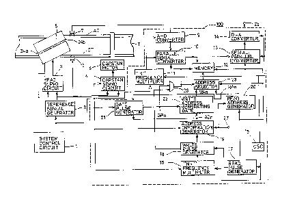
Fig. 1 is a schematic block diagram showing a sound
reproducing apparatus in a video tape recorder (referred
to as VTR hereinafter) having a special reproducing
mechanism such as multiple speed reproduction according to
one embodiment of the present invention.
In the VTR shown in-Fig. 1, a system control circuit
1 generates a mode designating signal for designating
various reproduction modes, to apply the same to a
reference signal generator 2, a capstan servo circuit 4
and a sound signal processor l00. In the embodiment shown
in Fig. l, the modes designated Dy the system control
circuit 1 include a 2 multiple speed reproduction mode, a
5 multiple speed reproduction mode, a 9 multiple speed
reproduction mode, a -5 multiple speed reproduction mode,
a -9 multiple speed reproduction mode and a 1/2 multiple
~ ,.
,~ .
t 31 6259
speed reproduction mode, in addition to a normal
reproduction mode. The mode designating signal includes
information concerning multiple speed anà information
concerning direction. In general, in an +N (N: positive
number) multiple speed reproduction mode, the information
concerning multiple speed indicates the absolute value N
of a number of multiple speed, and the information
concerning direction indicates positive and negative
signs.
In Fig. 1, the reference signal generator 2 generates
a reference signal having a frequency switched in response
to the mode designating signal generated from the system
control circuit 1, to apply the same to a head servo
circuit 3 and the capstan servo circuit a. A cylinder 6,
which has video heads 24a and 24b provided thereon,
generates a rotation detecting signal indicating the
... . _.
rotational speed of the cylinder itself to apply the same
: to the head servo circuit 3. The head servo circuit 3
receives the reference signal applied.from the reference
signal generator 2 and the rotation detecting signal
applied from the cylinder 6 to generate a control signal
for controlling rotation of a cylinder motor (not shown)
in the cylinder 6, so that the video heads 2~a and 2~b are
rotated at a predetermined speed.
-- 10 --
~ ' `' .
131625q
Additionally, a reproduced control signal is obtained
from a control track CT on a video tape T by a control
head 5, to ~e applied to the capstan servo circuit ~. The
capstan servo circuit 4 frequency-divides this reproduced.
control signal in a predetermined ratio and then, compares
in phase the frequency-divided signal with the reference
signal from the reference signal genexator 2, and controls
rotation of a capstan motor 8 at a predetermined speed
determined by the mode designating signal from the system
control circuit 1. As a result, the video tape T is
moved in a designated reproduction mode, so that a
sound signal is reproduced from an audio head 7 scanning
an audio track AT at a speed corresponding to the
travelling speed of the tape.
The following is a description of the sound signal
processor 100 in the VTR shown in Fig. 1. First, the mode
designating signal from the system control circuit 1 is
applied to an "N" frequency multiplier 11, an "N~1"
frequency multiplier 16, an address inform~tion generator
19 and a gate pulse generator 21 in the sound signal
processor 100. Simultaneously, an oscillator (oSC) 15
generates a reference sampling pulse signal of 15 KHz to
:: apply the same to the ~N~ ~requency multiplier 11, a
serial-parallel converter 13 and a D/A converter 14, and
generates a reference clock pulse signal of 90 K~z to
-- 11 --
1 3 1 62 J9
apply the same to the "N+l" frequency multiplier 16 and a
read pulse generator 17. Thus, the "N" frequency
multiplier 11 frequency-multiplies the reference sampling
pulse signal of 15 XHz by N according to the information
concerning multiple speed of the mode designating signal
(for example, when the mode designating signal designates
the S multiple speed reproduction mode, it
frequency-multiplies the reference sampling pulse signal
of 15 KHz by 5, to generate a pulse signal having a
frequency of 75 KHz). An output of the "N" frequency
multiplier 11 is applied to the A/D converter 9 as a A/D
conversion pulse signal, as well as to a parallel-serial
converter 10 as a transfer pulse signal. The A/D
converter 9 receives a sound signal from the audio head 7
~eproduced at a speed proportional to the travelling speea
of the tape T, and converts the same into a 6-bit digital
sound signal at a speed proportional to the travelling
speed of the tape T in response to the A/D conversion
pulse signal and outputs said digital sound to parallel-
serial converter 10. The parallel-serial converter 10
receives the 6-bit digital sound signal in parallel in
response to the transfer pulse signal from the "n"
frequency multiplier 11, to serially supply the same to a
memory 12 in synchronization with write pulses as described
below. Memory 12 is a 256 K-bit random access memory (RAM)
to which data is written in response
- 12 -
1 31 6259
to a write address signal in a write mode and from which
data is read out in response to a read address signal in a
read mode. The serial-parallel converter 13 converts into
data a digital sound signal read out bit by bit from the
memory 12 into 6-bit parallel data in response to read
pulses as described below. The D/A converter 14 receives
the 6-bit parallel data from the serial-parallel converter
13 and converts the same into an analog sound signal in
synchronization with the reference sampling pulse signal of
15 KHz from the oscillator 15, to output the same through
an output terminal 25.
The "N+1" frequency multiplier 16 frequency-
multiplies by (N+1) the reference clock pulse signal of 90
KHz from the oscillator 15 in response to the information
concerning multiple speed of the mode designating signal
(for example, when the mode designating signal designates
the 5 multiple speed reproduction mode, it frequency-
multiplies the reference clock pulse signal by 6). An
output of the "N+1" frequency multiplier 16 is applied to
a write pulse generator 18. The read pulse generator 17
outputs the reference clock pulse signal of 90 KHz from the
oscillator 15 without any modification as read pulses, to
apply the same to the write pulse generator 18, a read
address generator 20, an address selector 23, memory 12 and
the serial-parallel
- 13 -
1 31 62J9
converter 13. The write pulse generator 18 picks out only
pulses synchronized in phase with the read pulses from the
read pulse generator 17 of the output from the "N l"
freauency multiplier 16 thereby to form write pulses, to
apply the same to an address information generator 19 and
one input of an AND gate 26. The address information
generator 19 enters a count moàe by addition when the
information concerning direction of the mode designating
signal applied from the system control circuit l instructs
forward direction reproduction and by subtraction when - -
system control circuit 1 instructs opposite direction
reproduction. The address information generator 19 is
reset by a reset pulse supplied from a signal source (not
shown) through input terminal 27 at the timing of setting
a mode and then, initiates counting by addition or
subtraction of the write pulses from the write pulse
generator 18 thereby forming address information ADn, to
apply the same to the gate pulse generator 21 and a write
address generating gate 22.
The read address generator 20 is
also reset by a reset pulse at the time of setting a mode
and then, counts by addition o~ the read pulses from the
read pulse generator 17 there~y to form a read address
signal RAn, to apply the same to the gate pulse generator
21 and the address selector 23.
-- lg --
1 3t 625q
The gate pulse generztor 21 compares the address
information ADn from the address information generator 19
with the read address signal R~n from the read address
generator 20 in a manner corresponding to the reproduction
mode designated by the mode designating signal from the
system control circuit 1 to suitably generate gate pulses
GPn as described below, to apply the same to the write
address generating gate 22 and the other input of the AND
gate 26.
The write address generating gate 22 is opened only
in a period during which the gate pulse GPn is generated,
to apply the address inLormation ADn from the address
information generator 19 to the address selector 23 as a
write address signal WAn.
When an output from the AND gate 26 attains a high
level, that is, when the write pulses from the write pulse
generator 18 are generated in a period during which the
gate pulse GPn is generated Irom the gate pulse generator
21, the address selector 23 selects the write address
signal WAn from the write address qenerating gate 22 to
input the same to the memory. When the read pulses are
generated from the read pulse generator 17, the address
selector 23 selects the read address signal RAn from the
read address generator 20 to input the same to the memory
12 irrespective of the gage pulses GPn.
1 3 1 6 2 J q
More specifically, the memGry 12 enters a write
mode in response to a high level output from AND gate 26.
In this write mode, a sound signal converted into a digital
signal by the A-D converter 9 is written bit by bit in
response to the write address signal WAn. The memory 12
enters a read mode in response to the read pulses from the
read pulse generator 17. In this read mode, the digital
sound signal is read out bit by bit in response to the read
address signal R~n.
Fig. 2 is a timing chart for explaining an operation
in the 5 multiple speed reproduction mode according to the
embodiment shown in Fig. 1, Fig. 3 is a timing chart for
expla~.ning an operation in the 2 multiple speed
reproduction mode, Fig. 4 is a timing chart for explaining
an operation in the 1/2 multiple speed reproduction moàe,
Fig. 5 is a timing chart for explaining an operation in
the -5 multiple speed reproduction mode, and Fig. 6 is a
diagram for explaining timings for writing and reading to
and from the memory 12 in each of the above àescribed
reproduction modes.
Referring now to Figs. 1 to 6, description is made on
an operation according to the embodiment of the present
invention.
~ 1) 5 multiple speed reproduc~ion mode:
- 16 -
. ,
-
1 31 625~
In the 5 multiple speed reproduction mode, an
operation of writing a reproduced sound signal to the
memory 12 at a writing speed five times a predetermined
reading speed is performed, and a reading operation is
also performed at the above described predetermined
reading speed simultaneously with the initiation of this
writing operation and then, the next writing operation and
reading operation are further performed at the time point
when this reading operation is terminated. Thus, even at
the time of 5 multiple speed reproduction mode, a
continuous reproduced sound signal of a considerable
length can be derived without interruption.
More specifically, in the embodiment shown in Fig. 1,
the reference sampling pulse signal of 15 KHz from the
oscillatox 15 is applied to the "N~ frequency multiplier
11. This "N" frequency multiplier 11 frequency-multiplies
the reference sampling pulse signal of 15 KHz by 5
according to the information concerning multiple speed of
the mode designating signal from the system control
circuit 1, to supply a pulse signal or 75 ~Hz to the A-D
converter 9 as a A-D conversion pulse signal. A 6-bit
dlgital sound signal obtained by this A-D converter 9 is
transferred to the parallel-serial converter 10, to be
serially supplied to the memory 12. Every time a write
address signal WA1 supplied from the write address
1 31 625~
generating gate 22 through the address selector 23 is
changed, the digital sound signal is written bit by bit to
the 256 K-~it memory 12.
The reference clock pulse signal
5 of 90 KHz from the oscillator 15 is appllea tO ~ne "N~
frequency multiplier 16. This "N+1" frequency multiplier
16 frequency-multiplies the reference clock pulse signal
of 90 KHz by 6 according to the information concerning
multiple speed of the mode designating signal from the
system control circuit 1. In addition, the read pulse
generator 17 outputs the reference cloc~ pulse signal of
90 KHz applied from the oscillator 15 withou,t any
modification as read pulses, and applies them to the read
address generator 20. This read address generator 20
counts the read pulses corresponding to the capacity of the
memory 12, thereby forming a read address signal RA
; (represented by a solid line in Fig. 2(c)).
The write pulse generator 18 stops
the passage of an output from the ~N+1~ frequency
multiplier 16 when read pulses are generated by the read
pulse generator 17. Thus, the write pulse generator 18
continuously generates write pulses fi~e times and ceases
generation of the write pulses when the read pulses are
generated. The write pulses are applied to the address
information generator 19. This address information
t 31 6~5q
gen~rator l9 counts the applied write pulses corresponding
to the capacity of the memory 12, thereby address
information ADl (in Fig. 2~a)) changed at a speed five
times that of the read address signal RAl. Meanwhile, the
read address generator 20 and the address information
generator 19 are simultaneously reset by a common reset
pulse in an initial state, so that the read address signal
RAl and the address information ADl are defined to have a
predetermined phase relation.
Considering a case in which the mode designating
signal designates the 5 multiple speed reproduction mode,
every time the read address generator 20 completes
counting of the read pulses corresponding to the memory
capacity so that the read address signal RA1 returns to
the initial state, the gate pulse generator 21 generates a
gate pulse GP1 (in Fig. 2(b)) until the address information
generator 19 completes counting of the write pulses
corresponding to the memory capacity. The write address
generating gate 22 is opened in a period of generation of
the gate pulse GPl in response to the gate pulses GP1, to
output information corresponding to one circulating period
of the address information ADl as a write address signal WA
(represented by a broken line in Fig. 2(c)).
;
-- 19 --
1 31 6259
Thus, as shown in Fig. 2, respective timings of
initial values of the write address signal WA1 and the read
address signal RAl are common to each other. In addition,
when the read address signal RAl circulates once at a
predetermined speed, the write address signal WAl circulates
once at a speed five times the predetermined speed. When
the address selector 23 receives the write address signal
WAl and the read address signal RA1 it selects the write
address signal WA1 in synchronization with write pulses
generated during generation of the gate pulses GP1, i.e.,
in synchronization with a high level AND output of the AND
circuit 26 to set the memory 12 in a write mode, and
selects the read address signal RAl in synchronization with
read pulses, to set the memory 12 in a read mode. More
specifically, a digital sound signal is written to the
memory 12 bit by bit continuously five times and then, 1-
bit reading is performed once. Fig. 6(a) is a timing
diagram for this reading and writing. In the left half in
Fig. 6(a), the gate pulse GP1 is being generated, so that
continuous five bit writing and one bit reading are
performed. On the contrary, in the right half, generation
of the gate pulse GPl has been terminated, so that only
reading is performed.
- 20 -
1316~5~
As described in the foregoing, writing and reading to
and from the memory 12 are simultaneously initiated, and
the digital sound signal written to the entire memory at
high speed (five t~mes the reading speed) is completely
read out at a predetermined reading speed. Meanwhile,
approximately 2.8 seconds is required for an address
signal changed at 90 KHz to circulate around the 256 K-bit
memory once, and approximately O.S6 seconds is required
for an address signal changed at 90 X 5 KHz to circulate
around the 256 ~-bit memory once.
Then, the digital sound signal read out bit by bit
from the memory 12 is converted into 6-bit parallel data
by the serial-parallel converter 13 and then, applied to
the D-~ converter 14, to be converted into an analog
signal in synchronization with the reference sampling
pulse signal of 15 KHz. This analog signal is outputted
~rom the terminal 25 as a sound output reproduced at the
same speed as the recording speed.
As described in the foregoing, in the above described
5 multiple speed reproduction mode, the reproduced sound
signal written to the memory 12 in a unit of 0.56 seconds
is outputted with the time base thereof expanded to five
times, without interruption, as sound of a unit or 2.8
seconds.
" .
1 3 1 6259
When the 9 multiple speed reproduction mode is
set in place of the above described 5 multiple speed
reproduction mode, respective frequency-multiplying values
of the "N" frequency multiplier 11 and the "N+1" frequency
multiplier 16 are changed depending on the mode designating
signal.
(2) 2 multiple speed reproduction mode:
In 2 multiple speed reproduction mode, an
operation of writing a reproduced digital sound signal to
the memory 12 is performed continuously two times at a
writing speed two times a predetermined reading speed, and
a reading operation is performed two times at the above
described predetermined reading speed simultaneously with
the initiation of this writing operation and then, the
lS next writing operation and reading operation are further
performed two times at the time point when the reading
operation performed two times is terminated, unlike the
above described S or 9 multiple speed reproduction mode.
Therefore, in the 2 multiple speed reproduction mode, a
reproduced sound signal which is continuous for 5.6
seconds can be derived. More specifically, at the time of
2 multiple speed reproduction mode, a period during which
the sound signal is continuous becomes two times that at
the time of the above described 5 multiple speed
reproduction mode.
- 22 -
1 3 1 6259
More specifically, in the embodiment shown in Fig. 1,
the "N~ frequency multiplier 11 frequency-multiplies a
reference sampling pulse signal of 15 KHz by 2 according
to information concerning multiple speed of a mode
designating signal, to supply a pulse signal of 30 K~z to
the A-D converter 9 as a A-D conversion pulse signal. A
6-bit digital sound signal obtained from this A-D
converter 9 is transferred to the serial-parallel
converter 10, to be serially supplied to the memory 12.
The "N+1l' frequency multiplier 16 frequency-
multiplies the reference clock pulse signal of
90 KXz according to the information concerning multiple
speed of the mode designating signal. In addition, the
read pulse generator 17 outputs the reference clock pulse
signal of 90 KHz without any modification as read pulses,
to apply the same to the read address generator 20. This
read address generator 2d counts ~he appliéd read pulses,
thereby to form a read address signal RA2 (represented by
a solid line in Fig. 3(c)) changed at a predetermined
speed. In addition, the write pulse generator 18 stops
the passage of the outputs from the "N+l"
frequency-multiplier 15 when the read pulses are
generated. Thus, the write pulse generator 18 generates
write pulses continuously two times, and stops generation
of the write pulses when the read pulses are generated.
- 23 -
,~
,~ ,,
t 3~ 625q
The write pulses are applied to the address information
generator 19 and the address information generator 19
counts the applied write pulses, forming address
information AD2 (in Fig. 3~a)) changed at a speed two times
that of a read address siqnal RA2.
The gate pulse generator 21 genera~es gate pulses GP2
(in Fig. 3(b)) which attain a high level in a period
during which the read address signal RA2 circulates once
and attains a low level during the next circulating period
when the mode designating signal designates the 2 multiple
speed reproduction mode. The write address generating
gate 22 is opened in the high level period in response to
the gate pulses GP2, to output information corresponding
to two circulating periods of the address information AD2
as a write address signal WA2 (represented by a broken
line in Fig. 3(c)).
Thus, as obvious from Fig. 3, a period during which
the read address signal RA2 circulates once at a
predetermined speed, the write address signal WA2
circulates two times at a speed two times the
predetermined speed. Thereafter, in a period during which
the read address signal RA2 further circulates once, the
write address signal WA2 is not generated.
The address selector 23 selects the write address
signal WA2 in synchronization with write pulses generated
- 2~ -
1 31 6259
during generation of the gate pulses GP2 to set the memory
12 in a write mode, and selects the read address signal
RA2 in synchronization with the read pulses to set the
memory 12 in a read mode. More specifically, a dlgital
sound signal is written to memory 12 bit by bit twice and
then 1-bit reading is performed once. Fig. 6(b) is a
timing diagram for this writing and reading. In the left
half in Fig. 6(b), the gate pulse GP2 is being generated,
so that continuous two writing and one reading are
performed. On the contrary, in the right half, generation
of the gate pulse GP2 has been terminated, so that only
reading is performed.
As described in the foregoing, writing and reading to
and from the memory 12 are simultaneously initiated, so
that the digital sound signal written to the entire memory
two times at a speed two times the reading speed is
completely read out by circulating all addresses two times
at the predetermined reading speed.
Then, the digital sound signal read out from the
memory 12 bit by bit is converted into 6-bit parallel data
by the serial-parallel converter 13 and then, applied to
the D-A converter 14, to be converted into an analog
signal in synchronization with the refe~ence sampling
pulse signal of 15 KHz. This analog signal is outputted
,..~ -/-
., .
1 31 6~5Q
from the terminal 25 as a sound signal reproduced at the
same speed as the recording speed.
As described in the foregoing, in the above described
2-multiple speed reproduction mode, the reproduced sound
S signal written continuously two times is read out
continuously two times, so that a sound signal which is
continuous for 5.6 seconds is derived without
interruption.
~3) 1/2 multiple speed continuous slow
reproduction:
In 1/2 multiple speed continuous slow
reproduction mode, an operation of continuously writing a
reproduced digital sound signal to the memory 12 is
performed at a writing speed of one-half of a
lS predetermined reading speed, and a reading operation is
performed at a predetermined reading speed in parallel
with this writing operation. Therefore, in the 1/2
multiple speed continuous slow reproduction mode, a sound
signal which is continuous for 2.8 seconds is derived two
; 20 times.
More specifically, in the emDodiment shown in Fig. 1,
the "N~ frequency multiplier 11 frequency-multiplies a
reference sampling pulse signal of 15 KHz by 1/2 according
to information concerning multiple speed of a mode
designating signal, to supply a pulse signal of 7.5 K~z to
_ 26 -
~;`
. ..
1 3 1 6~59
the A-D converter 9 as a A-D conversion pulse signal. A
6-bit digital sound signal obtained from this A-D
converter 9 is transferred to the parallel-serial
converter 10, to be serially supplied to the memory 12.
The "N+1" frequency multiplier 16 frequency-
multiplies the reference clock pulse signal of
90 KHz by 1.5 according to the information concerning
multiple speed of the mode designating signal. In
addition, the read pulse generator 17 outputs the
reference clock pulse signal of 90 KHz without any
modification as read pulses, to apply the same to the read
address generator 20. This read address gen~erator 20
counts the applied read pulses, forming a read address
signal RA3 (represented by a solid line in Fig. 4(b))
changed at a predetermined speed.
Additionally, the write pulse generator 18 receives
an output from the "N+1" frequency multiplier 16 to
generate write pulses. The output from the "N'1"
frequency multiplier 16 comprises pulses which coincide in
phase with the reference clock pulses and additional
pulses generated at a rate of one per two cycles of the
reference clock pulses. Thus, the pulses wnich coincide
in phase with the read pulses, i.e., the reference cloc~
pulses of the output of the "N+1" frequency multiplier 16
are picXed out. ~s a result, the write pulse generator 18
,,
1 31 6~59
generates write pulses having a cycle two times that of
the reference clock pulse signal. These write pulses are
applied to the address information generator 19. The
address information generator 19 counts the applied write
s pulses, form address information AD3 (in Fig. 4(a)) changed
at a speed of one-half of that of the read address signal
RA3.
The gate pulse generator 21 always applies a high
level output when the mode designating signal designates
the 1/2 multiple speed continuous slow reproduction mode.
Thus, the write address generating gate 22 is always
opened, so that the address information AD3 is outputted
without any modification as a write address signal WA3
(represented by a broken line in Fig. 4(b)).
Thus, as obvious from Fig. 4, in a period during
which the read address signal RA3 circulates once at a
predetermined speed, the write address signal WA3
designates only the half of all addresses in the memory at
a speed of one-half of a predetermined speed. Thereafter,
in a period during which the read address signal RA3
circulates once at a predetermined speed, the write
address signal WA3 designates the remaining addresses.
The address selector 23 selects the write address
signal WA3 in synchronization with the write pulse to set
memory lZ in write mode, and selects the read
- 28 -
, . ,
1 31 6259
address signal RA3 in synchronization with the read pulses
to set memory 12 in read mode. Fig. 6(c) is a timing
diagram for this reading and writing to and from memory 12.
In this case, since the output of the gate pulse generator
21 is always at a high level, the left half and the right
half in Fig. 6(c) are the same. More specifically, a
reading operation is performed in synchronization with the
read pulses (reference clock pulses) while a writing
operation is performed at a rate of one per two cycles
thereof. More specifically, the reading speed to the
memory 12 is 90 KHz, and the writing speed therefrom is 45
XHz.
As obvious from Fig. 4, the data which was
written in the previous one write cycle is read out again
in one read cycle in the first half in one write cycle, and
the data which is presently being written in one read cycle
in the second half thereof is read out. Such a cycle is
repeated, so that the same data is read out twice.
Then, a digital sound signal read out bit by bit
from the memory 12 is converted into 6-bit parallel data by
the serial-parallel converter 13 and then, applied to the
D-A converter 14, to be converted into an analog signal in
synchronization with the reference sampling pulse signal of
15 KHz. This analog signal is outputted
- 29 -
'~''''
1 31 6259
from the terminal 25 as a sound signal reproduced at the
same speed as the recording speed.
As described in the foregoing, in the abo~e
described 1/2 multiple speed continuous slow reproduction
mode, writing and reading are always performed, so that a
sound signal which is continuous for 2.8 seconds is derived
without interruption two times.
(4) 5 multiple speed reverse reproduction mode:
In 5 multiple speed reverse reproduction mode, a
sound signal reproduced in a period of one-sixth of a
reading cycle is written to a memory with the address
being reversed, to define timings for writing such that
the termination of such writing and the initiation of
reading coincide with each other. Therefore, in the S
multiple speed re~erse reproduction mode, a sound signal
which is continuous for approximately 2.3 seconds can be
derived.
More specifically, in the embodiment shown in Fig. 1,
the "N" frequency multiplier 11 frequency-multiplies a
reference sampling pulse signal of 15 KHz by 5 according
to information concerning multiple speed of a mode
designating signal, to supply a pulse signal of 75 KHz to
the A-D converter 9 as a A-D con~ersion pulse signal. A
6-bit digital sound signal obtained from this A-D
- 30 -
. ~,
1 31 6259
converter 9 is transferred to the parallel-serial
converter 10, to be serially supplied to the memory 1~.
-On the other hand, the "N~ frequency multiplier 16
frequency-multiplies the reference clock pulse signal of
90 XHz by 6 according to the information concerning
multiple speed of the mode designating signal. In
addition, the read pulse generator 17 outputs the
reference clock pulse signal of 90 XXz without any
modification as read pulses, to apply the same to the read
address generator 20. This read address generator 20
counts the applied read pulses, forming a read address
signal RA4 (represented by a solid line in Fig. 5(c))
changed at a predetermined speed.
Additionally, the write pulse generator 18 pic~s OUI
pulses which coincide in phase with the read pulses, i e.,
the reference cloc~ pulses of an output frcm the ~N+1~
frequency multiplier 16 to form write pulses, ~o apply the
same to the address information generator 19. The address
- information generator 19 is set in a count mode by
subtraction based on information concerning direction of
the mode designating signal, which counts by subtraction
of the applied write pulses, forming address information AD4
(in Fig. 5(a)) changed at a speed five times that of the
read address signal RA4.
.~ .
- 31 -
~,~
i ~ :
.. .
1 31 625q
When a mode designating signal designates the 5
multiple speed reverse reproduction mode, the gate pulse
generator 21 divides each of continuous cycles of the read
address signal RA4 into six sections, to generate a gate
pul-se GP4 (in Fig. 5(b)) which attains a high level at a
rate of one section per five sections thereof. The write
address generating gate 22 is opened in the high level
period in response to the gate pulses GP4, to output the
address information AD4 as a write address signal W~
(represented by a broken line in Fig. 5(c)) at a rate of
one section per five sections.
The address selector 23 selects the write address
signal WA4 in synchronization with write pulses generated
during generation of the gate pulses GP4 to set the memory
l; 12 in a write mode, and selects the read address signal
RA4 in synchronization with the read puls$s.to set the
memory 12 in a read mode. Fig. 6(d) is a timing diagram
for this writing and reading. In the left half in Fig.
6(d), the gate pulse GP4 is being generated, so that
continuous five bit writing and one bit reading are
performed. On the contrary, in the right half, generation
of the gate pulse GPg has been terminated, so that only
reading is performed.
- More specifically, as shown in Fig. 5, the digital
sound signal written at addresses generated by counting
1 31 6259
operation by addition in the memory 12 in a period from
"a" to "b" is read out, with the time-base thereo~
expanded, from the addresses in reverse order obtained by
counting operation by subtraction during a period from 'b"
to "d", the digital sound signal written in the memory 12
in the similar manner during a period from "c" to ~d~ is
read out, with the time-base expanded, from the addresses
in reverse order in the similar manner during a period
from "d" to "f", and the digital sound signal written in
the memory 12 in the similar manner during a period from
"e" to "f" is read out, with the time-~ase expanded, from
the addresses in revexse order in the similar manner
during a period from "f" to "h".
The digital sound signal read out bit by bit from the
memory 12 is converted into 6-bit parallel data by the
serial-parallel converter 13 and then, applied to the D-A
converter 14, to be converted into an analog signal in
synchronization with the reference sampling pulse signal
of 15 KHz. This analog signal is outputted from the
20 terminal 25 as a sound signal reproduced at the same speed
as the recording speed.
As described in the foregoing, in the abo~e described
S multiple speed reverse reproduction mode, reading is
performed in a cycle of five-sixth of that of the read
address signal, so that a sound signal which is continuous
- 33 -
~ 3~ 6~59
for approximately 2.3 seconds is derived without
intexruption.
Meanwhile, when the 9 multiple speed reverse
reproduction mode is set in place or the above described 5
multiple speed reverse reproduction mode, it is necessary
to change respective frequency-multiplying values of the
"N" frequency multiplier ll and the "N+1" frequency
multiplier 16 according to the information concerning
multiple speed of the mode designating signal. In
addition, it is necessary that the gate pulse generator 21
generates gate pulses in a cycle corresponding to nine-
tenths of one cycle of the read address signal only during
a period corresponding to one-tenth of one cycle thereof.
Additionally, more generally, in the N multiple speed
reverse reproduction mode, it is necessary that the gate
pulse generator 21 generates gate pulses in a cycle
; corresponding to N/(N+1) of one cycle of the read address
signal only during a period corresponding to l/(N~l) of
one cycle thereof.
As described in the foregoing, according to one
embodiment of the present invention, a reproduced sound
signal which is considerably long continuous can be
derived without interruption.
- 34 -
1 3~ 625q
Although the present invention has been described and
illustrated in detail, it is clearly understood that the
same is by way o~ illustration and example only and is not
to be taken by way of limitation, the spirit and scope of
the present invention being limited only by the terms of
the appended claims.
" , ,