Note: Descriptions are shown in the official language in which they were submitted.
-- 1317629
1 26362-12
This invention relates to an electronic ballast for
fluorescent lamps. A device of -that kind comprises a rectifying
circuit to which the A.C. network voltage is applied. In a
chopper circuit the output voltage of the rectifying circuit is
chopped by a frequency, which i5 considerably higher in comparison
with the network voltage, into a series of pulses which will then
be applied to the one set of ends of the two lamp electrodes via a
current-restricting device, the other ends of which are connected
to an ignition circui-t.
Briee Description of the Drawings
Figure 1 is a block diagram of a known electronic
ballast,
Figure 2 is a block diagram which explains the operating
principle of the electronic ballast according to the invention,
Figure 3 illustrates an embodiment of the ballast
according to the invention,
Figure 4 is a partly block, partly schematic, diagram of
an embodiment of a ballast according to the invention having-a
trigger circuit (not shown) and an ignition circuit (not shown),
and
Figure 5 shows the embodiment according to Figure 4 with
a particular embodiment of the ~trlgger and the ignition circuits.
~, .
:~ .
. . ~ .
-- -- --, ,
',
.
131762q
2 26362-1
Figure 1 shows the block dlagram of a known circult of
the kind as is put lnto practice in "Elektronikschaltungen",
Walter Hirschmann; Berlln, Munchen; Siemens AG; 1982; 147-148.
Accordlng to Flgure 1 the network voltage havlng the
usual 220Veff at 50 Hz ls applied to a fllter 12, the output of
which ls connected wlth a rectifylng/filter circuit 14, at the
output of whlch for example 320 V D.C. voltage is avallable, whlch
wlll be applled to a conventional starter circuit 16 which wlll ln
turn transmit the D.C. voltage to a chopper clrcult 18 that wlll
give a series of pulses having a frequency of e.g. 1 kHz and lMHz
and an amplitude of 310VS~. Vla a current-restricting choke
clrcuit 20, this serles of pulses wlll then be applled to one set
of ends of the two lamp electrodes 22, 24 of the fluorescent lamp
26, the two other ends of whlch are connected wlth an lgnltlon
circult 28, which has e.g. a capacltor of some nF, for example
2-10 nF.
Depending on the constructlon type and type of gas fill-
lng, fluorescent lamps have burning voltages of between 30 and 150
Veff. Dependlng on the shape of the curve, the polnt-to-polnt
voltage of the hlgh-frequency A.C. voltage UL used for operatlng
the fluorescent lamp ls approxlmately 3 tlmes hlgher than the lamp
burnlng voltage, l.e. ln the case of values of between 90 and 450
Vss. In the known clrcults accordlng to Figure 1 the network
voltage for the lamp clrcult must always be hlgher than the maxi-
mum lamp burning vol'age.
:
~ 1317629
-3- 2~362-12
Problems will arise in the case of what is termed
medium voltage networks having e.g. 100 or 120 Veff~ since then
only a filtered D.C. voltage of approx. 13Q or 160 V, respect-
ively, will be available~ After chopping/ only fluorescent
lamps featuring a low lamp burning voltage, e.g~ lower than 100
Vss with a current-restricting choke coil can be operated on it
without any measures becoming necessary. Only in such a case
will the network voltage be slightly higher than the lamp
burning voltage.
Due to the negative impedance characteristics of
fluroescent lamps their operation will already be unstable when
the lamp burning voltage ULss is only slightly below the chnpped
D.C. voltage Uss, since only a current-restricting choke coil
of very low self-inductance may be used. Lamps featuring lamp
burning voltages higher than the network voltage i e. of e.g.
120 to 450 Vss, cannot be operated at all when the current is
simply restricted by means of a choke coil.
Although it is possible to step up the rectified
voltage by means of a voltage-doubling rectifying circuit of the
type known as Villard or Delon circuit (see "Bauelemente der
Elektronik und ihre Grundschaltungen", B8ser, Kahler, Weight,
7th ed~, page 220~. In this case, however, the capacitance of
the two~electrolyte capacitors has to be doubled because other-
wise the~50 to 100 Hz ripple will lncrease, i.e. the light flux
modulation will arise
'''
`- 1 3 1 7629
4 26362-12
On the other hand there is the possibility of increasing
the chopped rectangular voltage by means of a transformer as is
shown in the aforementioned book "Elektronikschaltungen" by W.
Hirschmann, page 144. The disadvantage here is that a further
coiled component has to be used which results in higher costs and
additional losses will occur so that the luminous efficiency in
the system is low.
US patent specification 4,544,863 describes a ballast
for fluorescent lamps which transEorms the rela-tively low-
frequency network voltage applied to it into a high-frequency
voltage suitable for operation. The high-frequency voltage is -
applied to the fluorescent lamp via a coil and a capacitor which
are connected in series. This known circuit, however, operates on
-the basis of a separately controlled vibrator which requires
precise dimensioning of the ballast components and which results
in an inflexible circuit.
It is the object of the invention to provide a self-
exciting and thus flexible electronic ballast Eor opera-ting
fluorescent lamps which in a very simple manner increases the
voltage supply for the lamp circuit so tha-t the lamp operation is
satisfactory. Particularly lamps with a higher lamp burning
voltage from medium voltage networks can be operated in this way.
According to a broad aspect of the invention there is
provided a power network fluorescent lamp operating circuit,
~adapted for connection to a power network, having
means for supplying d-c power at a first voltage level;
:
:,
-- 131762~
26362-12
a lamp circuit including first and second electrodes of a
fluorescent lamp;
a chopper circuit receiving said d-c power, said chopper
circuit having a first output terminal supplying a train of pulses
at a frequency high with respect to power network frequency, and
having a second oukput terminal connec~ed to the second electrode
- of the fluorescent lamp;
a current limiting choke element;
a lamp ignition or starter circuit connected to the lamp
electrodes;
a feedback control transformer having a primary winding and a
secondary winding means, said secondary winding means being
coupled to and providing feedback energy to said chopper circuit;
and
a d-c blocking capacltor serially connected between the first
output terminal of said ahopper circuit and said serially
connected choke element and the primary winding of said feedback
transformer;
a fail safe voltage enhancing or increasing circuit for
2G permitting operating of a fluorescent lamp having a lamp operating
voltage in the range of or in excess of said voltage level
including a serles resonant capacitor and said choke element, and
wherein the primary winding of the feedback control
~transformer and the choke element are serially connected, define a
common junction and said serially connected primary winding and
choke element are connected:between the first output texminal of
th:e chopper circuit and the first electrode of the lamp,
, ~1,
1 3 1 7629
5a 26362-12
said series resonant capacitor has one electrode connected to
said common junction and a second electrode connected to the
second electrode of said lamp and second output terminal of the
chopper circuit, and
wherein the capacity value of said blocking capacitor is high
with respect to the capacity value of said series resonant
capacitor.
By means of self-excitation, the ballast according to
the invention makes automatic adaptation possible, which results
in a ballast being made available by means of a smaller number of
components which do not require precise dimensioning, whereby the
said ballast is advantageous with regard to the state of the art.
This in turn, results in a more robust apparatus and more
reasonable production costs.
E`urther features and advantages of the electronic
ballast according to the invention can be taken from the
description of the embodiments on the basis of the drawings.
~,~
, ~: ,, ,
.
, - -
` ` 1 3 1 7 6 2 q
6 26362-12
Figure 2 shows a flrst embodiment of the part of the
electronic ballast according to the invention which is close to
the lamp. At the input of the chopper circuit 18 a filtered
rectified voltage UG of lO0 to 160 V is applied which has been
derived from a medium volt A.C. network voltage of between 75 and
120 Veff by means oE rectification and fil-tering. The chopper
circuit 18 transmits a series of rectangular pulses having a
voltage Uss of between 100 and 160 Vss to a current-restricting
circuit 20, preferably a choke, at the output of which a modified
series of pulses UL occur which is then applied to the lamp 26 of
the known arrangement. According to the invention, a voltage-
increasing circuit 30 is interconnected between the current-
restricting circuit 20 and the lamp 26, to the two inputs of which
a voltage UL is applied whilst the two outputs are connected to
the one set of ends 22 and 2~ of the lamp 26. Thus a sufficiently
high voltage supply UL' for operating the lamp is applied to the
lamp. As in the case oE the known ballast, the other ends of the
two lamp electrodes 22, 2~ are applied to an igni-tion circuit 28.
Figure 3 shows the very simple structure of the voltage-
increasing circuit in detail which merely consists in connecting a
capacitor 3~ having a capacitance CR of e.g. 3.3 nF in addition to
the current-restricting choke 32 having a self-inductance LDr f
e.g. 1.7 mH in order to form a resonance circuit. According to
the~embodiment shown in Figure 3, the one side of the capacitor 34
is connected to the lamp electrode 2~ of the lamp 26 whereas the
lamp elec~trode 22 is connected to the primary winding of the
control transformer 38.
:
..~
,~,.",
-` - 1317629
7 26362-12
The other side of capacitor 34 is, in this case,
connected to the connection point 42 between a choke 32 and the
primary winding oE the control transformer 38.
Figure 3 further shows the chopper circuit 18, one
output of which is connected to the one terminal of capacitor 34
and one end oE the lamp electrode 24 whereas its other output is
connected to the choke 32 via an isolating capacitor 36.
In the embodiment of the electronic ballast shown here
according to the invention a feedback signal is generated at
operating frequency via the drive transformer 38 due to the series
resonance circuit 32, 34 and the transEormer 38 which is suitable
for the chopper circuit 18.
If the lamp is switched oEf or fails, this results in
the feedback function of the control transformer 38 being
interrupted, and - as a consequence - the chopper circuit 18 is
switched off. This means that the electronic ballast is switched
off automatically if there is a lamp-failure or defect, e.g. if
the wreath filament oE the lamp breaks.
The electronic ballast according to the invention shown
in E`igure 3 operates as follows:
The operating frequency of the ballast or multiples
thereof are close to or on the~ basic resonance frequency of the
~series resonance circuit~
~: 1
res = ~ - (1)
2~r(L C )~5
The resonance circuit contalns independent of its
dimensioning a certain energy W, alternatingly in the electric and
in the magnetic field.
:
' ,
~` 13~7629
-8- 26362-12
l 2 1 2
W = Wel = - CU = Wmag = ~ LI (.2)
The voltage applied to the capacitor 34, i.e. to the
input of the lamp 26 i5 given by
UL, = I ( _ ~ 0~5
:- :
; In this case the amount of voltage applied to the
capacltor 34 is a function of the chopper output voltage Uss and
of thQ ratio LDr/Cr.
It is, consequently, obvious that no problems result
from feeding the lamp 26 with a supply voltage ULI which is
higher than any lamp burning voltage.
The even higher voltage necessary for ignition of the
fluorescent lamp 26 can also be easi;ly generated: if the
ignition circuit is capacitive, then an increased capacitance
C = CR ~ Cz as well as a correspondingly lower second resonance
:: :
frequency~due to the fact th:at two capacitors are connected in
parallel.~.A~fter ignltion the resonance~circuit 32, 34 is damped
by~the lamp~substitute;~impedance and~:the voltage applied to the
capacitor~3:4 is determined by~th.e lamp parameters whereby the
quali~ty~;~factor o th~e resonan~ce~clrcult~32, 34 automatically
slnk-~tc th_~de~ired valu~
,~ .
~: `:
~: : : ~ : : : .
:' ' ~ :
: ~ ' , ' ~ ,
~ :
1317629
9 26362-12
Figure 4 shows a second embodiment of the ballast
according to the invention, in which the isolating capacitor 36 is
inserted between the lamp electrode 22 and the control transformer
38. The components of the circuit parts which have so far only
been shown in the block diagram are also constructed on the basis
of this embodiment. They constitute a free-oscillating push-pull
semi-bridge circuit with two bipolar switching transistors. Cl
and FeDr serve to suppress interference. By means of
rectification and filtering, a D.C. voltage of approx. 160 V is
generated from the network voltage and supplied to the semi-bridge
circuit. The trigger circuit 16 initiates the oscillation of the
push-pull stage by means of one single pulse train. At the centre
of the transistors Tl and T2 an almost rectangular high-frequency
voltage of 160 Vss is generated between the positive and the
negative pole. The resulting frequency varies according to the
state o the load circuit.
During starting a series resonance is generated from
choke 32 with Ll, and the parallel-connection of the capacitor 34
and Cres, and the capacitive part of the ignition circuit 28.
This capacitance is for example 6nF. The D.C. voltage isolating
capacitor 36, which is connected in series with this arrangement,
has a capacitance C6 of 47nF. Since the capacitance C6 of the
D.C. voltage isolating capacitor of 47nF is relatively high, the
resulting capacitance is still approx. 6nF. The primary winding
RKla of the control transformer 38 and the electrode 22 of the
fluorescent lamp 26 are also connected in series with the ignition
circuit 28. Via its secondary windings RKlb and RKlc, the control
transf~rmer 38 controls two se~i-b idge circuits and thus
,
- 1317629
9a 26362-12
maintains the stationary oscillation. The aforedescribed
resonance circuit is only slightly damped in one branch by the
electrode. This results in an
:
~: :
~ ,,,,~ :
,~
,
131762q
-10- 26362-12
operating frequency - as already described - which is
automatically very close to the basic resonance
frequency of the series resonance circuit.
In the second phase, the capacitive share of the
ignition circuit is reduced to approx. 3nF.
Consequently, the heating current and thus at the same
time the damping are also reduced. This results in a
definite increase of the circuit quality and, above all,
lo of the voltage applied to the lamp. This process is
intensified until the ignition voltage of the
fluorescent lamp 26, which is optimally preheated
beforehand, is reached and arc discharge occurs. It is
at this moment that the highest frequency is produced.
In operation, the rescnance circuit is damped by the
relatively low-ohm arc discharge. The frequency is
distinctly lower than the resonance frequency. The
effect of the resonance circuit, however, is still
2a strong enough to feed a fluorescent lamp, the top
burning voltage of which is distinctly more than the
supply voltage. This is impossible if the lamp is
operated by means of pure induction.
Only a capacitor 34 is required in addition to the
~ current-restricting choke ~r~ 32 in order to produce
J: the damped resonance operation.
It is decisive that the frequency in the described
free-oscillating circuit automatically adapts to the
individual requirements. During preheating the frequency
increases constantly from approx. 40 -k~lz until it
reaches the ignition voltage of approx. 50 kHz. During
operation, it then drops to 35 kHz.
'
In order to avoid the circuit operating in resonance
without damping in the case of failure of the
fluorescent lamp 26 which would destroy the vibrator due
, .
.
`
.
1 3 1 7629
-11- 26362-12
to the high power input, a switching-off device has to
be provided, as already described in the first
embodiment. This is achieved in that only the lamp
current and the heating current f10w through the primary
winding of the control transformer 36. In this
embodiment the primary winding RKla is also switched
behind the branching of the capacitor 34. Thus in this
embodiment it is ensured that dur;ng lamp failure no
vibration feedback occurs so that the generator stops in
a sound state.
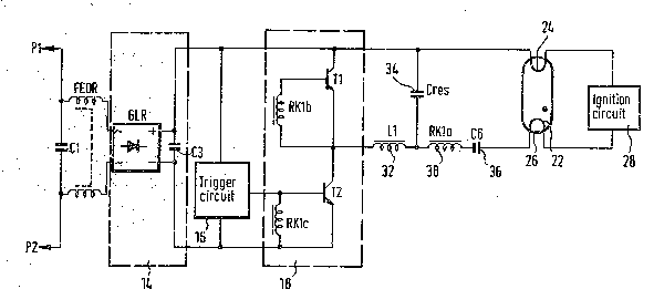
Fig. 5 corresponds to the embodiment of Fig. 4, whereby
a trigger circuit and a ignit;on circuit, described in
detail, are also indicated. The embodiment of the
trigger circuit corresponds to the cited
literature "Elektronikschaltungen" by W. Hirschmann on
pages 148 and 150 and the detailed embodiment of the
starter circuit corresponds to the disclosure of the
German patent specification 34 41 992.
: