Note: Descriptions are shown in the official language in which they were submitted.
~\
317 ~ 4 9 01KE88047
BAND REJECTION FILTERING ARRANGEMENT
:,,
BACKGROUND OF THE~INVENT_ION
This invention relates to filters and, more
, particularly, to an improved band rejection filter. Band rejection, or notch, filters are in g neral more
difficult and costly to implement~than bandpass filters,
which, for certain applications, have much less stringent
requirements. It is therefore an object of the present
invention to provide an arrangement which operates as a
band rejection filter but utilizes a bandpass filter.
Certain communications systems operate in a first mode
wherein all frequencies are passed and in a second mode
, wherein one or more frequency bands are rejected. It is
l therefore another object of this invention to provide an
! arrangement utilizing a bandpass filter in place of a
'-i; 15 notch filter which is selectively switchable to allow
l~l more than one mode of operation.
; ~ SUMMARY OF THE INVENTION
The foregoing, and additional, objects are attained in
accordance with the principles ~of this invention by
;~ providing a band rejection ~filtering arrangement which
comprises a quadrature~hybrid clrcult;having a first pair
of~ terminals and a second~pair o~ terminals, a first
bandpass filter~having its input~coupled to one of the
second pair of terminals~of~ the quadrature hybrid
25~ circuit,la first loadlcoupl~ed~to~the output of the first
?;~ bandpass filter, ~a second ~bandpass filter having its
nput coupled ~to the~other~of the second pair of
terminals of the~quadrature~hybrld cixcuit, a second load
,, . ; . , , . ,. . , ~ . - , .
,- ~
, ~ ' ,'' ' ~ ' '
,
31 7 6~9
coupled to the output of the second bandpass filter,
means for providing an input signal at a first of the
first pair of terminals of the quadrature hybrid circuit,
and means for receiving a signal at the other of the
first pair of terminals of the quadrature hybrid circuit.
In accordance with an aspect of this invention, the
first and second bandpass filters are ~uned to pass the
desired rejection band.
In accordance with a further aspect of this invention,
the arrangement further includes switching means for
selectively switching the arrangement between an all pass
mode and a band reiection mode. The switching means
comprises first controllable resistance means coupled to
the first of the second pair of terminals of the
quadrature hybrid circuit and the first bandpass filter
input, second controllable resistance means coupled to
the other of the second pair of terminals of the
quadrature hybrid circuit and the second bandpass filter
input, and control means coupled to the first and second
controllable resistance means for selectively causing the
first and second controllable resistance means to each
exhibit either a low resistance characteristic or a high
resistance characteristic in order to selectively achieve
; the all pass mode or the band rejection mode.
In accordance with yet another aspect of this
invention, the first and second controllable resistance
means each includes a PIN diode.
In accordance with still another aspect of this
invention, the control means includes means for
controlling the bias polarity of the PIN diodes.
BRIEF DESCRIPTION OF THE DRAWINGS
: The foregoing will be more readily apparent upon
; reading the following description in conjunction with the
drawings in which like elements in different figures
: 35 thereof have the same reference numeral and wherein:
FIG. 1 is a block diagram of a prior art switchable
.
~'.
1317~9
band rejection filtering arrangement;
FIG. 2 is a block diagram of a first embodiment of a
switchable band rejection filtering arrangement
constructed in accordance with the principles of this
invention; and
FIG. 3 is a block diagram of a second embodiment of a
switchable band rejection filtering arrangement
constructed in accordance with the principles of this
invention.
DETAILED DESCRIPTION
FIG. 1 illustrates a prior art approach to providing
a switchable band rejection filtering arrangement between
~; a transceiver 12 and an antenna 14. This arrangement
uses a notch filter 16 and PIN diodes 18, 20 and 22 as a
transfer switch. A PIN diode, illustratively of the type
manufactured by Unitrode Corporation of Lexington,
Massachusetts, is a semiconductor device that operates
as a variable resistor at radio frequencies and microwave
frequencies. The resistance value of the PIN diode is
determined only by its DC excitation. When a PIN diode
is forward biased, it exhibits a low resistance
characteristic. At high radio ~requencies, when a PIN
~ diode is at zero or reverse bias, it appears as a
;~ parallel plate capacitor with a parallel resistance which
is proportional to reverse voltage and inversely
proportional to frequency.
In the arrangement shown in FIG. 1, the PIN diodes 18,
20 and 22 are under the control of bias control circuit
24. The bias control circuit 24 i5 under the control of
the transceiver 12. When it is desired to operate the
system in an all pass mode, the transceiver 12 sends a
signal to the bias control circuit 24 to cause it to
forward bias the PIN diode 22 and to reverse bias the PIN
diodes 18 and~20. Accordingly, the notch filter 16 is
bypassed. Conversely, when it is desired to operate the
system in a band rejection mode, the transceiver sends a
' :~
~'
. ' .'', ~.: :,
. ' . .
13~7~49
signal to the bias control circuit 24 to cause it to
reverse bias the PIN diode 22 and to forward bias the PIN
diodes 18 and 20. This causes the notch filter 16 to be
inserted in the transmission path between the transceiver
12 and the antenna 14. Two major disadvantages of this
approach are that the full transmit power must pass
through the notch filter 16 and the PIN diodes and that
undesirably high insertion losses result.
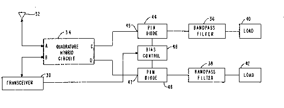
FIG. 2 illustrates a first embodiment of a system
constructed in accordance with the principles of this
invention which is an improvement over the prior art
system depicted in FIG. lo In the system shown in
FIG. 2, the transceiver 30 is coupled to the antenna 32
through the quadrature hybrid circ-lit 34. The quadrature
hybrid circuit 34, illustratively of the type
manufactured by Anzac Electronics of Waltham,
Massachusetts, is a low loss reciprocal four port device.
The relationship between signals at the ports A, B, C and
D is as follows. A signal appearing at the port A is
transmitted to the port C with some amount of attenuation
but no phase shift, and is transmitted to the port D with
some amount of attenuation and a 90 phase shift. A
signal appearing at the port B is transmitted to the port
D with some amount of attenuation and no phase shift, and
is transmitted to the port C with some amount of
attenuation and a 90 phase shift. A signal appearing at
the port C is transmitted to the port A with some
attenuation and no phase shift, and is transmitted to the
port B with some attenuation and a 90 phase shift.
signal appearing at the port D is transmitted to the port
B with some amount of attenuation and no phase shift, and
is transmitted to the port A with some amount of
attenuation and a 90 phase shift. There is isolation
between the ports A and B and there is isolation between
the ports C and D.
The band rejection mode of operation is achieved in
accordance with the principles of this invention by
, : .
'' .
` 131 7649
providing bandpass filters 36 and 38 terminated by
matched loads 40 and 42, respectively, all tuned to the
desired rejection band. Signals within the rejection
band are then absorbed by the bandpass filters 36, 38 and
the loads 40, 42, whereas signals outside the rejection
band are reflected by the out-of-band mismatch
characteristics of the bandpass filters 36, 38.
Switching between the all pass mode and the band
:`
rejection mode is accomplished by the PIN diodes 44 and
46, which are under the control of the bias control
;circuit 48, which in turn responds to signals from the
transceiver 30.
Typically, in the receive mode of operation, the
arrangement shown in FIG. 2 is operated as an all pass
network. In this mode of operation, the transceiver 30
~ provides a signal to the bias control circuit 48 to cause
;~it to reverse bias the PIN diodes 44 and 46 so that they
;act as high impedance devices. Accordingly, the signal
received by the antenna 32 enters the port A of the
20quadrature hybrid circuit 34 where it is divided by the
quadrature hybrid circuit 34 to the ports C and D. Due
to the high impedance mismatch of the PIN diodes 44 and
46, the divided signals are reflected back to the ports
C and D of the quadrature hybrid circuit 34, in which
25they are subsequently recombined at the port B and sent
to the transceiver 30.
In the transmit all pass mode, like in the
aforedescribed receive mode, the PIN diodes 44 and 46 are
reverse biased. Accordingly, the signal from the
30transceiver 30 which is applied to the port B of the
quadrature hybrid circuit 34 is divided to the ports C
and D. The divided signals a~re then reflected by the PIN
diodes 44 and 46 back to the~ports C and D, so that they
are recombined at the port A of the quadrature hybrid
~; 35circuit 34 for subsequent radiation from the antenna 32.
In the transmit band rejection mode of operation, the
PIN diodes 44 and 46 are forward biased so that they
,: :
-
,
13~76~9
exhibit a low impedance characteristic. The transmitsignal from the transceiver 30 is applied to the port B
o~ the quadrature hybrid circuit 34, which then divides
the signal and applies it to the ports C and D. Since
the PIN diodes 44 and 46 are forward biased to exhibit a
low impedance characteristic, the signals at the ports
C and D are applied to the bandpass filters 36 and 38,
respectively. The in-band characteristic of the bandpass
filters 36, 38 allows the in-band portions of the signals
to be passed therethrough to the loads 40, 42, where they
are dissipated. The out--of-band characteristic of the
bandpass filters 3~, 38 causes reflection of the
remaining portions (that which is wanted) of the transmit
energy back to the ports C and D. The wanted signals are
then recombined at the port A for application to the
antenna 32. It can be demonstrated that the ratio of
output power to input power at ports A and B is equal to
one quarter of the square of the sum of the reflection
coefficients at the points 45 and 47. If these
reflection coefficients are equal then the power ratio
equals the square of the reflection coefficient.
i The major advantage of the arrangement shown in
j PIG. 2 over that shown in FIG. 1 is that the PIN diodes
and the bandpass filters do not have to pass the full
power of the transmitted energy. Therefore, lower power
PIN diodes may be used, which results in lower insertion
losses. Also, the use of lower power PIN diodes greatly
reduces the generation of harmonics associated with high
- power PIN diodes. Additionally, bandpass filters can be
designed and built at lower cost and with less stringent
requirements than notch filters.
An alternate embodiment to the arrangement shown in
~` FIG. 2 is illustrated in FIG. 3. In this alternate
embodiment, the PIN diodes 44 and 46 are arranged in a
shunt, instead of a series, configuration. In the
embodiment illustxated in FIG. 3~ to achieve an all pass
mode of operation, the PIN diodes 44 and 46 are forward
/
,
1317~49
biased so that they are shorted to ground. The band
rejection mode is attained by reverse biasing the PIN
diodes 44 and 46 so they exhibit high impedance
characteristics.
Accordingly, there have been disclosed switchable band
rejection filtering arrangements. It is understood that
the abovQ-described embodiments are merely illustrative
of the application of the principles of this invention.
Numerous other arrangements may be devised by those
skilled in the art without departing from the spirit and
scope of this invention, as defined by the appended
claims.
,~
;
::;
. .
,
~ .
,