Note: Descriptions are shown in the official language in which they were submitted.
1317~5~
TEMPERATURE SENSING CIRCUIT
BACKGROUND
1. Field of the Invention
This invention relates to a temperature sensing
circuit and, more specifically, to a temperature sensing
circuit that provides an output relative to two temperature
transition points.
2. Description of Prior Art
Temperature sensing mechanisms are required in many
applications to determine temperature levels to insure proper
operation of equipment. Traditionally, temperature sensing
has been accomplished by mechanical devices that rely upon
mechanical changes of the device in response to temperature
changes of the mechanism. These mechanical devices often
develop reliability problems or vary from their designed
operational characteristics.
one object of the present invention i5 to provide a
reliable mechanism for sensing temperature.
SUMMARY OF THE INVENTION
In accordance with one aspect of the invention there is
provided a temperature sensing apparatus comprising: a first
and second set point temperature sensing circuit including a
thermistor for placement in operative association with a
medium and connected to a voltage divider having first and
second resistors of preselected values for generating first
and second voltages indicative of the medium's first and
second set point temperatures; and 555 timer having its
threshold and trigger inputs coupled to the voltage divider
for monitoring first and second voltages from the set point
temperature sensing circuit, said 555 timer outputting first
and second logic state output signals indicative,
respectively, of temperatures below the ~irst set point
temperatures and above the second set point temperature
~- wherein a hysteresis effect is generated for switching between
~: 35 the first and second logic state output signals.
,,"~.
;:
':~
.
. . . .
la ~ 7 ~ ~ 3
In accordance with another aspect of the invention there
is provided a method of monitoring the temperature of a medium
and generating a control output when the medium temperature
varies from a predetermined range defined by first and second
set point temperatures comprising the steps of: (a) sensing
the medium temperature using a temperature sensitive impedance
network having a sensor elsment in heat transfer relationship
with the medium for outputting medium temperature responsive
signals from said network; (b) coupling network output signals
to the trigger input of a 555 timer circuit so that when the
sensed medium temperature is altered in one sense direction to
one set point temperature the output state of the 555 timer
changes; (c) coupling network output signals to the threshold
input of said 555 timer circuit so that when the sensed medium 15 temperature is altered in the other sense direction to the
other set point temperature the output state of the 555 timer
changes again; and (d) coupling an output device to the 555
timer circuit output so that the timer output states provide a
control output for governing khe device in response to sense
medium temperature.
i..~
. . , ,~,
. . ~ . .
:. ' ' .
.
2 131 7~
In an embodiment of this invention, a temperature sensing
circuit is provided that includes a temperature sensing
element or thermistor with a resistance that varies according
to the temperature measured. An external resistor network is
connected to the thermistor. A circuit is connected to this
resistor network and the thermistor. The circuit includes two
comparators, a latch and an internal resistance network. The
external resistor network is connected to the comparators. An
internal resistor network i5 also connected to the
comparators. The circuit receives a voltage which is placed
across both resistive networks and sensing elements. The
voltage across the thermistor varies as a result of thermistor
resistance changes from temperatur~ variances. The
comparators compare the resulting voltages of the two
resistive networks and set or clear the latch accordingly.
The output of the latch is an output signal with two states.
The first state is provided when the element resistance
increases beyond a first transition point. The second state
is provided when the element resistance decreases beyond a
second transition point. The values of resistors in the first
resistor network are selected in combination with the
resistive range characteristics o~ the thermistor to provide
these transition points at preselected temperatures.
In a further embodiment of this invention, the output is
connected to a relay which may be used to activate a switch.
An application for this embodiment would be an air conditioner
; wherein the thermistor is placed on the evaporator coil and
the relay is connected to power the compressor. The
temperature sensing circuit would insure proper operation of
the compressor relative to the temperature condition of the
evaporator coil.
In a further embodiment, the temperature sensing circuit
may be self rontained within a housing providing a single unit
temperature probe.
~'
,...
. .
'
.
-3- t 3~7~3-,
BRIEF DESCRIPTION OF THE DRAWINGS
,
The above and other features and advantages of this
invention will become more apparent as the invention becomes
better understood by the detailed description that follows,
when considered in connection with the accompanying drawings.
FIGURE la is a schematic diagram of the temperature
sensing circuit invention.
FIGURE lb is a schematic diagram of a timer circuit.
FIGURE 2 is a schematic diagram of a second
embodiment of the temperature sensing circuit invention.
FIGURE 3 is a schematic diagram of a temperature
sensing circuit embodiment including a variable resistor for
adjusting a transition point.
FIGURE 4 is a pictorial view of a tempera-ture probe.
~ETAILED-DESCRIPTION OF ~HE PREFERR~D EMBOD~MæNT
This invention includes a temperature sensing circuit
with two temperature transition points. one transition point
provides an off-to-on output transition state and the second
transition point provides an on-to-off output transition state.
FIGURE la is a schematic diagram of an embodiment of
this invention. The device 20 is a 555 timer circuit and is
illustrated in FIGURE lb. Line 23 (FIGURE la) provides the
Vcc voltage input and a constant RESET-(i.e. reset always off)
to device 20. Line 21 is connected to ground. Line 18 is a
threshold and trigger input. Line 19 is a discharge line and
line 20 is a control voltage line. Line 22 is the output.
Device 20, the 555 timer, is detailed in the specification
information for the National Semiconductor LM555 contained in
the National Se~ic~r~ ol LlreaE ~ata~BGok-1983 and the
specification information for the~Intersil ICM 7555 contained
in the Intersil Data-Book.
... . . .. _
Capacitors 10, 14 and I7 are decoupling capacitors
~,
, :
' ' : ` ' `
,
,
i
_4_ 13~65~
that serve to ground any transient current components.
~esistors 11, 12 and 13 (Rll, R12, R13) are the source of
the input voltages for the circuit. Specifically, R12 is a
thermistor which is connected to the desired medium for
temperature measurement. Rll and R13 are fixed resistors.
In operation, the device 20 provides an output on line 22
which is directed through the coil 15 to trigger switch 16.
Coil 15 and switch 16 comprise a relay in the preferred
embodiment.
; 10 This embodiment is designed to measure a
temperature with R12 and provide an output signal on line 22
when the measured temperature rises above a first
temperature point and to terminate the output signal when
the measured temperature falls below a second temperature
point. Accordingly, Rll and R12 are selected to determine
the second temperature point and R13, in combination with
Rll and R12, select the first temperature point. In
operation, the resistive value of thermistor R12 increases
as the measured temperature becomes lower. Therefore, the
second or low temperature point is selected by having
Rll/ (R11 + R12) = 2/3, where R12 is the thermistor resistive
value at the low temperature point. The first temperature
point is selected by selecting R13 to satisfy the equation.
Rll R13
" R13 + R12
" Rll + R13 R12 = 1/3, where ~12 is the
: R13 + R12 thermistor resistive value
at the high temperature point
In this embodiment, the value of Rll may be selected
independently from the value R13.
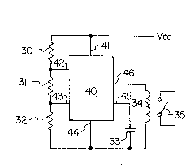
A second embodiment is illustrated in FIGURE 2.
Again, device 40 is a 555 timer circuit with line 41
connected to Vcc and line 44 connected to ground. Line 42
is the threshold input and line 43 is the trigger. Line 45
is the control voltage line and line 46 provides the output
signal to coil 34 which activates switch 35. The resistive
values of resistors 30 and 31 (R30 and R31) are selected to
set high and low temperature trigger points according to the
-, .
_5~
resistive/temperature characteristics of thermistor 32
(R32). For the low temperature trip point, the values of
R30 and R31 are selected to satisfy the equation:
R31_+ R32 = 2/3, where R32 iS the
R30 ~ R31 ~ R32 thermistor resistive value at
the low temperature point.
5 For the high temperature trip point, the valves of R30 and
R31 are selected to satisfy the equation:
R32 = 1~3, where R32 is the
R30 + R31 + R32 thermistor resistive value at
the high temperature point.
As an example of the embodiment in FIGURE 2, for a
thermistor with a resistive value of 30,000 ohms at 0C and
10 26,000 ohms at 3C, the values of R30 ànd R31 are 27,333
ohms and 24,667 ohms respectively. The resulting circuit
provides a temperature hysteresis between the transition of
0C and 3C. It should be apparent that a variable resistor
or potentiometer may be used to adjust the resistive values
15 to adjust the temperature trip points.
FIGURE 3 is an illustration of the invention with a
variable resistor. Device 80 is the 555 timer with lines 81
and 84 being Vcc and ground respectively. Lines 82 and 83
are the threshold and trigger lines with lines 85 and 86
being the output and control voltage lines. In this
embodiment, thermistor 53 is connected in parallel with
variable resistor 55 which provides an adjustment of the
thermistor resistive characteristics for a temperature
range. Additionally, R54 is provided~in addition to R51 and
R52 to provide trimming of the temperature difference
~between the high and low;temperature trip points. This
configuration results in a versatile ci~rcuit that may be
adjusted to yield the desired~ope~rating characteristics for
triggering switch 59~with coll 58.
~ The 555 timer ~is ~an~ integrated circuit that is
approximately equivalent to two comparators connected to a
flip-~lop or latch. The two comparators are connected to an
internal resistive network. It is the combination of the
;
: , ' , . '' ~ ;
--6--
values oE the internal resistive network together with the
external resistive networks that provide the operating
characteristics of the present invention. Thus, the proper
operation of the invention is independent of minor
variations in Vcc. Using a CMOS version of the 555 timer
5 will reduce the power requirements of the invention and
enable the sensing circuit to be used almost any place where
voltage is available for Vcc.
FIGURE 4 illustrates a still further embodiment,
wherein the invention is implemented as a temperature probe
10 having a thermistor 91 connected to a 555 integrated circuit
94 with two resistors 92 and 93 all mounted upon a board 97
and environmentally isolated by a case 96. The power and
output lines to and from the probe are provided on pins 95.
One application for this probe would be with an evaporator
15 coil of an air conditioner. The probe would be located
having the thermistor measure the evaporator coil
temperature. The output of the probe would activate a
switch which powers the compressor. When the temperature of
the evaporator coil falls below a low temperature trip point
the probe would deactivate the compressor. The compressor
would remain deactivated until the evaporator coil
temperature rises above a high temperature trip point
wherein the compressor would be reactivated. The output of
the invention would therefore be used to control the
compressor to ensure proper operation of the unit in
relation to the temperature of the evaporator coil.
Although the invention has been described in detail
in the embodiments within this specification, it is to be
understood by those familiar with the art, that this
invention may be embodied in other specific forms without
departing from the spirit or scope of the invention as
defined by the appended claims.
.,'~
'~
:
:
., .
.... . ~ .