Note: Descriptions are shown in the official language in which they were submitted.
1 31 8027
BACRGROUND OF THE INVENTION
The present invention relates to an encoder and a
decoder for residue number system data employed in a
digital signal processing circuit using residue operation.
Digital signal processing circuits such as a digital
filter and the like using residue operation have been
proposed. Refer to "IRE transactions on electronic
computers, Vol. EL-8, No. 6, June 1959, pp.l40-147",
"IEEE computer, Vol. 17, No. 5, May 1984, pp.50-61" and
"The transactions of the institute of electronics and
communication engineers, '84/4 Vol. J67-1, No. 4,
pp.536-543".
Since carry in operation becomes unnecessary in a
residue number system, operation of digital signals can be
carried out with high accuracy and high speed.
Then, after input binary data have been once converted
into a set of a plurality of residue data (hereinafter it is
called as RNS data), and desired operation has been carried
out in a residue number system, the obtained RNS data are
converted into output binary data once more.
In this time, if the conversion table is constituted
using ROM (Read Only Memory) in the encoder and the
decoder for the RNS data, the RNS data and the binary data
can be obtained with high speed.
However, in order to convert n-bit binary data into,
for example, RNS data represented by the plurality of Xi-bit
residue data, a ROM table having a capacity A represented by
1 31 8027
the following expression is needed with respect to each of
modula Mi (i = 0, 1, 2, ...)~
A = 2" . X; (bit).
For example, when the binary data and the residue data are
represented by 14 bits and 4 bits, respectively, the
capacity of the value represented by the following expression
is needed.
A = 214 x 4 = 65536 ~bit)-
There has been a problem that when a capacity of a
ROM table is made large in this way, the access time of the
ROM table is made so much the longer so that it is difficult
to convert binary data into RNS data.
Also, as a method by which RNS data are demodulated into
binary data, a Mixed Radix Conversion Method (hereinafter
called as MRC method) is known as shown in the paper entitled
"residue arithmetic and its application to computer
technology (1967)".
In this method, residue data composing RNS data are
applied with scale-down processing in order step by step
using a multiplicative inverse element of a value of one
modulus for that of the other modulus to reduce the number
of the residue data, and after residue data remaining
finally have been applied with processing of multiplication
using a fixed modulus, the RNS data are converted to binary
data by obtaining addition data.
In this case, however, since the residue data are
applied with scale-down processing in order step by step,
~'~'Y,~
3 ~ 3 1 8027
there is a problem that the whole configuration becomes
large-scaled.
Also, there has been another problem that though a
negative number can be represented by 2's complement binary
against natural or straight binary in binary data, a negative
number is not particularly defined in RNS data, and, therefor~,
processing of operation becomes complicated.
OBJECTS AND SUMMARY OF THE INVENTION
Accordingly, the object of the present invention is to
provide a new encoder and a new decoder for RNS data each of
which solves the conventional defects described previously.
In particular, the object of the present invention is to
provide an encoder and a decoder for RNS data, each of which
has a compact configuration on the whole and a rapid
conversion speed.
Another object of the present invention is to provide an
encoder and a decoder for RNS data which allow processing of
operation to be simplified by defining a positive number and
a negative number in RNS data.
BRIEF DESCRIPTION OF THE DRAWINGS
Fig. 1 is a rough sketch view showing the relation
between binary data and RNS data in an encoder and a decoder
according to the present invention;
Fig. 2 is a block diagram showing digital processing
devices such as digital filter and the like to which the
encoder and the decoder according to the present invention
are applied;
4 1 3 1 8027
Fig. 3 is a block diagram showing the principle of the
encoder for residue data according to the present invention;
Fig. 4 is a block diagram showing an embodiment of the
encoder for residue data according to the present invention;
Fig. 5 is a block diagram showing the principle of the
decoder for residue data according to the present invention;
Fig. 6A and Fig. 6B are block diagrams showing an
embodiment of the decoder for residue data according to the
present invention; and
Fig. 7 is a schematic diagram explanatory of the
operation of the decoder for residue data according to the
present invention.
DETAILED DESCRIPTION OF THE PREFERRED EMBODIMENT
At first, the relationship between binary data and RNS
data will be shown based on, for example, a Chinese remainder
theorem.
In other words, according to the Chinese remainder
theorem, if a remainder R~ of X with regard to the modulus
mi is represented by the following exp~ession (1) using a
mark MOD,
R~ = X MOD m~ ... (1).
RNS data DRo represented by the values Ro~ Rl, R2, ... Rj,
of remainder data pertaining to the modulus mO, ml, m2,
...m~, correspond to binary data having the value B
represented by the following expression (5) using the values
M, M~, and N~ which are represented by the following
relations ~2), (3), and (4), respectively.
,~ `,;
1 3 1 8027
M = ~ mi ... (2)
Nj = M/mj ... (3)
I = N~M~ MOD m; ... (4)
B = (~ R~M~Nj)MOD M ... (5)
In this case, the binary data and the RNS data have one-to-one
correspondence in the range which is not over the dynamic
range M of the RNS data.
If, in processing of operation of the residue data
composing the RNS data, the same procedure as in the case
where binary data are represented by 2' complement can be
employed for the processing of operation, the configuration
of the circuit for processing of operation can be made so
much the simpler.
As shown in Fig. 1, in general, n-bit straight binary
data can represent decimal digitslof 0 to 2n-1, and n-bit
binary data of 2' complement can represent decimal digits
of -2 to 2 1-1. On the other hand, RNS data can
represent decimal digits of 0 to M-l in total using a
dynamic range M shown by the expression (2). Then, the
region of the RNS data is assigned to regions of positive
numbers and negative numbers corresponding to 2's
complement binary data.
In the case where M is odd, the re~ion that the value
SRNs represented by the RNS:data is 0 to M-l represents
positive numbers and negative numbers are represented by the
region from the value M 1 + 1 to the value M-l.
, ~
6 ` 1 3 1 8027
The decimal digit 2n-1 represented by the straight
binary data is a decimal digit of -1 in the binary data of
2' complement. When this is represented by RNS data, it
becomes RNS data corresponding to complement representation
of M-l for a decimal digit M.
Since the expression 2n-1 + (M -2n) = M-l ... (11)
holds, when the value S of the straight binary data is in
the range of 0 ~ S ~ 2n 1_1, the residue data having the
value Ri represented by the following expression tl2)
constitute RNS data.
R~ = S MOD mi ... (12)
When the value S is in the range of 2n 1 ~ S ~ 2n-1, the
residue data having the value R~ represented by the expression
(13) constitute RNS data.
R~ = (S + M - 2n) MOD mi ... (13)
In other words, a positive or negative number is
distinguished by the most significant bit of binary data.
When the value of the most significant bit is zero (that is,
when it is a positive number), residue data of each modulus
mi are calculated from the binary data concerned. When the
value of the most significant bit is 1 (that is, it is a
negative number), after natural binary data are added with
the fixed value (that is, the value M - 2n) in such a
manner that the maximum value 2n 1 of the natural binary
data (that is, the value representedby binary data of 2's
complement -- 1) becomes the maximum value M - 1 of the
~NS data (that is, the value represented by the RNS data
~ ~ ",`,!
7 1 3 1 8027
--1), residue data of each modulus are calculated.
On the contrary, when RNS data are converted into
binary data of 2's complement, k-bit binary data capable of
representing the larger value than the dynamic range M of
the RNS data are made to correspond to the RNS data. When
the value SA of natural binary data decoded b~ the MRC
method is in the range of 0 ~ (M-1)/2, the value SA is judged
to be a positive number, and k-bit binary data of 2's
complement are obtained as they are. When the value SA is
in the range of (M-1)/2 + 1 ~ (M-l), the value SA is judged
to be a negative number, and binary data of 2's complement
are obtained by adding the value 2k -M to the value SA of
the natural binary data which have been decoded in such a
manner that the maximum value M-l of the value SA of the
binary data obtained by decoding the RNS data having the
dynamic range M becomes the maximum value 2k _ 1 of the
value SA of the k-bit binary data, that is, the value of
the k-bit binary data of 2's complement - 1.
Next, hereinafter embodiments of an encoder and a
decoder for RNS data according to the present invention
will be described in detail with reference to drawings.
At first, Fig. 2 shows a signal processing circuit
using residue operation. In Fig. 2, input binary data
~BI are supplied to an encoder 1 in which they are divided
by positive integers mO, ml, m2 ... mi having mutually
prime relation, and the residue data corresponding
respectively to the integers mO, ml, m2, m3 --, mi are
8 1 31 8027
output to a digital filter circuit 2 as RNS data DRI.
In the digital filter circuit 2, the plurality of digital
filt:ers corresponding to each figure of the RNS data DRI are
independently provided, operation of the RNS data DRI is
carried out for each figure under each modulus. Accordingly,
desired processing of operation for the binary data can be
executed with remarkably high speed compared with that in
direct processing of operation for the binary data.
The residue data output from the digital filters in the
digital filter circuit 2 are supplied to a decoder 3 as the
RNS data DRo and converted into output binary data DBo
therein.
Here, though the digital filter circuit 2 is composed
of the plurality of digital filters, one digital filter may
be employed in time sharing instead of the circuit 2.
Fig. 3 shows the principle of conversion of binary
data into RNS data in an encoder for residue data according
to the present invention, in which residue data Dj of the
modulus mi composing RNS data are obtained.
In other words, the n-bit straight binary data having
the value S are divided into the p-bit data Du having the
value Su (hereinafter it is called as the upper bit data)
and the q-bit data DL having the value SL (hereinafter it
is called as the lower bit data).
That is, the value S of the binary data can be
represented by the following relation (6).
S = Su x ~ ~ SL ... (6)
1 31 8027
The value R; of the residue data of the modulus m correspond-
ing to the value S concerned can be represented by the
following relation (7),
Rj = (SU X 2q + SL) MD mj
~ (SU X 2q) MOD m; + SL MD mj } MOD m; . . . (7)
In other words, a ROM table 10 receives the upper bit
data Du and outputs residue data DUI having the value RUj
represented by the relation (8) to a ROM table 12 via a latch
11 .
RU~ = (SU X 2P) MOD m~ ... (8).
On the other hand, a ROM table 13 receives lower bit
data DL and outputs residue data DLi having the value ~ i
represented by the relation (9) to a ROM table 12 via a
latch 14.
RL~ = SL MD m~ .., (9)
The ROM table 12 outputs the residue data D~ having
the value R~ represented by the following expression (10)
based on the residue data DU~ and DL~ as residue data of the
modulus mi composing the RNS data.
R~ = (RU~ + RL~) MOD m~ ... (10)
Accordingly, as shown by the expressions (8), (9), and
(10), the residue data Dj of the norm m~ can be obtained
from the added values of the residue data DUj of the modulus
mi obtained after giving weight of the value (that is, the
value 2q) corresponding to the upper bit data Du concerned
to the upper bit data Du and the residue data DL~ of the
modulus mi obtained from the lower bit data DLr thereby
;~
1318027
allowing the residue data Dj of the modulus m~ converted
into the RNS data from the binary data to be obtained.
At that time, if the value of the modulus mi is selected
in such a manner that the bit lenght Kj of the residue data
D~ becomes e~ual to r bit, in the ROM tables 10 and 13, the
capacities of the values represented by expressions
A1 = 2P x y and ~ z 2~ x y are needed, respectively. O~ the
other hand, in the ROM table 12 the capacity of the value
represented by the expression A3 = 22r x Y is needed.
Accordingly, a ROM table having capacity of Al + A2 ~ A3
= (2P ~ 2q + 22r) x y) in total is needed in order to obtain
the residue data D~ of the modulus m~.
However, for example, a ROM having the capacity of
65536 (bit) has been needed until now in the case where
four-bit residue data composing RNS data are obtained from
14 bit binary data. For this, the capacity needed can be
reduced to that of 3070 (bit), and the configuration of the
encoder circuit is formed so much the simpler on the whole,
allowing RNS data to be obtained with high speed.
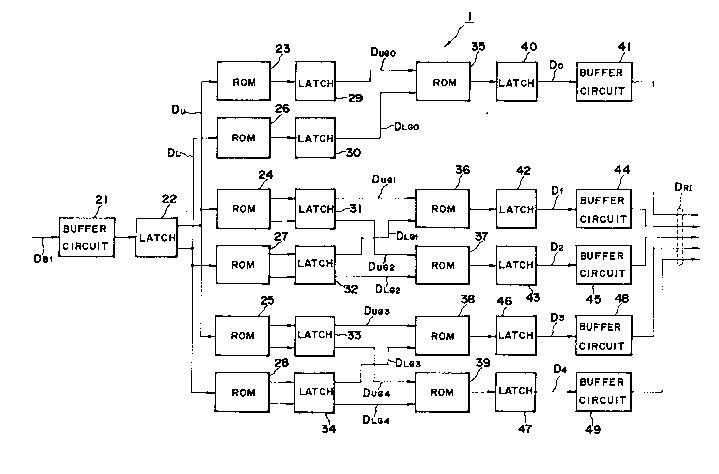
Next, a specific example of an encoder 1 will be
described. In Fig. 4, the encoder circuit 1 outputs RNS data
DRI composed of the residue data Do~D4 having the values 7,
11, 13, 15, and 16 of five modulus mO ~ m4~ from digital
image signal DBI, for example, composed of binary data.
In other words, in the encoder circuit 1, 14-bit binary
data rep~esented by 2's complement are received in a latch
22 via a buffer circuit 21 and separated into upper bit data
11 1318027
DU and lower bit data DL both comprising 7 bits, and t~le
separated data are supplied to ROMs 23, 24, and 25, and ROMs
26, 27, and 2~, respectively.
Thus, the buffer circuit 21 and the latch 22 divide
input data DBI comprising binary data for each desired bit
number, and, in this case, they form a data dividing means
which outputs a plurality of data comprising of upper bit data
and lower bit data.
The ROMs 26, 27, and 28 output residue data comprising
the lower bit data DL of the respecti~re modulus m0, that is,
its value is 7, ml and m2, that is their values are 11 and
13 respectively, and m3 and m4, that is, their values are
15 and 16 respectively. The ROMs 23, 24, and 25 output
~esidue data comprising the upper bit data Du of the respec-
tive modulus mO, ml and m2, and m3 and m4-
Thus, the residue data separated into the upper bitdata Du and the lower bit data DL are output, allowing the
capacity of the ROM tables needed for conversion of the RNS
data to be reduced on the whole, and an encoder having a fast
conversion speed with a simple configuration on the whole to
be obtained.
In the ROMs 24, 25, 27, and 28, one ROM is provided
with two conversion tables so as to output residue data of
modulus ml and m2, and residue data of modulus m3 and m4.
This is for effective utilization of the capacity of the ROM.
Accordingly, respective conversion tables may be provided in
independent ROMs.
! ~
12
1 31 8027
In the case where the residue data are separated into
the upper bit data Du and the lower bit data D~ and converted
by the ~OM, the value in the parenthesis of the expression
(13) can be rewritten into the following relation, that is,
S ~ M - 2n = (Su x 2q + Sl) + M - 2
= (Su x 2~ ~ M - 2 ) ~ SL
= (Su x 2q) ~ (M - 2n ~ SL) ... (14)
For example for the lower bit data DL, the ~esidue data
DLCi having the value F~ represented by the expression (9)
are output. On the contrary, for the upper bit data Du, the
region of positive numbers and that of negative numbers are
defined by ~he value Su of the data DU~ and when the value
Su i8 in the range of O < Su < 2~1-l, the residue data
DUG1 having the value Ru~ represented by the relation (15)
are output, and when the value Su is in the range of 2P-1 S
Su S 2P -1 the remainder data DLG~ having the value Ru~
represented by the relation (16) are output.
Ru~ = (Su x 2q) MOD mj ... (15)
Ru~ z (Su x 2q ~ M - 2n) MOD m~ ... (16)
Thus, the residue data having the value obtained by
adding the value of the residue data DUG~ to that of the
residue data DLG~ are obtained, and when positive and
negative numbers are represented correspondingly to positive
and negative numbers of binary data, RNS data can be obtained.
In the case where RNS data are converted using the way
of thinking described previously, after the
1 3 1 8027
above-mentioned 14-bit binary data are subjected to rounding to 13-bit binary data in
advance, the ROMS 26, 27 and 28 which receive the lower bit data DL are made to
output residue data having the value RLGj represented by the following expression
(17) in place of the residue data having the value represented by the expression (9).
RLGj = (SL + 1)/2 MOD In~ (17)
This means that lower bit data of 7 bits are subjected to rounding to 6-bit datain advance on the whole by adding the value 1 to the lowest bit of lower bit data DL
and then on~itting the lowest bit concerned, and the residue data DLG; are output with
respect to the rounded 6-bit data concerned.
On the other hand, the ROMS 23, 24, and 25 which receive the upper bit data
DU carry out processing of weighting of the value 26 corresponding to processing of
rounding the lower bit data DL to 6 bits, and output the residue data DUGj having the
value RUGj represented by the relation (18) when the value Su is in the range
represented by the relation 0 _ Su ~ 63 = 27~
RUGj = (SU X 26)MOD Inj ----- (18)
On the other hand, when the value Su of the upper bit data Du concerned is in the
range represented by the relation 64 < Su ~ 127 = 27-l. The residue data DUG
having the value RUGj represented by the relation (19) are output.
RUGj= (SU X 26 + M 213)MOD rnj ---(19)
1 31 8027
-14-
Here, the value M is represented by the following expression (20) from the
expression (2).
M = ~ m
i=0
= 7 x 11 x 13 x 15 x 16
=240240 ~-- (20)
Accordingly, since the residue data have been subjected to rounding to 13 bits,
they can represent the positive numbers from the value 0 to the value 8191 when the
value S of the whole of the binary data is in the range from the value 0 to the value
8191, and the negative numbers from the value -8191 to the value -1 when value S is
in the range from the value 8192 to the value 16383.
Accordingly, lLtce in this embodiment, even in the case where a digital video
signal SBI having the bit length of either of 13 bits and ?4 bits is input by receiving a
14-bit digital video signal SBI and processing of rounding it to 13 bits in advance, the
video signal SBI can be converted into RNS data v~lith practically sufficient accuracy.
Thus, the ROMs 23, 24, 25, 26, 27 and 28 give weight of the value 26 and the
value 2 to the upper bit data Du and the lower bit data DL~ respectively, and form a
first ROM table circuit for converting the upper and lower bit data Du and DL into
residue data DUGO, DUG1~ DUG2, DUG3~ DUG4, DLGO~ DLGI~ DLG2~ DLG3~ and DLG4 every
five norms mO ~ m4.
A ROM 35 receives, via latches 29 and 30, the residue data DUGO and DLGO of
the upper bit data Du and the lower bit data DL Of the modulus 7 which are output
-1S- 131802~
from the ROM 23 and the ROM 26 respectively and outputs, via a latch 40 and a
buffer circuit 41, the residue data DO having the value represented by the expression
(10) based on the residue data DUGO and DLGO concerned.
On the other hand, ROMs 36 and 37 receive, via latches 31 and 32, the
residue data DUGj and DLGj Of the upper bit data DU and the lower bit data DL Of the
modulus 11 and 13 which are output from the ROMs 24 and 27 respectively and
output, via latches 42 and 43 and buffer circuits 44 and 45, the residue data D1 and
D2 having the values represented by the expression (10) in the same way as the ROM
35.
ROMs 38 and 39 receive, via latches 33 and 34, the residue data DUG3 and
DLG3. and DUG4 and DLG4 Of the upper bit data DU and the lower bit data DL Of the
modulus 15 and 16 which are output from the ROMs 25 and 28 respectively and
output, via latches 46 and 47 and buffer circuits 48 and 49, the residue data D3 and
D4 having the values represented by the expression (10).
Thus, the residue data DO~ D4 of the modulus 7, 11, 13, 15 and 16 are
obtained via the buffer circuits 41, 44, 45, 48, and 49, and RNS data DRI comprising
the residue data DO, ~ D4 concerned can be obtained. Thus, the ROMs 35, 36, 37,
38, and 39 form a second ROM table circuit which converts the added values of the
residue data DUGO~ DLGO, DUG1, DLGI, DUG2, DLG2, DUG3, DLG3, DUG4, and DLO4 every
the modulus mO, m1, m2, m3, and m4 into the corresponding residue data DO, Dl, D2,
D3, and D4 of the norms mO, ml, m2, m3, and m4.
I 3 1 8027
-16-
With the above configuration, in obtaining the residue data based on the fixed
norms using the ROM table circuits, the residue data are separated into the upper bit
data and lower bit data and then processed, thereby allowing capacities of the ROM
table circuits to be reduced.
Accordingly, the configuration of the whole of the encoder circuit can be made
so much the simpler, allowing the conversion speed to be made high.
In the above-mentioned embodiment, the case where the lower bit data have
been subjected to processing of rounding has been described. But, the present
invention is not restricted to this case, but the processing of rounding has only to be
carried out as required.
Further, in the above-mentioned embodiment, the case where the 14-bit binary
data have been separated into the upper bit data of 7 bits and the lower bit data of 7
bits and then processed has been described. But, the bit length to be separated is not
restricted to 7 bits, for example, the binary data may be separated into data of 6 bits
and 8 bits, and the bit value can be selected to a desired value as required.
Further, in the above-mentioned embodiment, the case where the binary data
are separated into two kinds of data, that is, the upper bit data and lower bit data for
processing has been described. But, the present invention is not restricted to this, for
example, the binary data may be separated into three kinds of data, or the binary
data may be separated into plural kinds of data for processing as required.
Next, the decoder 3 will be described. The decoder 3 receives RNS data DRO
output from the digital filter circuit 2 and outputs binary data D,30, based on, for
example, such the MRC method as described previously.
1318027
-17-
The MRC method will be described more in detaiL At first, with respect to
the residue R; of S pertaining to the modulus m; shown in the expression ~1),
assuming that S is generally represented by X, the value X; represented by the
follovwing expression (21) is defined to be a multiplicative inverse element of X
pertaining to the modulus m.
1 = (Xj.X) MOD m; (21)
provided that 0 s X < mi
Then, the value Rïï is obtained, which satisfies the expression (22) representedusing the values R; and Rj of the residue data pertaining to the moduli mj and mj and
the multiplicative inverse element Xj of the value mj pertaining to the modulus m;.
Rj; = ~(R; - Rj)Xj} MOD m; (22)
This processing is called as a scale-down processing pertaining to the modulus mj in
the present specification.
The scale-down processing is parallelly repeated in sequence for
predetermined residue data to gradually reduce the number of residue data which
require the scale-down processing and obtain a plurality of residue data
corresponding to the modulus of the ~S data. After the residue data are
multiplicatively processed using a predetermined modulus, added data are obtained,
thereby converting the RNS data into binary data
The fundamental principle of the decoder will be explained using Fig. 5.
Residue data Do~ Dl, and D2 pertaining to the moduli m~, ml, and m2, among RNS
h''
1 31 8027
-18-
data consisting of residue data Do~ Dl, D2, and D3 pertaining to the moduli mO, ml,
m2, and m3 which are provided via latch circuits 50, 51, 52, and 53 are supplied to
ROM table circuits 54, 55, and 56.
Furthermore, ROM table circuits 54, 55, and 56 receive residue data D3
pertaining to the modulus m3 via the latch circuit 53.
The ROM table circuit 54 outputs residue data Dlo having the value Rlo based
on the expression (22) using a multiplicative inverse element X03 Of the value m3 (that
is, the modulus of the residue data D3) pertaining to the modulus m~, with the values
of the residue data Do and D3 set at Ro and R3. The ROM table circuit SS outputsresidue data Dll having the value Rll based on the expression (22) usmg a
multiplicative inverse element Xl3 of the value m3 pertaining to the modulus m; with
the value of the residue data Dl set at R~. The ROM table circuit 56 outputs residue
data Dl2 having the value Rl2 based on the expression (22) using a multiplicative
inverse element X23 of the value m3 pertaining to the modulus m2 with the value of
the residue data D2 set at R2-
The outputs of the ROM table circuits 54, SS, and 56 and the latch circuit 53are again provided to ROM table circuits 61, 62, and 63 via latch circuits 57, 58, S9,
and 60. The ROM table circuit 61 receives the residue data Dlo and Dl2 and outputs
residue data D20 having the value R20 based on the expression (22) using a
multiplicative inverse element X02 of the value m2 pertaining to the modulus mO.
I 3 1 ~027
-19-
The ROM table circuit 62 outputs receives the residue data Dll and D,2 and
outputs residue data D2, having the value R21 based on the expression (22) using a
multiplicative inverse element Xl2 of the value m2 pertaining to the modulus ml.On the other hand, the ROM table circuit 63 receives the residue data D3 and
Dl2 and outputs addition data DA1 of the value SA1 represented by the following
expression (23).
SAI = Rl2.m3 + R3 ------------- (23)
The outputs of the ROM table circuits 61 and 62 are supplied to a ROM table
circuit 66 via latch circuits 64 and 65.
The ROM table circuit 66 receives the residue data D20 and D21 and outputs
addition data DA2 Of the value SA2 represented by the following expression (24). SA2 = ~20.ml.m2.m3 + R2l.m2.m3--- (24)
The outputs of the ROM table circuits 63 and 66 are provided to an addition
circuit 70 via latch circuits 67, 68, and 69 to obtain output data represented by a
binary code of the value SA represented by the following relation (25).
SA = SA1 + SA2 = R20.m1.m2.m3 + R2~.m2.m3
+ R2l.m3 + R3 ------ (25)
In other words, RNS data DRO consisting of the residue data DO ~ D3 of the
moduli mO ~ m3 are converted into binary data DBO-
Next, the pnnciple of the embodiment of the decoder circuit according to thepresent invention vrill be explained. In the present invention, the modulus of the
value of the power of 2, that is, 2' is applied to the modulus of residue data which are
1 31 8027
-20-
firstly scale-down processed. Thus, if addition data of the value SB represented by the
following relation (26) is made to output f~om the expression (25), the RNS data DRO
can be demodulated into the binary data DBO-
SB = R20-m1-m2-2~ + R21.m2-2~ + Rl2-2~ + R3 ------(26)
This means that the values ml.m2.m3, m2.m3, and m3 are not be
multiplicatively processed for the values R20, R2l, and Rl2 of the residue data D20, D2l,
and Dl2 respectively in the first, second and third terms of the right side of the
expression (26), but even if bit shift is carried out by the value Q of the exponential
part of the modulus m3 represented by a power of 2 to add it to the residue data R3
after the values ml. m2, m2, and 1 are multiplicatively processed, the RNS data can be
demodulated. This also means that operation processing works in demodulating theRNS data can be simplified so much.
Concretely, the ROM table circuit 66 outputs addition data DR2 rep~esented by
the relation (27) to an adder 70.
SB2 = R20.ml.m2 + R2l.m2 -------- (27)
Furthermore, the ROM table circuit 63 is omitted and made to output residue
data D3 and Dl2 directly to the adder 70 via a predetermined latch circuit (not
shown).
In the adder 70, the addition data DR2 and the residue data D,2 are bit-shifted
by Q bits toward the higher order bit side, and the residue data D3 and Dl2 are added
with the addition data DR2 respectively to output them.
1 3 1 8027
-21-
Accordingly, addidon data having the value SR represented by the following
relation (28) can be obtained via the adder 70. It is found that substituting the
expression (27) into the expression (28), binary data DBO demodulated based on the
MRC rnethod can be obtained.
SB = SR2.2 + Rl2.2 + R3---- (28)
Thus, by having selected the modulus m3 which firstly carries out scale-down
processing to the value 2~ represented by a power of 2, the ROM table circuit 63which outputs residue data represented by the third term of the right side of the
expression ~26) can be omitted.
Moreover, in the ROM table circuit 30, though the modulus m3 has to be
multiplicatively processed corresponding to the first and second terms of the right side
of the expression (25), it is sufficient to output residue data which are multiplicatively
processed with respect to the moduli ml.m2 and m2 correspondingly to the expression
(26). The ROM table circuit 30 can be configurated the simpler.
Now, some decoder circuits of this kind are provided with function of the so-
called round processing by which after a predetermined bit in addition data is added
with the value 1 in outputting binary data, bits below the addition bit concerned are
cut off for outputting
But, in order that the addition data obtained in this way is applied with round
processing to output thereof after adding the value 1 directly to the predetermined bit
therein, an extra adder having the same bit length as the adder æ has to be provided,
and there is a problem that the configuration of the whole of the decoder circuit
becomes the more complicated.
~t
~ 3~ 8027
æ
Then, an adder 71 of, for example, 8 bits is provided between latches 67 and
69, and the value 1 is added to the predetermined bit in the addition data DBO by
adding the round processed data D3 to the data before the addition data DBO are
obta~ed (in this case, the addition data DA1) instead of the addition data DBO
When, for example, 7, 11, 13, and 15 are selected as the moduli m~p ml, m2,
and m3, the maximum value SA1 MAX of the addition data DA1 input to the adder 71
can be represented by the following relation (29) from the expression (æ).
SA1 MAX < 12 x 15 ~ 14 ~ 194 (29)
In other words, data having the maximum value 194 are obtained in the
addition data DA1~ which can be represented by the length of 8 bits. Even if the value
61 represented by the following expression (30) is added to the ma~nmurn value, it is
found that carry which exceeds the most significant bit does not yield.
(28- 1)- 194 = 61 --------- (30)
Accordingly, the following relation (31) can be obtained with respect to the
value 61.
2 > 61 > 2 ---------- (31)
If the value 1 is added in the adder 71 concerned in the range up to the fifth bit
counted from the least significant bit represented by 25, it is found that the bit length
does not vary in the addition data output from the adder 71.
Accordingly, if the value 1 is added in the range up to the fifth bit counted
from the least significant bit in the adder 71, the same result of addition as that in the
1 31 8027
-23-
case where the value 1 is added in the range up to the fifth bit counted from the least
significant bit can be obtained in the addition data DBO output from the adder 70
using the adder 70 as it is without replacing its configuration~
For this, since the least common multiple M of the moduli m~ ~ m3 are
represented by the following expression (32), the data having the ma~mum value of
15014 (that is, the value M-l) can be obtained.
M = m~,~m,.m2.m3 = 15015 -----(32)
Accordingly, when the data having the value 15014 are represented by binary
data, the relation represented by the following expression (33) is solved to obtain the
value n = 14, from which it is found that the binary data are represented by the data
having the length of 14 bits.
2n- 1 > 15014 ~ 2n-1 - 1 ---- (33)
Accordingly, in the case where the addition data DBO are applied with round
processing after the value 1 is added to the predetermined bit therein, an extra 14-bit
adder is needed.
Thus, in the case where the addition data DBO are directly round-processed, a
14-bit adder is required for the round processing~ For this, by adding the value 1 to
the above predetermined bit in the range up to the fifth bit counted from the least
significant bit using the adder concerned 71, the preparation of the 8-bit adder 71
allows addition data DBO added with the value 1 to the desired bit therein to be
obtained and the whole configuration to be simplified so much~
1 31 8027
-24-
Next, a concrete embodiment of a decoder circuit according to the present
invention applied with this fundamental principle will be described using Figs. 6A and
6B.
The decoder circuit 3 consists of the data conversion circuit part 100 shown in
Fig. 6A and the latter half part 150 shown in Fig. 6B.
The RNS data DRO represented using the moduli m~, ml, m2, and m3 of the
values 7, 11, 13, and 15 and the modulus m4 of the value 16 the value of the power of
2 are employed here.
In other words, in the data conversion circuit part 100, the residue data Do~ Dl,
D2, D3, and D4 (that is, corresponding to the moduli m0, ml, m2, m3, and m4) which
compose the RNS data DRO are input to latches 106, 107, 108, 109, and 110 via buffer
circuits 101, 102, 103,104, and 105, respectively.
ROM table circuits 111, 112, 113, and 114 receive residue data D4 of the
modulus m4 of the value 16 in addition to the residue data Do~ Dl, D2, and D3 and
output residue data Dlo, Dll, Dl2, and Dl3 of the moduli m0, ml, m2, and m3,
respectively.
In other words, with multiplicative inverse elements of the value 16 (that is,
pertaining to the modulus m4) pertaining to the moduli m0, ml, m2, and m3 of values
7, 11, 13, and 15 respectively set to values X~4, X14, X24, and X34, respectively, residue
data Dlo, Dll, Dl2, and Dl3 having values Rlo, R~l, Rl2, and Rl3 represented by the
following expressions (34), (35), (36), and (37) respectively are output and scale-down
processed with respect to the modulus m4 of the value 16 represented by a power of
2.
., .., ,~
rr~
1 31 ~02~
Rlo = ~(Ro - R4).X04} MOD mO (34)
Rll = {(Rl - R4).Xl4} MOD ml (35)
Rl2 = {(R2 - R4).X24} MOD m2 (36)
Rl3 = {(R3 - R4).X34} MOD m3 (37)
ROM table circuits 119, 120, and 121 receive the residue data Dlo, Dll, and
D,2 via latches 115, 116, and 117 respectively, and at the same time, receive the
residue data Dl3 via a latch circuit 118, then they output residue data D20, D2l, and
Dæ Of the moduli m0, ml, and m2.
In other words, with multiplicative inverse elements of the value 15 (that is,
the modulus) pertaining to the moduli m~, ml, and m2 of values 7, 11, and 13 set to
values X03, Xl3, and X23 respectively residue data D20, D2l, and Dæ having values R20,
R2l, Ræ represented by the following expressions (38), (39), and (40) respectively are
output and scale-down processed with respect to the modulus m3.
R20 = {(R1o - Rl3).X03} MOD mO -- (38)
R2l = {(~ll - Rl3).Xl3} MOD ml --- (39)
R22 = {(Rl2 - Rl3).X23} MOD m2 ~~- (40)
Furthermore, ROM table circuits 125 and 126 receive residue data D20 and D
via latches 122 and 123 respectively, and at the same time, residue data Dæ via a
latch 124, and output residue data D30 and D3l of the moduli m~ and ml.
In other words, with multiplicative inverse elements of the value 13 (that is,
the modulus m2) pertaining to the moduli mO and ml of the values 7 and 11 set to
1 3 1 8027
-26-
values X02 and Xl2, residue data D30 and D3l having values R30 and R3l represented
by the following expressions (41) and (42) are output and scale-down processed with
respect to the modulus m2.
R30 = ~(R20- R22).X02} MOD m0-- (41)
R31 = ~(R21 - R22)-XI2} MOD ml___ (42)
ROM table circuits 129 and 130 receive the residue data D30 and D3l
concerned via latches 127 and 128, and output addition data DA3U and DA3L which are
higher order 6 bits and lower order 8 bits of the addition data DA3 having the value
SA3 represented by the following expression (43) to latches 131 and 132 respectively.
SA3 = R30-ml-m2-m3 + R31-m2-m3
= R30-11-13-15 + R3l.13.15 --(43)
For this, ROM table circuits 134 and 135 receive residue data D22 and D13 via
latches 124 and 133, and output addi~ion data DA4U and DA4L which are higher order
4 bits and lower order 4 bits of addition data DA4 having the value SA4 represented by
the following expression (44) to an adder 138 via latches 136 and 137.
SA4 = R22-m3 + Rl3 = R22.15 + Rl3 (44)
On the other hand, a buffer circuit 139 is supplied with a control signal Dc of
two bits for round processing. A decoder 140 selectively outputs the value of addition
data Dc of three bits in accordance with the value of the above control signal and
supplies it to the adder 138 via inverted amplifier circuits 141, 142, and 143.
The adder 138 receives the addition data DC concerned, which is added with
~1$~,
-27-
addition dah DA4U and DA4L output from the ROM table circuits 134 and 135, both
being bit-shifted by three bits from their least significant bit. The output of the adder
138 is output to latch circuits 144 and 145.
~ inally, in an adder 146, when the value of the addition data Da output from
the decoder circuit 140 is 0, the result of addition of the value SA represented by the
following relation (45) can be obtained from the expressions (43) and (44).
SA = R30 ml.m2.m3 + R31.m2.m3 + R22-m3 + R13
= R30.11.13.15 + R3l.13.15 + Ræ.15 + Rl3 (45)
Accordingly, when the above result of addition is subjected to operation
processing so as to be represented by the following relation (46), the RNS data DRO
can be demodulated into binary data having the value SA.
SA Z SA m4 + R4
= (R30 11.13.15 + R3l.13.15 + R~.15
+ Rl3).16 + R4
= R30.11.13.15.16 + R3l.13.15.16
+ R22.15.16 + R,3.16 + R4-~ (46)
A,ccordingly, in this case, if the result of addition SA is added with residue data
D4 having the value R4 after it is bit-shifted by four bits correspondingly to the value
4 of the exponential part of the module represented by a power of 2, addition data
represented by the MRC method can be obtained.
In other words, in addition data obtained from the RNS data represented by
the moduli mO ~ m4 using the MRC method, since the least common multiple of the
moduli mO ~ rn4 are represented by the following expression (47), the following
1 3 1 8027
relation (48) is solved to obtain the value n = 18. The RNS data DRO can be
represented by binaty data of 18 bits as a whole.
M = ~ mi = 7.11.13.15.16 = 240240 ~(47)
i=O
2~' - 1 s 240239 s 2-q -1 -~--- (48)
The addition data DA Of 14 bits are output by omitting four bits of the additiondata in advance.
In other words, when the addition data represented by the exptession (46) are
subjected to processing of scaling to omit four bits, processing of scaling of dividing by
the value 16 can be executed by o~y adding addition data DA3U~ DA3L' DA4U~ and
DA4L as they are, which are output from ROM table circuits 129, 139, 134, and 135
and represented by the expression (45).
Thus, the modulus m4 is set to the value 16, and at the same time, scale-down
processing is firstly applied to the modulus m4 concerned, thereby allowing the
configuration of an adder in processing of scaling to be simplihed, and the whole of
the configuration of the decoder 3 to be simplified so much.
On the other hand, the decoder circuit 140 is designed in such a manner that
the values of the addition data Da are sequentially changed-over between the values
r1, Q OJ,rO, 1, OJ, and rO, O, 1J in order from the most significant bit for outputting
them, and the value 1 is added to the fifth bit, fourth bit, and third bit counted from
the least significant bit as a whole by shifting the addition data DC1 concerned by
three bits and adding them to the addition data DA.
Furthermore, the decoder circuit 140 is so designed that the value of the
addition data DC can be changed over to the value rO, O, OJ and the addition data DA
not subjected to round processing can be selected.
This embodiment is so designed that since the addition data DA Of 14 bits are
output as they are without omitting bits below the bit added with the value 1, bits up
to the necessary bit ~om the most significant bit can be selectively employed inaccordance with the bit added with the value 1.
1 3 1 80~7
-29-
Now, in the case where negative numbers are dealt with in tbe decoder circuit
3, the cliscrimination between positive numbers and negative numbers has to be done
by the judgement whether the value of demodulated natural binary addition data is
larger than the fixed value (in this case, the value (M-1)/2 + 1)) or not. For the
judgement in practice, a comparator circuit having large bit numbers is needed, which
brings up a problem that the configuration of the whole of the decoder circuit is
complicated so much, and the configuration of the whole of the signal processingcircuit becomes complicated as well.
Then, in the decoder circuit 3 according to the present invention, the addition
data DA output from the data conversion circuit part 100 are added with the fixed
value, and positive numbers are discriminated from negative numbers by the most
significant bit of the added value obtained.
In other words, as shown in Fig. 6B, in the circuit part 150 in the following
stage which receives the addition data DA from the data conversion circuit part 100,
an adder 151 receives the higher order 12 bits of the addition data DA via a latch
circuit 152, and at the same time, receives addition data DC2 having the value 171
output from an addition data generating circuit 153. Data of the most significant bit
of the result of addition are sent as a discriminating signal Dj.
This will be described using Fig. 7. Since the addition data DA obtained by
demodulating RNS data are addition data of which higher order 14 bits are subjected
to processing of scaling, the addition data represent negative numbers when the
addition value SA is between (Ml6 - 1)/2 + 1 and (M16 - 1). In this case, the value
Ml6 is 15015 of 1/16 times the minimum common multiple M = 240240 of the
moduli m4 ~ m4 since the addition data DA are subjected to processing of scaling by
four bits. On the other hand, in the k-bit binary data, negative numbers are
represented when the value S at which the most significant bit is given the value 1 is
between 2k and 2k-1.
Accordingly, if the addition data DA are added with the fixed value in such a
manner that the minimum value which represents negative numbers of the addition
data DA concerned, that is, (Ml6 -1)/2 + 1 becomes the minimum value of the bina~y
data concerned which represent negative numbers (that is, the value 2k-'- 1), and the
1 3 1 8027
-3~
addition data D~,~ are converted into the fixed data (hereinafter called as conversion
data), in the value STR Of the conversion data concerned, the value of the most
significant bit is changed over from 0 to 1 in the case where the value of the addition
data DA represents negative numbers.
If the operation is done in this way, it is possible to discriminate positive
numbers from negative numbers using a only simple configuration by which the
addition data DA are added with the fixed value without comparing all of 14 bits to
output the most significant bit allowing the decoder cIrcuit 3 having a simple
configuration as a whole to be obtained.
In the case wbere the discrimination is carried out using higher order 12 bits, it
is sufficient to add the value 171, that is, the value obtained by dividing 685 by 2 by
cutting two bits, while it is essentially necessary to add 684 up to 14 bits. This
reduces size of hardware.
An adder 154 receives the addition data DA via a latch circuit 155. The
addition data DA concerned are added ~,vith addition data D~3 output from an addition
data generating circuit 156, and the added data are output from the adder 154. In
other words, the adder 154 receives via an AND circuit 159 a bipolar switching signal
D~ obtained via a buffer circuit 157 together with a discriminating signal Dj
obtained from the adder 151 via a latch circuit 158 and adds to the addition data DA
the value 1369 (that is, 2~' - Ml6) which is output from the addition data generating
circuit 156 at the timing when the logic level of the discriminating signal D3 rises to
logic rl, and output the added data.
AS a result, in the adder circuit 154, when the addition data DA represent
negative numbers, binary data added with the value 1369 are obtained for the
addition data DA. On the contrary, when the addition data DA represent positive
numbers, the addition data DA are output as they are.
Thus, the addition data DA are converted into binary data of 2's complement,
which can be output.
For this, the adder 154 outputs the addition data DA irrespective of the logic
level ~ the discriminating signal Dj as they are when the bipolar switching signal
DBIUN is changed over.
-31- t 31 8027
As a result, the adder 154 allows bipolar binary data to be switehed and output
as required by switching the bipolar switching signal D~
The adder 154 outputs higher order 13 bits among the binary data concerned
having 14 bits via a latch circuit 160 and a buffer circuit 161, and at the same time,
outputs the most significant bit of the binaTy data concemed via an inverted amplifier
163, a latch circuit 164, and a buffer circuit 165, thereby outputting binary data D~oo
comprising bipolar binary data and offset binary data
When a fixed bit of data having a short bit length before the addition data DA
are obtained is added with the value 1, the addition data DA having a large value as a
whole are obtained in accordance with the addition bit concerned, and sometimes it is
judged by mistake that the addition data DA representing the larger value of a
positive number represent negative number.
In other words, in the case where the value 1 is added to, for example, the
(y+ 1) bit counted from the most significant bit to apply processing of rounding to L
bits to the addition data DA. the addition data DA are represented by the data of the
value added with the value 2~fl to the whole of the addition data because the (y +
1) the bit is added with the value 1. Thus, the maximum value and the minimum
value change from the value (M-1)/2 and (M-1)/2 + 1 to (M-1)/2 + 2~'-Y I and (M-1)/2 +1 + 21'-Y-l, respectively.
Accordingly, when the addition data have a larger value than the value (M-
1)/2 + 1 +2~'-Y I, the value of the addition data Da from the addition data generating
circuit 153 is set so as to allow the region representing negative numbers to bediscriminated, and at the same time, if the value of the addition data from the
addition data generating circuit 156 is set to the value (2~ - M-2~-Y-1) in such a manner
that the maximum value (M - 1 + 2~'-Y l) of the addition data DA becomes the value
(21'-1-2~-Y-I) smaller than the maximum value (2" - 1) of the binary data D~O by the
value 2~-Y-I (that is, the addition data DA is assigned to the region having a smaller
value of a negative number than the regular value by the value increased as a whole),
bipolar binary data obtained by adding the value 1 to (y + 1) the bit counted from
the most significant bit can be obtained.
1 3 1 ~027
-32~
Variations described below are considered in the encoder described above.
When positive and negative numbers are assigned to regions represented by
RNS data in the above-mentioned embodiment, the case where the fixed value (thatis, the value (M - 2n)) is added to data of higher order bits is described. The method
by which positive and negative numbers are assigned is not restricted to the above
method. For example, there are the case where after the fixed value (M - 2n) is
added to data of lower order bits, residue data are obtained from the result of
addition concerned and the case where the value (M - 2n) is added to the added value
of the residue data which are obtained from data of higher order bits and data of
lower order bits. This method is widely applicable to these cases and the like.
Further, in the above-mentioned embodiment, there has been described the
case where unipolar binary data obtained by the MRC method are converted into
bipolar binary data. But, the means by which RNS data are converted is not
restricted to this. For example, the residue theorem by a Chinese and the like can be
widely applicable.
Further, in the above-mentioned embodiment, there has been described the
case where RNS data are subjected to processing of scaling in converting thereof into
binary data and at the same time, subjected to processing of rounding. The present
invention is not restricted to this case, but RNS data may be subjected to processing
of scaling or rounding as required.
Further, in the above-mentioned embodiment, there has been described the
case where addition data are converted into bipolar binary data to output them. The
present invention is not restricted to this case, but RNS data may be, for example,
directly output as required.
Further, in the above-mentioned embodiment, there has been described the
case where the fixed bit of the addition data DA4 output from the ROM table circuits
134 and 135 is added with the value 1. The present invention is not restricted to this
case, but, for example, the fixed bit of the residue data Dl3 may be added with the
value 1.
Further, in the above-mentioned embodiment, there has been described the
,,~3 ~p
1 3 1 802~
-33-
case where the fixed bit is added with the value 1 in such a manner that bits do not
overflow in the adder 138. The present invention is not restricted to this case, but
bits are made to overflow as required, and addition data having a so long bit length
may be output to the adder 146. Even if the addition data are output like this,
processing of addition may be applied to addition data having the bit length of eight
bits compared with the case where processing of addition is applied to addition data
having the bit length of 14 bits, thereby allowing the whole configuration to besimplified so much.
Further, in the above-mentioned embodiment, there has been described the
case where binary data of 13 bits are output by obtaining addition data of 14 bits of
which fixed bit is added with the value 1. The bit length which is output is notrestricted to this, but the length of the bit which is output as required may beswitched in accordance with the bit added with the value 1.
Further, in the above-mentioned embodiment, there has been described the
case where negative numbers are detected by adding the value 171 to the data of the
higher order 12 bits of the unipolar binary data of 14 bits. The present invention is
not restricted to this, but negative numbers may be detected by adding the value 684
to bina~y data of 14 bits, the bit length is selected within a sufficient tange in
practical application, and at the same time, the added value may be set in accordance
with the above bit length.
Further, in the above-mentioned embodiment, there has been described the
case where unipolar binary data having the region of the value 15015 represented by
an odd number of 1/16 times the minimum common multiple of the moduli mO ~ m4
to which positive and negative numbers are assigned and converted into bipolar
binary data by the application of processing of scaling thereto. But, in the case where
the region concerned is represented by an even number, the value (2k - M)/2 is
added in place of the value (2k - M - 1)/2, and the most significant bit of the result of
addition may be used as a discriminating signal Dj.
Further, in the above-mentioned embodiment, there has been described the
1 31 8~27
-34-
case where RNS data are obtained with respect to five moduli of the values 7, 11, 13,
15, and 16. lhe number and the value of the moduli are not restricted to this, and
they c~m be selected to various values as required.
Further, in the above-mentioned embodiment, there has been described the
case where digital video signals composed of binary data of 14 bits are converted into
RNS data. The bit length of binary data is not restricted to this, but that in the wide
range is applicable.
Further, in the above-mentioned embodiment, there has been described the
case where the present invention is applied to encoder circuits and decoder circuits in
digital filter circuits. The present invention is not restricted to this, but is widely
applicable to digital signal processing circuits for audio signals, video signals, and the
like.