Note: Descriptions are shown in the official language in which they were submitted.
~3~3~7
The present invention relates to a signal processing
unit for use in electronic equipment and, specifically,
relates to a signal processing unit for use in a radio
telecommunication apparatus such as a pager, a cordless
telephone, or a mobile telephone.
In recent years, a new type of paging system has been
developed in which a base station transmits message
information, and any called one of the pager receivers
1~ subscribed to this system displays the mess~ge information.
The paging signal used in this system is formed as follows.
Each frame of the paging signal is time-divided into n
groups. Further, each group is time-divided into one
synchronization on preamble word and m calling words. Each
calling word is formed of an identification (ID) code and a
message code.
To call a selected pager receiver, a caller dials a
telephone numbers assigned to the pager receiver, thus
reaching the base station. Then, the caller sends message
information to the base station. The base station generates
the ID code assigned to the selected pager receiver and the
message code corresponding to the message information, and
inserts these codes into one of vacant calling words of that
group of the paging signal to which the selected pager
receiver belongs. Then, the base station transmits the
paging signal.
~3~3~S7
Each pager receiver comprises an antenna, a receiver
circuit, a control circuit, and ID ROM, a drive circuit, a
loudspeaker, an ~CD (Liquid-Crystal Display~, and a clock
generator. The receiver circuit has a radio circuit and a
demodulation circuit. In operation, the antenna catches the
paging signal which the base station has transmitted. Th~
signal is supplied to the receiver circuit. In the ~ircuit,
the radio circuit receives the paging signal, and the
demodulation circuit demodulates the paging signal. The
demodulated signal is output from the receiver circuit to the
control circuit.
The control circuit has, for example, a microcomputer
(CPU). The CPU is driven by a clock signal having a
frequency of, for example, ~80 KHz, generated from the clock
generator. The control circuit collates the ID code inserted
in the demodulated paging signal, with the ID code stored in
the ID ROM and assigned to the pager receiver. If the ID
codes are identical, the control circuit determines that the
pager receiver has been called. Then, the control circuit
supplies a drive signal to the drive circuit. The circuit
drives the loudspeaker, and the loudspeaker generates a beep
sound, telling the user of the pager receiver that his
receiver is being called. When the ID codes are found to be
identical, the message code is supplied from the receiver
circuit to the control circuit. The circuit corrects error
-- 2 --
~ 3 ~ 7
bits/ if any, of the message code, and then demodulates the
message code into the original message information. The
control circuit outputs this message information to the LCD,
which displays the message information.
Generally, a method known as "battery saving technique"
is adopted in each pager receiver to save power so as to
lengthen the li~etime of the battery load~d in the pager
receiver. More precisely, the control circuit controls the
power-source unit including the battery such that power is
supplied from the battery to the receiver circuit only while
the antenna is receiving group signals which is transmitted
for a group of pagers including the pager. No power is
supplied to the circuit while any other groups are
transmitted. Since n groups form the frame, the powsr
consumed in the circui~ is about l/n of the power which is
required if power is supplied to the circuit all the time.
Even under the battery saving technique, control circuit is
continuously powered and driven by a cloc`k signal.
In a prior art pager, a frequency of the clock signal is
set to be so high that error correction operations are
properly performed against the received message signal
accompanied by an error connection code. The high ~requency
art which the control circuit is continuously driven causes
considerable power consumption. This is because the power is
131 83.37
consumed greater in a microprocessor device constituting the
control circuit as the requency a~ which the microprucessor
device is driven increases.
The present invention provides a radio telecommunication
apparatus wherein the power consumed in a control circuit is
conserved; wherein message signals to a pager are accurately
identified by the pager while conserving battery consumption;
and wherein the frequency, on the basis of which a control
circuit of the pager operates, is properly changed in
accordance with received signals.
The present invention also provides a pager receiver
which consumes little power while receiving groups in a
paging signal other than the group to which it belongs,
thereby lengthening the life~ime of the battery incorporated
in the pager; a pager xeceiver which consumes little power
while receiving groups in a paging signal other than the
group to which it belongs, and also while receiving any group
to which it belongs and which contains the ID code assigned
to it, thereby lengthening the lifetime of the battery
incorporated in it; and a signal processing unit wherein the
power consumed therein is conserved.
More particularly, the present invention provides at
least a signal generator capable of generating a plurality of
~ 3 ~
clock signals, each of which has a different frequency. In
the event that a control circuit o~ electronic equipment such
as a radio telecommunication appar~tus is required to operate
at a high speed, a high frequency clock signal is applied to
the control circuit from the signal generator so that the
control circuit operates on the basis of the high frequency
clock signal. On the other hand, in the event that the
control circuit is not required to operate at such a high
speed, a comparative low frequency clock signal is applied to
the control circuit so that the control circuit operates on
the basis of the comparative low frequency signal.
More specifically, in case of a pager, the pager is not
allowed to inspect the content of the message signal because
the content is arbitrarily selected by a calling person. As
mentioned above, the message signals transmitted from a base
station are accompanied by an error correction code. The
content of the message signal may not be identified until
error bits in the message signal, if any, are corrected by
calculating in accordance with the conventional error code
correcting technique. To perform the calculation for
detecting and correcting erxor bits, a control circuit is
required to operate at a high speed. Accordingly, when the
control circuit detects a first signal sequence such as the
message signals, the control circuit is driven by a signal
generator for generating a high frequency clock signal so as
,..
3 .~3 ~
to operate on the basis of the high frequency clock signal.
on the other hand, a content of preamble signal including a
synchronization signal and a group designation signal may be
expected since the synchronization signal is a predetermined
signal sequence and a group designation code for identifying
the group, to which the pager belongs, i5 stored in the
pager. Also, an identification code for identifying the
pager is stored in the pager. Even i~ an identification
signal transmitted from a base station is accompanied by an
error corracting code, the error correcting code may be
easily generated at the pager on the basis of the stored
identification code. These signals may be easily detected by
comparing with the codes stored in the pager and the codes
generated from the stored codes in a bit by bit basis. To
perform the comparison for detecting these signals, the
control circuit is not required to operate at such a high
speed. Accordingly, when the control circuit detects a
second signal sequence such as synchroni~ation signal, a
group signal, or an identification signal, the control
circuit may be driven by a signal generator for generating a
comparative low frequency clock signal so as to operate on
the basis of the low frequency clock signal. Still, in the
event that the battery saving technique as mentioned above is
adopted to the pager, the control circuit may be driven by a
clock signal having a lower ~requency during a recess period
wherein a radio circuit is not powered. This is because the
-- 6 --
~3~ ~3~7
control circuit only measures a lapse of time Eor the recess
period. Therefore, a considerable amount of power may be
conserved in a pager by selectively supplying the control
circuit with a clock signal among a plurality of clock
signals.
It should be noted that any other kind of signal or
modified signal sequence can be a first signal sequence or a
second signal sequence according to the operational load of
the control circuit caused by the signal or the signal
sequence while a synchronization signal, a group designation
signal, an identification sign~l, or a message signal is
exemplary referred to as a first signal sequence or a second
signal sequence in the above description.
In other words, the present invention provides a pager
receiver comprising a control circuit, first clock generation
means, and second clock generation means. The control means
is a two-clock type microcomputer. This is because the
control circuit of any pager receiver must operate at a high
speed while the pager receiver is receiving group signals to
a group of pagers including the pager ~the pager's group
signals), whereas it need not operate at a high speed while
the receiver is receiving any other group signals to other
groups of pagers (the other group signals). The first clock
generation means generates and supplies a first clock signal
~L3~8~
having a predetermined frequency to the microcomputer, while
the pager receiver is receiving ~he pager's group signals.
The second clock generating means generates and supplies a
second clock signal having a lower frequency than that of the
first clock signal to the microcomputer, while the pager
receiver is receiving the other group signals. The first
clock signal is used as a reference clock signal of the
control circuit.
While the pager receiver is receiving the pager's group
signals, the first clock generating means generatas and
supplies a first clock signal having a predetermined
frequency to the control circuit, and the control circuit
thus operates at a high speed. On the other hand, while the
pager receiver is receiving the other group signals, the
second clock generating means generates and supplies a second
clock ~-ignal having a lower frequency than that of the first
clock signal to the control circuit, and the control circuit
therefore operates at a low speed. As is generally known,
the higher the frequency at which a generator generates clock
pulses, the more power the clock generator consumes. Hence,
the pager receiver consumes less power while receiving the
other group signals than the conventional pager receiver
wherein a clock generator keeps generating a ~irst clock
signal all the time the pager receiver receives the whole
paging signal. Obviously, the battery lasts longer in tha
3 ~ 7
pager receiver of this invention than in the conventional
pager receiver.
Furthermore, the present invention provides a pager
receiver comprising a control circuit, first: clock generating
means, and second clock generating means. ~lhe control means
is a two-clock type microcomputer. The first clock
generating means generates and supplies a first clock signal
having a predetermined frequency to the microcomputer, only
while the pager receiver is receiving the message codes to
the pager. The second clock generating means generates and
supplies a second clock signal having a lower frequency than
that of the first clock signal to the microcomputer at all
other times. This is because the control circuit of any
pager receiver need not operate at a high speed all the time
the pager receiver receives group signals to a group of
pagers including the pager. The control circuit needs to be
driven at a high speed only while correcting error bits, if
any, in a message code contained in that group to which the
pager receiver belongs, and it suffices to supply the second
clock signal to the control circuit at all other times.
Therefore, the first clock generating means operates,
generating a first clock signal, only while the pager
receiver is receiving the message codes to the pager. Thus
the pager receiver consumes little power not only while it is
~ 3~
receiving the other group signals, but also while it is
receiving any signals other than the messag~e code within the
pager's group signals. As a result, the battery lasts longer
in this pager receiver of this invention than in the above
pager receiver according to the invention, and even longer
than in the prior art pager receiver.
In one aspect, the invention provides a radio
telecommunication apparatus comprising: first generating
means for generating a first clock signal having a first
fraquency; second generating means for generating a second
clock signal having a second frequency which i5 higher in
frequency than the first fre~uency; receiving means for
receiving signals transmitted over at least a radio channel;
control means, coupled to said first generating means, second
generating means, and receiving means, for detecting a
preamble word addressed to the radio telecommunication
apparatus and a first signal sequence within the received
signals, the first signal sequ nce being associated with an
information indicative of the apparatus, and for identifying
a message signal se~uence raceived in association with the
first signal sequence within the received signals, said
control means being supplied with the first clock signal by
said first generating means so that said control means
operates on the basis of the first frequency at least while
said receiving means receivas the first signal sequence, and
-- 10 -
belng supplied with the second clock signal by said second
generating means so that said control means operates on the
basis o the second frequency at least while said receiving
means receives the message signal sequence; and power supply
means, coupled to said control means, ~or ~ntermittently
providing electrical power supply of a precletermined time
period to said control means and said receiving means in
synchronization with the detection of the preamble word by
said receiving means, wherein the preamble word, the first
signal sequence and the message signal sequence are received
within the predetermined time period so that said control
means and said receiving means are provided with the
electrical power supply for the predetermined time period by
said power supply means and operate on the basis of the first
frequency at least while said receiving means receives the
first signal sequence, and operate on the basis of the second
frequency at least while said receiving means receives tha
message signal sequence.
In a further aspectr the invention provides a method for
controlling operations of a signal processing circuit in a
pager, said signal processing circuit detecting a first
preamble word addressed to the pager and a first signal
sequence within signals received by receiving means of the
pager and identifying a second signal sequence received in
association with the first signal sequence within the
- lOa -
~i183~7
received signals, comprising the steps of: intermittently
providing electrica]. power supply of a predletermined time
period to the signal processing circuit andl the receiviny
means in synchronization with the detect.ion of the preamble
word by the receiving means; applying a first frequency
signal to said signal processing circuit at: least while the
first signal sequence is detected by said signal processing
circuit within khe predetermined time period so that signal
processing for detecting the first signal sequence is
performed on the basis of the first frequency signal, the
first signal sequence being associated with an information
indicative of the pager; and applying a second freguency
signal to said signal processiny circuit at least while the
second signal sequence is identified by said signal
processing circuit within the predetermined time period so
that signal processing for identifying the second signal
sequence is performed on th~ basis of the second frequency
signal, the second signal sequence being associated with an
information to be informed to a user of said pager, the
second frequency signal being higher in frequency than that
of the first frequency signal.
In a still further aspect, the invention provides a
pager receiver comprising: receiver means for receiving a
group signal addressed to the pager receiver from a base
station, and demodulating the group signal; control means for
- lOb -
~ 3 ~ 7
collating an ID code, contained in a demodulated group signal
output from said receiver means, with and ID code assign~d to
the pager recei.ver, and for deco~ing a message code contained
in the demodulated group signal, when said ID codes are
identical; power supply means for intermittently providing
electrical power supply of a predetermined time period to
said receiver means and said control means in synchronization
with the detection of the group signal by said receiver
means; first clock generating means for generating a first
clock signal having a predetermined frequency; second clock
generating means for generating a second clock signal having
a frequency higher than that of said first clock signal;
generation control means for generating and supplying a
generation control signal under the control of said control
means to said first clock generating means within the
predetermined time period to drive said ~irst clock
generating means while said control means is collating the ID
code in the demodulated group signal with the ID code
assigned to the pager receiver, and ~o said second clock
generating means within the predetermined time period to
drive said second clock generating means while said control
means is decoding the message code; and system clock
generating means for generating a system clock signal from
the clock signal generated by one of said first and second
clock generating means and supplying the system clock signal
to said control means to drive said control means.
-- lOc --
3 ~ ~
In another aspect, the invention provides a pager
receiver comprising: receiver means for receiving a paging
signal addressed to the pager receiver from a base station,
and demodula~ing the group signal; control means for
collating an ID code, contained in a d~modu:Lated group signal
output from said receiver means, with an ID code assigned to
the pager receiver, and for decoding a message code contained
in the demodulated group signal, when said ID codes are
identical; power supply means for intermittently providing
electrical power supply of a predetermined time period to
said receiver means and said control means in synchronization
with the detection of the group signal ~y said receiver
means; first clock generating means for generating a first
clock signal having a predetermined frequency; second clock
generating means for generating a second clock signal having
~ higher ~requency than that of said first clock signal;
third clock generating means for generating a third clock
signal havinq a ~requency which is lower in frequency than
that of said first clock signal; generation control means for
generating and supplying a generation control signal under
the control of said control means to said second clock
generating means within the predetermined time period to
drive said second clock means while said control means is
decoding the message code in the demodulated group signal, to
said first clock generating means within the predetermined
time period to drive said first generating means while the
~ lOd -
~ 3 ~ 7
pager receiver is receiving the signals other than the
message code tha~ is contained in said group signal, and to
said third clock generating means within thi3 predetermined
time period to drive said third clock generating means except
for the predetermined time period in which said receiver
means and said control means are supplied the electrical
power supply from said power supply means; and system clock
generating means for generating a syst2m clock signal from
the clock signal generated by one of said first, second, and
third clock generating means and supplying the system clock
signal to said control means to drive said control means.
This invention can be more fully understood from the
following detailed description when taken in conjunction with
the accompanying drawings in which:
Fig. 1 is a block diagram illustrating a pager receiver
which is a first embodiment of the present invention;
Fig. 2 is a flow chart explaining the operation of the
control circuit incorporated in the pager receiver
- lOe -
3 1 ~
shown in Fig. l;
E`ig. 3 is a timing chart explaining the operation
of the pager receiver illustrated in Fig. l;
Fig. ~ is also a timing chart e~plaining the
operation of a modi~ication of the page receiver shown
in Fig. l;
Fig. 5 is a block diagram illustrating the
modification of the pager receiver shown in Fig. l;
Fig. 6 is block diagram illustrating a pager
receiver which is a second embodiment of the invention;
Fig. 7 is a flow chart explaining the operation of
the control circuit provided in the pager receiver
illustrated in Fig. 6; and
Fig. ~ is a timing chart explaning the operation of
the pager receiver illustrated in Fig. 6.
First Embodiment
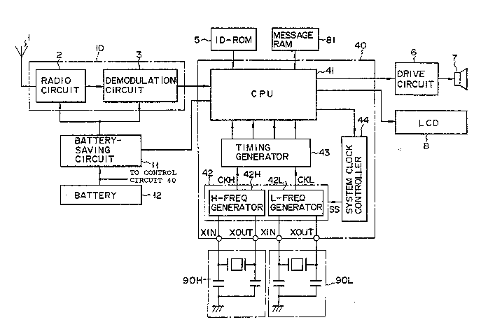
Fig. 1 schematically illustrates a pager receiver
according ts a first embodiment o~ the present
invention.
Referring to Fig. 1, an antenna 1 catches paging
signals which have been transmitted from a base station
tnot shown). The antenna 1 supplies the signals to a
receiver circuit 10 which comprises a radio circuit 2
and a demodulation circuit 3. The radio circuit 2
receives the paging signal and supplies it to the
demodulation circuik 3. The demodula-ti~n circuit 3
demodulates the paging signals and outputs the
83~7
demodulated signal to a control circuit 40. The control
circuit 40 collates the ID code contained in the paging
signals, with the ID aode assigned to the pager receiver and
stored in an ID ROM 5 connected to the control circuit 40.
If the ID codes are identical, the circuit 40 determines that
the pager has been paged, and generates an alarm signal to a
drive circuit 6. In response to the alarm signal, the
circuit 6 drives a loudspeaker 7. The loudspeaker 7
generates an alarm tone, in~orming a user o~ the pa~er
receiver that he is heing called. When the ID codes are
found to be identical, the control circuit 40 receives the
message code contained in the paging signal, corrects error
bits, if any, in the message code, and demodulates the
message code into message information. This information is
supplied from the control circuit 40 to an LCD (Liquid-
Crystal Display) 8. The message code is supplied from the
control circuit 40 to a message RAM 81 and stored therein.
The control circuit 40 is a single-chip IC comprising a
two-clock microcomputer (CPU) 41, a clock generator 42, a
timing generator 43, and a system-clock controller 44. The
CPU 41, which is the main component of the control circuit
40, has an arithmetic logic unit (ALU), an accumulator, an
instruction recorder, a program counter, various registers,
I/O ports, a program ROM, and a data RAM. The clock
- 12 -
high-frequency clock generator ~2H and a low~frequency clock
generator ~2L~ The high-frequency clock generator 42H is
connected by connecting terminals XIM and XOUT to a ceramic
oscillator 90H, whereas the low-frequency clock generator 42L
is connected by connecting terminals XIN and XOUT to a
ceramic oscillator 90L. These clock generators 42H and 42L
energize the ceramic oscillators 90H and 90L, respectively,
thereby generating a high-frequency (1.2MHz~ clock signal CKH
and a low-frequency (32KHz) clock signal CKL. The clock
generator 42 supplies these clock signals CKH and CKL to the
timing generator 43. The timing generator 43 frequency-
divides the high-frequency clock signal CKH and the low-
frequency clock signal CKL, thus generating system clock
signals which the CPU 41 requires. The CPU 41 supplies a
clock-setting co*n*unand to the system controll~r/ when
necessary~ In response to this command, the system-clock
controller 44 supplies a control signal S5 to the clock
generator 42. The high-frequency clock generator 42H and the
low-frequency clock generator 42L have an oscillation
start/stop control terminal each, and they are alternately
driven in accordance with the level of the control signal SS.
The pager receiver further comprises a battery-saving
circuit ~1. This circuit 11 operates as follows, in response
to the battery-saving control signal supplied from the
control circuit 40.
- 13 -
?~ 3 7
The circuit 11 supplies power from a battery 12 to the
receiver circuit 10 while the pager receiver is rec~iving
that group contained in the paging signal to which the pager
receiver belongs, thereby driving the recei.ver ~ircuit 10,
and supplies no power to the circuit 10 while the pager
receiver is receiving that any other group contained in the
paging signal, thus setting the circuit 10 in an inoperative
condition.
The operation of the pager receiver described above will
now be explained, with reference to the flow chart of Fig. 2
which explains operations of the CPU 41 in the control
circuit 40.
First, the user turns on the power switch (not shown) of
the pager receiver, whereby power is supplied from the power-
source unit (not shown, either) to the control circuit 40.
The CPU 41 of the circuit 40 initializes itself, and outputs
a low-frequency setting signal to the system-clock controller
44 in step 4a. In response to this signal, the system-clock
controller 44 supplies a control signal SS to the clock
generator 42, for driving the low-frequency clock generator
42L. As a result, the low-frequency clock generator 42L
starts outputting a low-frequency clock signal CKL, whereas
- 14 -
3 ~ ~
the high-freguency clock yenerator 42H remains in an
inoperative condition. The low-frequency c:Lock signal CRL is
supplied to the timing generator 43. The timing generator 43
generates a low-frequency system clock signal from the low
frequency clo~k ~ignal CKL, and supplies the system clock
signal to the CPU 41.
In step 4b, the CPU 41 outputs a battery-saving control
signal to the battery-saving circuit 11 so as to supply power
from the battery 12 to the receiver circuit 10. Upon a
receipt of the battery-saving control signal, the circuit 11
supplies power to the receiver circuit 10, whereby both the
radio circuit 2 and the demodulation circuit 3 go into
operation. Then, in step 4c, the CPU 41 determines whether
or not the pager receiver has detected a preamble word
consisting of a synchronization signal and a group
designation signal for identifying group signals to the
pager. If YES, the CPU 41 sets the timer (not shown~ in step
4d. More precisely, the timer is set when the synchroniza-
tion word in the paging signals for group 2 is received,assuming that the pager receiver belongs to group ~. The
timer will be automatically reset when the pager receiver
receives group 2 contained in the next frame of the paging
signal. In step 4e, the CPU 41 collates the ID code stored in
the ID-ROM 5 with the ID code contained in each calling word
for group 2.
- 15 -
~ 3 ~ rj ~
If the ID code stored in the ID-ROM 5 is identical with
the ID code contained in calling word 1, CPU 41 determines
that the pager receiver is being called. Then, the operation
goes to step 4j, in which the CPU 41 outputs a high-frequency
setting signal to the system-clock controller 44. In
response to this signal, the system~clock controller 44
supplie~ an oscillation start/stop control signal SS to the
clock generator 42, for driving the high-frequency clock
generator 42H. Thus, the clock generator 42H starts
outputting a high-fre~uency clock signal CKH, whereas the
low-frequency clock generator 42L is brought into an
inoperative condition, as is clearly shown in the timing
chart of Fig. 3. ~'he high-frequency clock signal CKH is
supplied to the timing generator 43. The timing generator 43
generates a high-frequency system clock signal from the high-
~requency clock signal CKH, and low-frequency clock generator
42L is supplies this system clock signal to the CPU 41.
Therefore, the CPU 41 is driven at a speed to correct error
bits, if any, in the message code which i5 contained in
calling word 1. In step 4k/ the receiver circuit 10 receives
the message code. In the next step, i.e., step 4*ir the CPU
41 corrects the message code.
Thereafter the operation goes to 5tep 4m, in which the
- 16 -
CPU 41 outputs a low-frequency setting signal to the system-
clock controller 44. In rasponse to this siynal the
controller 44 supplies an oscillation start/stop control
signal SS to the clock generator 42, for driving the low-
frequency clock yenerator 42L. As a result, the low-
frequency clock generator 42L starts outputting a low-
frequency clock signal CKL, whereas the high-frequency clock
generator 42H is set into an inoperative condition, as can be
seen in the timing chart of Fig. 3. The low frequency clock
signal CKL is supplied to the timing generator 43. The
timing yenerator 43 produces the low-frequency system clock
signal from the low-frequency clock signal CKL, and supplies
this system clock signal to the CPU 41. Therefore, the CPU
41 is then driven at a low speed.
In the next step, i.e. , step 4n, the CPU 41 outputs an
alarm signal to the drive circuit 6. In response to this
signal, the circuit 6 drives the loudspeaker 7. Thus, the
loudspeaker 7 generates a beep sound, informing the user of
the pager receiver that he or she is being called. At the
same time, the CPU 41 writes the message code into the
message RAM 81, and demodulates the message code into message
information and supplies this information to the LCD 8. The
LCD 8 displays the message information, whereby the user can
read the message sent from the caller.
- 17 -
~ 3~ ~ .3 ~
Thereafter, the operation goes to step 4f. In this step, the
CPU 41 determines whether or not the ID code stored in the
ID-ROM 5 has been collated with the ID codes contained in all
calling words of group 2 to which the pager receiver belongs.
5 If NO, the operation returns to step 4e, in which the ID code
in the ID-ROM 5 is collated with the ID code contained in the
next calling word. If YES in step 4f, that is, if the CPU 41
determines that all the ID codes included in group si~nals
consisting of calling words for group 2 have been checked,
the operation proceeds to step 4h. In step 4h, the CPU 41
outputs a battery-saving control signal to the battery saving
circuit 11 in order not to supply power to the receiver
circuit 10. Upon a receipt of this control signal, the
circuit 11 stops supplying power from the battery 12 to the
circuit 10. As a result, both the radio circuit 2 and the
demodulation circuit 3 are rendered inoperative, as can be
understood from Fig. 3. In other words, the pager receiver is
brought into a battery-saving condition, in which only the
CPU ~1 performs its function. In step 4i, the CPU 41
determines whether or not the time set by the timer (not
shown) has elapsed. If YES, the CPU 41 detects that the pager
receiver has just started rec*eiving the next frame. In this
case, the operation returns to step 4b. Steps 4b to 4n are
then executed, as has been explained,at this time for the
next frame.
- 18 -
~ 3 ~ 8 3 ~ 7
As has been described, it is the high-frequency clock
gene~ator 42H that operates while the pager recei~er is
receiving the message code contained in the calling word for
group 2 to which the pager receiver belongs, and it is the
low-frequency clock generator 42L that operate~ at all other
times.
If YE5 in step 4f, that is, if all the ID codes included
in a group signal consisting of calling words for groups 2
have been checked, the operation goes to step 4h. In step
4h, the CPU 41 causes the batterysaving circuit 11 to stop
supplying power to the receiver circuit 10. As a result, the
pager receiver is set into the battery-saving condition. In
other words, the low-frequency clock generator 42L continues
to operate as long as the pager receiver remains not called.
Since the high-frequency clock generator 42H operates
only while the pager receiver is receiving the message code
contained in calling word 1 of group2, and the low-frequency
clock generator 42L operates at all other times, the control
circuit 40 consumes less power than its counterpart of thP
prior-art pager receiver in which the high-frequency clock
generator operates all the time the whole frame of the paging
signal is rec*eived. Hence, the power consumption of the
-- 19 --
3 ~ ~
pager receiver is conserved and the battery can last lonyer.
Therefore, the running cost of the pager receiver may be
saved.
The first embodiment of the invention, which has been
described, can be modified in some ways. For example, as is
shown in Fig. 4, the high-frequency clock generator 42H can
be operated continuously while the pager receiver is
receiving the group 2 of the paging signal, and the low-
frequency clock generator 42L is operated while the pager
receiver is receiving any other group. In this case, too,
the pager receiver consumes less power than the conventional
one wherein the high-frequency clock generator continues to
operate all the time the entire frame of a paging signal is
received, and the battery lasts longer than in the
conventional pager receiver. Further, in this case, even if
the paging signal has been transmitted at a high speed, the
synchronization words contained in group 2 can be detected,
and the ID codes contained in the calling words in group 2
can be collated with the ID code stored in the ID-ROM 5.
Moreover, as is shown in Fig. 5, a clock generator 45H
can be coupled to the connecting terminal XIN of the high-
frequency clock generator 42H, and a clock generator 45L can
- 20 -
11 3~3~7
be coupled to the connecting terminal XIN o1E the low-
frequency clock generator 42L/ and the connecting terminals
XOUTs of the clock generators 42H and 42L can be made open.
In this instance, since tha terminals XOUTs are open, both
clock generators 42H and 42L are rendered inoperative, and
the clock signals output by the generators 45H and 45~ each
are supplied to the timing generator 43. The ¢lock
generators 45~ and ~5L have a terminal for receiving the
generation start/stop control signal SSO olltput from the
control circuit 40. Thus, the clock generators 45H and 45L
can be alternately operated in accordance with the level of
this control signal SSO~ Hence/ the control circuit 40 can
be driven by a high-frequency clock signal and a low-
fre~uency clock signal, provided that the circuit 40 supplies
the control signal SSO to the clock generators 45H and 45L in
steps 4b, 4j, and ~m of the ~low chart shown in Fig. 2. This
modified pager receiver also consumes less power than the
conventional one, thus lengthening the life~time of the
battery provided in it.
Second Embodiment
Fig. 6 schematically shows a pager receiver according to
a second embodiment of the present invention. ~he same
components as those shown in Fig. l are designated by the
same numerals.
- 21 -
The control circuit 400 of the pager rec~iver comprises
a CPU 410, a clock generator 420, a timing generator 430, and
a system clock controller ~40. The clock generator 420 has a
high-frequency clock generator 42H for generating a high-
frequency (1.2 ~Hz) clock signal C~I, a low-frequency clock
generator 42L for generating a low-fequency (32 KHz) clock
signal CKL, and an intermediate-frequency clock generator
4~M. The intermediate-frequency clock gen0rator 42M is
connected by connecting terminals XIN and XOUT to a ceramic
oscillator 90M. When driven, the clock generator 42M
energizes the ceramic oscillator 90M, thereby to generate an
intermediate-frequency clock signal CKM having a fre~uency
of, for example, 480 KHz. The timing generator 430 divides
the frequencies of the clock signals CKH, CKM, and CXL
generated by clock generators 42H, 42M, and 42L, forming
system clock signals which the CPU 410 requires. The system
clock controller 440 generates an oscillation control signal
SSP for selecting and driving one of thP clock generators
42H, 42M, and 42L, in accordance with a frequency-setting
signal output from the CPU 4100
The operation of the pager receiver, described above,
will now be explained with reference to the flow chart of
Fig. 7 which illustrates the operations of the CPU 410 in the
control circuit 400.
- 22 -
~83 ~
First, the user turns on the power switch (not shown) o~
the pager receiver, whereby power is supplied from the
battery 12 to the control circuit 400. The CPU 410 in the
circuit 400 initializes itself, and outputs a low-frequency
setting signal to the system-clock controller 440 in step 9a.
In response to this signal, the system-clock controller 440
supplies a control signal SSP to the clock generator 420, for
driving the low-frequency clock generator 42I,. As a result~
the low-frequency clock generator ~2L starts outputting a
low-frequency clock signal CKL, whereas the intermediate--
frequency clock generator 42M and the high-frequency clock
generator 42H remain in inoperative conditions. The low-
frequency clock signal CK~ is supplied to the timing
generator 430. The timing generator 430 generates a low-
frequency system clock signal from the low-frequency clock
signal CKL, and supplies the system clock signal to the CPU
410.
In step 9b, the CPU 410 outputs a battery-saving control
signal to a battery-saving circuit 11 so as to supply power
from the battery 12 to a receiver circuit 10. Upon receipt
of the battery-saving control signal, the battery-saving
circuit 11 supplies power to the receiver circuit 10, whereby
both the radio circuit 2 and demodulation circuit 3 in the
circuit 10 go into operation. Then, in step 9c, the CPU 410
- 23 -
~3~3~
outputs an intermediate-~requency setting signal to the
system-clock controller 440. In response to this signal, the
system-clock controller 4~0 supplies a control signal 5SP to
the clock generator 420, for driving the intermediat~-
frequency clock generator ~2~. Hence, only the intermediate-
frequency clock generator 42M is driven and starts outputting
an intermediatefrequency clock signal CICM, as is illustrated
in Fig. 8. This clock signal CKM is supplied to the timing
generator 430. The timing generator 430 generates an
intermediate-frequency system clock signal of the clock
signal CKM, and supplies this system clock signal to the CPU
410. As a result, the CPU 410 can operate at a higher speed
than when driven by the system clock signal produced from the
low-frequency clock signal CKL.
In step 9d, the CPU 410 determines whether or not the
pager receiver has detected the preamble word including a
synchronization word and the group designation signal within
a group signal. If YES, the CPU 410 sets the timer ~not
shown) in step 9e. More precisely, the timer is set when the
preamble word for group 2 is received, assuming that the
pager receiver belongs to group 2. The timer will be
automatically reset when the pager receiver receives group 2
contained in the next frame of the paging signal. In step
9f, the CPU 410 collates the ID code stored in an ID-ROM 5
with the ID code contained in each calling word for group 2.
- 24 -
If the ID code stored in the ID-ROM 5 is identical with
the ID code contained in calliny word 1, CPU 410 determines
that the pager receiver is being called. Then, the operation
goes to step 9k, in which the CPU 410 outpu1:s a high-
frequency setting signal to the system-cloclc controller 440.
In response to this signal, the system-clock controller 440
supplies an oscillation start/stop control signal SSP to the
clock generator 420, for driving the high-frequency clock
generator 42H. Thus, the clock generator 42H starts
outputting a high-frequency clock signal CKH. Hence, the
clock signal is switched from the intermediatefrequency clock
signal CKM to the high-frequency clock signal CXH, as is
shown in Fig. 8. The high-frequency clock signal CKH is
supplied to the timing generator 430. The timing generator
430 generates a highfrequency system clock signal from the
high~frequency clock signal CKH, and supplies this system
clock signal to the CPU 410. Therefore, the CPU 410 is
driven at a high speed to correct error bits, if any, in the
message code which is contained in calling word 1. In step 9
Q, the receiver circuit 10 receives the message code. In the
next step, i.e., step 9m, the CPU 410 corrects the message
code.
Theraafter, the operation goes to step 9n, in which the
CPU 410 outputs an intermediate-frequency setting signal to
- 25
~8~7
the system clock controller 440. In response to this signal,
the controller 440 supplies an oscillation start/stop control
signal SSP to the clock generator 420, for driving the
intermediate-frequency clock generator 42M. As a result, the
intermediatefrequency clock generator 42M sl:arts outputting
an intermediate-freguency clock signal CKM, as is understood
from Fig. 8. The clock ~ignal CKM i6 supplied to the timing
generator 430. The timing generator 430 produces an
intermediate-frequency system clock signal from the clock
signal CK*M, and supplies this system clock signal to the CPU
410. Therefore, the CPU 410 is driven at intermediate speed.
In the next step, i.e., 9o, the CPU 410 generates an
alarm signal to a drive circuit 6. In response to the alarm
signal, the circuit 6 drives the loudspeaker 7. Thus, the
loudspeaker 7 generates a beep sound, informing the user of
the pager receiver that he or she is being called. At the
same time, the CP~ 410 writes the message code into a message
RAM 81, and demodulates the message code into message
information and supplies this information to the LCD 8. The
LCD 8 displays the message information, whereby the user can
read the message sent from the caller.
Thereafter, the operation goes to step 9g. In this
- 26 -
3 ~ 7
step, the CPU 410 determines whether or not all the ID code
included in the group signal have been checked against the
stored ID codes. If NO, the op ration returns to step 9f, in
which the ID code in the ID-ROM 5 is collated with the ID
code contained in the next calling word. If YES in step ~g,
that is, if the CPU 410 determines that all the ID codes
included in the group signal have been checked against the
stored ID code, the operation proceeds to step 9h. In step
9h, the CPU 410 supplies a low-frequency setting signal to
~0 the system clock controller 440. In response to this signal,
the controller 440 outputs an oscillation start/stop signal
SSP to the clock generator 420. Hence, only the low-
frequency clock generator 42L operates, outputting a low-
frequency clock signal CKL to the timing generator 430. The
timing generator 430 generates a low-frequency system clock
signal from the clock signal CKL, and supplies the system
clock signal to the CPU 410 then. Therefore, the CPU 410
operates at a low speed.
In step 9i, the CPU 410 outputs a battery-saving control
signal to the battery-saving circuit 11 in order not to
supply power to the receiver circuit 10. Upon receipt of
this control signal, the circuit 11 stops supplying power
from the battery 12 to the circuit 10. As a result, both the
- 27 -
3 ~ ~
radio circuit 2 and the demodulation circuit 3 are rendered
inoperative, as can be understood from Fig~ 8. That is, the
pager receiver is brought into a battery-saving condition, in
which only the CPU 410 performs its function. In ~tep 9j,
the CPU 410 determines whether or not the time set to the
timer (not shown) has elapsed. If YES, the CPU 410 detects
that the pager receiver has just started receiving the next
frame. In this case, the operation returns to step 9b. Steps
9b to ~o are then executed, as has been explained, this time
for the next frame.
As has been described, it is the high-frequency clock
generator 42H that operates while the pager receiver is
receiving the message code contained in the calling word for
group 2 to which ~he pager receiver belongs, it i5 the
intermediate-frequency clock generator 42M that operates
while the pager receiver is receiving all other codes
contained in group 2, and it is the low-frequency clock
generator 42L that operatas while the pager receiver is
receiving any group other than group 2.
If YES in step 9f, that is, if all the ID codes included
in the group signal have been checked against the stored ID
code, the operation goes to step 9h. In step 9i, the CPU 410
causes the battery-saving circuit 11 to stop supplying power
- 28 -
~3~1 8.~7
to the receiver ciruit 10. As a result, the pager receiver
i5 set into th~ battery-saving condition. :rn other words,
the low-frequency clock generator ~2L continues to operate as
long as the pager receiver remains not called.
Since the high-fre~uency clock generator 42H operates
only while the pager receiver is receiving the message code
contained in calling word 1 of group2, and the intermediate-
frequency clock generator 42M or the low-frequency clock
generator 42L operates at all other times, the control
circuit 400 consumes less power than its counterpart of the
prior-art pager receiver in which the high-frequency clock
generator operates all the time the whole frame of the paging
signal is received. Hence, the power consumption of the
pager receiver is small, and the battery can last long~r.
Therefore, the running cost of the pager receiver is low.
Moreover, since the intermediate-frequency clock
generator 42M operates while the pager receiver is receiving
any code contained in group 2, other than the message code,
the CPU 410 is driven by the system clock signal generated
from the intermediate-frequency clock signal CKM to detect
the synchronization word and collate the ID codes. Hence,
the synchroniz.ation word can be reliably detected, and the ID
codes can be correctly collated, even if the paging signal is
transmitted at so high a speed that the CPU 410 fails to
29 -
~3~83~7
detect the synchronization word or to collate the ID codesaccurately when driven by the low-frequency system clock
signal.
In the above described embodiments, although
arrangements of a pager and its operation are explained in
detail, it is apparent to those skilled in the ant to apply
the present invention to a cordless telephone or a mobile
telephone~ Still, the present invention may be applied to a
signal processing unit of any kind of electronic equipment.
The present invention is not limited to the embodiments
described above. For instance, the structure of the clock
generators, the number thereof, the structure of the system
clock controller, and the sequence of controlling the clock
generatoxs can be altered in various ways, without departing
from the scope of the present invention.
- 3 o -