Language selection

Search

Patent 1318367 Summary

Third-party information liability

Some of the information on this Web page has been provided by external sources. The Government of Canada is not responsible for the accuracy, reliability or currency of the information supplied by external sources. Users wishing to rely upon this information should consult directly with the source of the information. Content provided by external sources is not subject to official languages, privacy and accessibility requirements.

Claims and Abstract availability

Any discrepancies in the text and image of the Claims and Abstract are due to differing posting times. Text of the Claims and Abstract are posted:

  • At the time the application is open to public inspection;
  • At the time of issue of the patent (grant).
(12) Patent: (11) CA 1318367
(21) Application Number: 1318367
(54) English Title: HIGH SPEED ECL INPUT BUFFER FOR VERTICAL FUSE ARRAYS
(54) French Title: TAMPON D'ENTREE ECL RAPIDE POUR RESEAUX PROTEGES PAR DES FUSIBLES VERTICAUX
Status: Expired and beyond the Period of Reversal
Bibliographic Data
(51) International Patent Classification (IPC):
  • H03K 19/17792 (2020.01)
  • G11C 08/08 (2006.01)
  • G11C 17/16 (2006.01)
  • H03K 19/018 (2006.01)
(72) Inventors :
  • WALLER, WILLIAM K. (United States of America)
  • LUICH, THOMAS M. (United States of America)
(73) Owners :
  • NATIONAL SEMICONDUCTOR CORPORATION
(71) Applicants :
  • NATIONAL SEMICONDUCTOR CORPORATION (United States of America)
(74) Agent: SMART & BIGGAR LP
(74) Associate agent:
(45) Issued: 1993-05-25
(22) Filed Date: 1989-09-29
Availability of licence: N/A
Dedicated to the Public: N/A
(25) Language of filing: English

Patent Cooperation Treaty (PCT): No

(30) Application Priority Data:
Application No. Country/Territory Date
306,780 (United States of America) 1989-02-03

Abstracts

English Abstract


27008/NSCO-5
A HIGH SPEED ECL INPUT BUFFER FOR
VERTICAL, FUSE ARRAYS
ABSTRACT OF THE DISCLOSURE
An ECL input buffer is particularly well-
suited for use with logic arrays where a large amount
of current must be sunk by the row line, for example,
when vertical fuse devices are used in an AND
array. The input buffer provides means for pulling
down the row line such that the entire amount of
current sunk by the input buffer from the row line
need not pass through a current source, thereby
minimizing current consumption of the input buffer.
A pull down current source is used which causes a
pull down transistor to turn on, thereby pulling down
the row line while requiring only the base current of
the pull down transistor to be consumed by the
current source. A pull up device is utilized and
means are included for insuring that the pull up and
pull down devices are not both turned on simultane-
ously, thereby preventing a current spike through the
pull up and pull down means.
APP:27008


Claims

Note: Claims are shown in the official language in which they were submitted.


72094-79
THE EMBODIMENTS OF THE INVENTION IN WHICH AN EXCLUSIVE
PROPERTY OR PRIVILEGE IS CLAIMED ARE DEFINED AS FOLLOWS:
1. A circuit comprising:
an input terminal for receiving an input signal;
an output terminal for providing an output signal
as a function of said input signal;
pull up means coupled between a pull up supply and
said output terminal;
pull down means coupled between a pull down supply
and said output terminal; and
pull down control means comprising:
a first current source; and
switch means operative in response to said input
signal and having a first current handling terminal coupled to
said current source and a second current handling terminal for
providing a pull down control signal to said pull down means,
wherein said pull down means comprises a first
transistor having a first current handling lead coupled to said
output terminal, a second current handling lead coupled to said
pull down supply, and a control terminal for receiving said pull
down control signal,
wherein said switch means of said pull down control
means comprises:
a second transistor having a first current handling
lead coupled to said first current source, a second current handl-
ing lead coupled to said control terminal of said first transistor,
and a control terminal;
- 12 -

72094-79
bias means coupled to said control terminal of said
second transistor; and
means for coupling said input signal to said first
current handling lead of said second transistor, and
wherein said bias means comprises a second current
source and a third transistor having a first terminal coupled to
a supply voltage, a second terminal coupled to said second current
source and to said control terminal of said second transistor,
and a control terminal coupled to a bias voltage.
2. A circuit comprising:
an input terminal for receiving an input signal;
an output terminal for providing an output signal as
a function of said input signal;
pull up means coupled between a pull up supply and
said output terminal;
pull down means coupled between a pull down supply
and said output terminal; and
pull down control means comprising:
a first current source; and
switch means operative in response to said input
signal and having a first current handling terminal coupled to
said current source and a second current handling terminal for
providing a pull down control signal to said pull down means,
wherein said pull down means comprises a first
transistor having a first current handling lead coupled to said
output terminal, a second current handling lead coupled to said
- 13 -

72094-79
pull down supply, and a control terminal for receiving said pull
down control signal,
wherein said switch means of said pull down control
means comprises:
a second transistor having a first current handling
lead coupled to said first current source, a second current
handling lead coupled to said control terminal of said first
transistor, and a control terminal;
bias means coupled to said control terminal of said
second transistor; and
means for coupling said. input signal to said first
current handling lead of said second transistor,
wherein said pull down control means comprises a pair
of transistors, each having a first current handling terminal
coupled in a common to a current source, a first transistor of
said pair of transistors also having a control terminal coupled
to said input terminal, a second transistor of said pair of
transistors also having a second current handling terminal coupled
to said control terminal of said pull down means, and a control
terminal connected to a bias potential.
3. A circuit comprising:
an input terminal for receiving an input signal;
an output terminal for providing an output signal
as a function of said input signal;
pull up means coupled between a pull up supply and
said output terminal;
- 14 -

72094-79
pull down means coupled between a pull down supply
and said output terminal; and
pull down control means comprising:
a first current source; and
switch means operative in response to said input
signal and having a first current handling terminal coupled to
said current source and a second current handling terminal for
providing a pull down control signal to said pull down means;
wherein said pull down means comprises a first
transistor having a first current handling lead coupled to said
output terminal, a second current handling lead coupled to said
pull down supply, and a control terminal for receiving said pull
down control signal,
wherein said switch means of said pull down control
means comprises:
a second transistor having a first current handling
lead coupled to said first current source, a second current
handling lead coupled to said control terminal of said first
transistor, and a control terminal;
bias means coupled to said control terminal of said
second transistor; and
means for coupling said input signal to said first
current handling lead of said second transistor,
which circuit further comprises additional means
coupled to said control terminal of said pull down means, said
additional means serving to pull up said control terminal of
said pull down means when said pull down control means is not
- 15 -

72094-79
pulling down said control terminal of said second transistor.
4. A circuit as in claim 3 wherein said additional means
comprises a pull up transistor having a first current handling
terminal coupled to a supply voltage, a second current handling
terminal coupled to said control terminal of said first transistor,
and a control terminal coupled to receive a control signal which
is a function of said input signal.
5. A circuit as in claim 4 wherein said additional means
further comprises a pair of transistors, each having a first
current handling terminal coupled in common to a third current
source, a first transistor of said pair of transistors also having
a control terminal coupled to said input terminal, a second
transistor of said pair of transistors also having a second current
handling terminal coupled to said control terminal of said
additional means, and a control terminal coupled to a bias
potential.
6. A circuit comprising:
an input terminal for receiving an input signal;
an output terminal for providing an output signal
as a function of said input signal;
pull up means coupled between a pull up supply and
said output terminal;
pull down means coupled between a pull down supply
and said output terminal; and
pull down control means comprising:
- 16 -

72094-79
a first current source; and
switch means operative in response to said input
signal and having a first current handling terminal coupled to
said current source and a second current handling terminal for
providing a pull down control signal to said pull down means,
wherein said pull down means comprises a first
transistor having a first current handling lead coupled to said
output terminal, a second current handling lead coupled to said
pull down supply, and a control terminal for receiving said pull
down control signal,
wherein said switch means of said pull down control
means comprises:
a second transistor having a first current handling
lead coupled to said first current source, a second current
handling lead coupled to said control terminal of said first
transistor, and a control terminal;
bias means coupled to said control terminal of said
second transistor; and
means for coupling said input signal to said first
current handling lead of said second transistor,
wherein said pull down control means comprises a
first pair of transistors, each having a first current handling
terminal coupled in a common to a current source, a first tran-
sistor of said first pair of transistors also having a control
terminal coupled to said input terminal, a second transistor of
said first pair of transistors also having a second current
- 17 -

72094-79
handling terminal coupled to said control terminal of said pull
down means, and a control terminal connected to a bias potential;
and
which further comprises additional means coupled to
said control terminal of said pull down means, said additional
means serving to pull up said control terminal of said pull down
means when said pull down control means is not pulling down said
control terminal of said second transistor, said additional means
comprising:
a pull up transistor having a first current handling
terminal coupled to a supply voltage, a second current handling
terminal coupled to said control terminal of said first transis-
tor, and a control terminal coupled to receive a control signal
which is a function of said input signal; and
a second pair of transistors, each having a first
current handling terminal coupled in common to a third current
source, a first transistor of said second pair of transistors also
having a control terminal coupled to said input terminal, a
second transistor of said second pair of transistors also having
a second current handling terminal coupled to said control terminal
of said additional means, and a control terminal coupled to a
bias potential.
7. A circuit as in claim 6 wherein said control
terminals of said second transistors of said first and second pair
of transistors are coupled to the same bias potential.
8. A circuit as in claim 7 wherein said pull up means
- 18 -

72094-79
comprises a transistor having a first current handling lead
connected to said pull up supply, a second current handling lead
connected to said output terminal, and a control terminal.
9. A circuit as in claim 8 which further comprises pull
up control means responsive to said input signal and having an
output lead connected to said control terminal of said transistor
of said pull up means.
10. A circuit as in claim 9 wherein said pull up control
means comprises a pair of transistors, each having a first
current handling terminal coupled in common to a current source,
a first transistor of said pair of transistors also having a
control terminal coupled to said input terminal, a second transis-
tor of said pair of transistors also having a second current
handling terminal coupled to said control terminal of said
transistor of said pull up means, and a control terminal coupled
to a bias potential.
11. A circuit comprising:
an input terminal for receiving an input signal;
a pair of complementary output terminals for
providing a complementary output signal as a function of said
input signal;
a pair of pull up means, each coupled between a pull
up supply and a respective one of said output terminals;
a pair of pull down means, each coupled between a
pull down supply and a respective one of said output terminals;
and
- 19 -

72094-79
a pair of pull down control means, operating out
of phase and each comprising:
a first current source; and
switch means operative in response to said input
signal and having a first current handling terminal coupled to
said current source and a second current handling terminal for
providing a pull down control signal to an associated one of said
pull down means.
12. A circuit as in claim 11 wherein each of said pull
down means comprises a first transistor having a first current
handling lead coupled to a respective one of said output terminals,
a second current handling lead coupled to said pull down supply,
and a control terminal for receiving a respective one of said pull
down control signals.
13. A circuit as in claim 12 wherein said switch means
of each of said pull down control means comprises:
a second transistor having a first current handling
lead coupled to said first current source, a second current
handling lead coupled to said control terminal of said first
transistor, and a control terminal;
bias means coupled to said control terminal of said
second transistor; and
means for coupling said input signal to said first
current handling lead of said second transistor.
14. A circuit as in claim 13 wherein said bias means
- 20 -

72094-79
comprises a second current source and a third transistor having
a first terminal coupled to a supply voltage, a second terminal
coupled to said second current source and to said control
terminal of said second transistor, and a control terminal
coupled to a bias voltage.
15. A circuit as in claim 13 wherein each of said pull
down control means comprises a pair of transistors, each having a
first current handling terminal coupled in a common to a current
source, a first transistor of said pair of transistors also
having a control terminal coupled to said input terminal, a
second transistor of said pair of transistors also having a second
current handling terminal coupled to said control terminal of
said pull down means, and a control terminal connected to a bias
potential.
16. A circuit as in claim 13 which further comprises a
set of additional means, each coupled to said control terminals
of a respective one of said pull down means, said additional means
serving to pull up said control terminal of said pull down means
when said pull down control means is not pulling down said con-
trol terminal of said second transistor.
17. A circuit as in claim 16 wherein each said additional
means comprises a pull up transistor having a first current
handling terminal coupled to a supply voltage, a second current
handling terminal coupled to said control terminal of said first
transistor, and a control terminal coupled to receive a control
- 21 -

72094-79
signal which is a function of said input signal.
18. A circuit as in claim 17 wherein each said additional
means further comprises a pair of transistors, each having a
first current handling terminal coupled in common to a third
current source, a first transistor of said pair of transistors
also having a control terminal coupled to said input terminal, a
second transistor of said pair of transistors also having a
second current handling terminal coupled to said control terminal
of said additional means, and a control terminal coupled to a
bias potential.
19. A circuit as in claim 13 wherein:
each pull down control means comprises a first pair
of transistors, each having a first current handling terminal
coupled in a common to a current source t a first transistor of
said first pair of transistors also having a control terminal
coupled to said input terminal, a second transistor of said first
pair of transistors also having a second current handling ter-
minal coupled to said control terminal of an associated use of
said pull down means, and a control terminal connected to a bias
potential; and
which further comprises a pair of additional means,
each coupled to said control terminal of an associated one of said
pull down means, said additional means serving to pull up said
control terminal of said pull down means when said pull down
control means is not pulling down said control terminal of said
second transistor, each said additional means comprising:
- 22 -

72094-79
a pull up transistor having a first current handling
terminal coupled to a supply voltage r a second current handling
terminal coupled to said control terminal of said first transistor,
and a control terminal coupled to receive a control signal which
is a function of said input signal; and
a second pair of transistors, each having a first
current handling terminal coupled in common to a third current
source, a first transistor of said second pair of transistors also
having a control terminal coupled to said input terminal, a
second transistor of said second pair of transistors also having
a second current handling terminal coupled to said control terminal
of said additional means, and a control terminal coupled to a
bias potential.
20. A circuit as in claim 19 wherein said control ter-
minals of said second transistors of said first and second pair
of transistors are coupled to the same bias potential.
21. A circuit as in claim 20 wherein said pull up means
comprises a transistor having a first current handling lead
connected to said pull up supply, a second current handling lead
connected to an associated one of said output terminals, and a
control terminal.
22. A circuit as in claim 21 which further comprises a
pair of pull up control means, each responsive to said input
signal and having an output lead connected to said control
terminal of said transistor of an associated one of said pull up
means.
- 23 -

24 72094-79
23. A circuit as in claim 22 wherein each of said pull up
control means comprises a pair of transistors, each having a first
current handling terminal coupled in common to a current source, a
first transistor of said pair of transistors also having a control
terminal coupled to said input terminal, a second transistor of
said pair of transistors also having a second current handling
terminal coupled to said control terminal of said transistor of
said pull up means, and a control terminal coupled to a bias
potential.
24. A circuit as in claim 12 wherein each of said pull down
control means comprises a pair of transistors, each having a first
current handling terminal coupled in a common to a current source,
a first transistor of said pair of transistors also having a
control terminal coupled to said input terminal, a second
transistor of said pair of transistors also having a second
current handling terminal coupled to said control terminal of said
first transistor of an associated one of said pull down means, and
a control terminal connected to a bias potential.
25. A circuit as in claim 12 wherein said pull down control
means comprises:
a second pair of transistors each having a first current
handling lead coupled to said first current source, a second
current handling lead coupled to said control terminal of said
first transistor of an associated one of said pull down means, and
a control terminal;

72094-79
bias means coupled to said control terminal of a first one of
said second pair of transistors; and
means for coupling said input signal to said control terminal
of a second one of said second pair of transistors.
26. A circuit as in claim 25 wherein said bias means
comprises a second current source and a third transistor having a
first terminal coupled to a supply voltage, a second terminal
coupled to said second current source and to said control terminal
of said first one of said second pair of transistors, and a
control terminal coupled to a bias voltage.
27. A circuit as in claim 25 which further comprises a set
of additional means, each coupled to said control terminal of a
first transistor of an associated one of said pull down means,
said additional means serving to pull up said control terminal of
a first transistor of an associated one of said pull down means
when said pull down control means is not pulling down said control
terminal of said first transistor.
28. A circuit as in claim 27 wherein each said additional
means comprises a pull up transistor having a first current
handling terminal coupled to a supply voltage, a second current
handling terminal coupled to said control terminal of a first
transistor of an associated one of said pull down means, and a

26 72094-79
control terminal coupled to receive a control signal which is a
function of said input signal.
29. A circuit as in claim 28 wherein each said additional
means further comprises a pair of transistors, each having a first
current handling terminal coupled in a common to a third current
source, a first transistor of said pair of transistors also having
a control terminal coupled to said input terminal, a second
transistor of said pair of transistors also having a second
current handling terminal coupled to said control terminal of said
pull up transistor and said second transistor having a control
terminal coupled to a bias potential.
30. A circuit as in claim 12 wherein
said pair of pull down control means comprises
a second transistor having a first current handling terminal
coupled to said control terminal of a first transistor of an
associated one of said pull down means, a second current handling
terminal coupled to said first current source, and a control
terminal coupled to said input terminal;
a third transistor having a first current handling terminal
coupled to said control terminal of a second transistor of an
associated one of said pull down means, a second currant handling
terminal coupled to said first current source, and a control
terminal coupled to a bias potential;
which further comprises:

27 72094-79
a first pull up transistor having a first current handling
terminal coupled to a supply voltage, a second current handling
terminal coupled to said control terminal of said first transistor
of an associated one of said pull down means, and a control
terminal coupled to receive a control signal which is a function
of said input signal;
a second pull up transistor having a first current handling
terminal coupled to a supply voltage, a second current handling
terminal coupled to said control terminal of said second
transistor of an associated one of said pull down means, and a
control terminal coupled to receive a control signal which is a
function of said input signal;
a fourth transistor having a first current handling terminal
coupled to a second current source a second current handling
terminal coupled to said control terminal of said first pull up
transistor and a control terminal coupled to said input terminal;
and
a fifth transistor having a first current handling terminal
coupled to said second current source, a second current handling
terminal coupled to said control terminal of said second pull up
transistor, and a control terminal coupled to a bias potential.
31. A circuit as in claim 30 wherein said control terminals
of said third and fifth transistors are coupled to the same bias
potential.

28 72094-79
32. A circuit as in claim 31 wherein each of said pull up
means comprises a transistor having a first current handling lead
connected to said pull up supply, a second current handling lead
connected to an associated one of said output terminals, and a
control terminal for receiving a control signal as a function of
said input signal.

Description

Note: Descriptions are shown in the official language in which they were submitted.


3 ~ r~
1 7~094-79
A HIGH SP~D ECL INPUT BU~FER FOR VLRTICAL FUSE ARRAYS
FIELD OF THE INV NTIO~
This invention pertains to clrcuitry for driving fuse
programmable arrays, and which is particularly well su.ited for
driving fuse arrays utilizing vertical fuses.
BRTEF DESCR~IPTIO~ OF THE: DRhWINGS
Figure 1 is a diagram depicting a typical prior art
lateral fusei
Figure 2 is a schematic diagram depicting a typical
prior art OR array utilizing lateral fuses;
Figure 3 is a schematic diagram of a prior art input
buffer suitable for use in driving the row line of the array of
Figure 2;
Figure 4a is a cross sectional view of a floating base
bipolar transistor used as a vertical fuse device of the prior
art;
Figure 4b is a schematic representation of the
unprogrammed and programmed states of the vertical fuse device of
Figure 4a;
Figure 5 is a schematic diagram of an "AND" array; and
Figure 6 is a schematic diagram of one embodiment of a
novel input buffer constructed in accordance with the teachings of
this lnvention.
ACKGROUND
Arrays of iuse devices, and more particularly, arrays
fabricated utilizing emitter coupled logic ~ECL) technology are
well known in the prior art. Such fuse arrays are suitable for

1 3~ ~3~
la 72094-79
orming program~able read only memories ~PROMs) and pro~rammable
logic arrays (PLAs). Emitter coupled logic technology is
particularly well sulted for extremely fast devices since opposing
transistors are forced to share a limited amoun~ of current made
available by a current source in such a manner that neither of the
two transistors ever saturate.
One fuse element suitable for use in such devices is the
so-called lateral fuse, such as the metal fuse depicted in Figure
1 which may be formed of any suitable metal or interconnect
material, typically titanium tungsten. When utilizing a lateral
fuse device with ECL circuitry, the most appropriate fuse array
configuration is the OR configuration, since the ECL input (which
has limited current sink capability) will only sink transient
(capacitive) current. Such an OR array is shown in ~he schematic
diagram of Figure 2. Figure 2 shows a plurality of N columns 204-
1 through 204-N each
,.. .
,~ . ,

~3~3~
containing a current source 206-1 through 206-N
tending to pull nodes 209~1 through 209-N low. Row
line 201 serves to receive an input signal which is
supplied to the base of transistors 202-1 through
202-N, having their collectors connected to VCC and
their emitters connected through fuses 203-1 through
203-N to node 209-1 through 209-N. Fuses 203-1
through 203-N are capable of being individually
programmed (i.e., altered from their initial state of
being short circuits to a programmed state of ~eing
an open circuit) in a well known manner, for example
by providing a high signal on row line 201 and
providing a programming voltage in excess of VCC and
typically 10 volts to the collectors of those of
transistors 202-1 through 202-N associated with those
of fuses 203-1 through 203-N which are desired to be
programmed.
A single current source circuit containin~
transistor load device 207 and resistor 203 serYes to
supply current from a positive supply voltage VCC
through diodes 205-1 to 205-N to nodes 209-1 through
209-N. Resistor 208 supplies current required by
current sources 206-1 through 206-N when such current
is not supplied by transistors 202-1 through 202-N.
This occurs when row line 201 goes low, or a fuse
203-1 through 203-N associated with a particular
current source 206-1 through 206-N is blown (open).
Transistor 207 serves to limit the voltage across
resistor 208 when more than one current source 206-1
through 206-N is drawing current from ~CC at the same
time.
One embodiment of a circuit suitable for
providing appropriate driving signals to row line 201
is shown in the schematic diagram of Fig. 3. Row
driver circuit 300 is an ECL circuit utiliziny a

first current source 310 to control pull up
transistors 306 and 314 which serve to supply pull up
current to ROW line 308 and ROW line 315,
respectively. Circuit 300 includes a second current
source 312 which serves to control pull down
transistors 304 and 313 which serve to sink current
from ROW line 308 and ROW line 305, respectively. An
illpUt signal defines whether it is desired to source
~urrent to row line 315 (i.e., apply a logical one
signal to row line 315) or sink curr nt from row line
315 (i.e., apply a logical zero signal to row line
315~, and simultaneously apply the inverse binary
signal to ROW line 308. Input lead 301 is connected
to the base of transistor 302, having its collector
connected to VCC. The emitter of transistor 302 is
connected to pull ~own current source 303 and to the
bases of transistors 304 and 305. In a similar
manner, a bias voltage VBB having a value
approximately between a logical zero and a logical
one voltage level of the input signal applied to
input lead 301, is applied to the base of transistor
316. The collector of transistor 316 is connected to
VCC, and its emitter is connected to pull down
current source 317 and to the bases of transistors
311 and 313. Thus, as is well known to those of
ordinary skill in the art of ECL circuit design, when
the input signal applied to input lead 301 is low
~i.e, less than VBB) transistors 304 and 305 are
turned off and transistors 311 and 313 are turned
on. With transistors 304 and 305 turned off, current
is supplied from VCC through resistor 307 to the base
of transistor 306, turning on transistor 306 and
applying current to ROW line 308, thus providing a
logical one signal to ROW line 308. Similarly, with
transistors 311 and 313 turned on, the voltage

4 ~ 3 ~
applied to the base of row line pull up transistor
314 is low, keeping row line pull up transistor 314
turned off. At the same time, transistor 313 is
turned on, thus pulling row line 315 low, to a
logical zero value.
Since ECL input buffer 30~ includes active
pull up transistors 306 and 314 having low output
impedance, and pulls down by way of current source
312 having medium to high output impedance, circuit
300 is very effective in driving the high input
impedance of row line 201 of the emitter follower
array of Fig. 2. Since no DC current is sourced by
row line 201 of Fig. 2, ECL buffer 300 of Fig. 3 need
only sink capacitive current frQm row line 201. This
is acceptable, since the medium to high input
impedance of circuit 300 is eapable of providing only
- small currents. Conversely, a small DC current is
sunk by row line 201, in the amount of the sum of the
current supplied current sources 206-1 through 206-N,
divided by the current gain or beta of transistors
~202-1 through Q202-N, respectively. This small
amount of DC current which is sunk by row line 201 is
easily provided by the low output impedance of
transistors 306 and 314 of the buffer of Fig. 3.
An alternative to the lateral fuse device of
Fig. 1 is the so-called vertical fuse, as depicted in
cross-sectional view in Fig. 4a. Vertical fuse 40 of
Fig. 4a is well known in the prior art and includes
buried collector 41, substrate 42, base region 43,
and emitter 44. Base region 43 is doped to an
opposite conductivity type as buried collector 41,
substrate 42, and emitter 44, thereby forming a
vertical bipolar transistor. When used as a fuse
device, emitter 44 and buried collector 41 serve as
the two leads of the fuse device and, in its

5 13~3~
unprogrammed state, remains an open circuit.
However, fuse device 40 is capable of being
programmed, for example by the application of a
sufficient amount of programming current applied at a
sufficiently high voltage to cause breakdown of the
PN junction formed between emitter 44 and base 43.
When this happens, emitter 44 and base 43 become
shorted, with the result that a PN diode, rather than
an open circuit, is rormed between the two terminals
of fuse device 40, i.e., emitter 44 and buried
collector 41. The use of a vertical fuse device
comprising a floating base bipolar transistor forming
an open circuit when unprogrammed and which models a
diode when programmed is depicted in Fig. 4b.
Vertical fuse arrays form a diode "AND"
configuration, as shown in Fig. S. Array S00
includes row line 501 and columns 503~1 through 503-
N. Connected between row line 501 and columns 503-1
through 503-~ are vertical fuse elements 502-1
through 502-N, respectively. Columns 503-1 through
503-~ are applied with current ~rom VCC terminal 504
through resistors 505-1 through 505-N,
respectively. Transistors 506-1 through 506-N have
their bases connected to columns 503-1 through 503-N,
their collectors connected to VCC, and their emitters
connected in common to the input lead of sense
amplifier 507. In this manner, sense amplifier 507
provides an output signal on output lead 510
indicating whether all of fuses 502-1 through 502-N
have been programmed (i.e., changed from an open
circuit to a diode providing a short circuit between
columns 503-1 through S03--N to row line 501). In
other words, when any one or more of fuses 502-1
through 502-N remain unprogrammed (open circuit), the
associated column is not pulled low, turning on the

6 ~ 3 ~
associated one of transistors 506-1 through 506-N,
and causing sense amplifier 507 to provide a logical
one output signal on output lead 510. Conversely,
when all of fuses 502-1 through 502-N are programmed
to provide a short circuit between columns 503-1
through 503-N to row line 501, columns 503~-1 through
503-N are all pulled low, thereby preventing any of
transistors 506-1 through 506-N from turning on,
causing sense amplifier 507 to provide a logical zero
output signal on output lead 510.
As is the case with OR array 200 of Fig. 2,
row line 501 must be driven by an input buffer
circuit. Row line 501 can be driven by input buffer
circuit 300 of Fis. 3, but only if pull down current
qource 312 is made sufficiently large. For example,
in the AND array of Fig. 5, the current flowing from
each column 503-1 through 503-N through a programmed
fuse 502-1 through 502-M to row line 501 is approxi-
mately 0.5 milliamps. For a typical PLA array havingapproximately 64 columns, each row line must sink
between 15 to 30 milliamps. However, typical PLA
devices include a plurality of row lines allowing for
greater sophistication of the PLA. For a typical PLA
having 16 row lines, the current drain for the 16
current sources alone is approximately 240 to 480
milliamps, a considerable amount of power. Accord-
ingly, there arises the need for minimizing the power
consumption of ECL PLAs utilizing an AND array of
fuse devices.
SUMMARY
In accordance with the teachings of this
invention, a novel ECL input buffer is provided which
is particularly well-suited for use with logic arrays
where a large amount of current must be sunk by the

1 3 iL ~ 3 ~eJ ~
7 720g~L-79
row line, for example, when vertical fuse devices are used in an
AND array. In accordance with the teachin-Js of this invention,
the input buffer provides means for pulling down ~he row line such
that the entire amount of current ~unk by the input buffer from
the row line need not pass through a current source, thereby
minimizing currant consumption of the input buffer. In one
embodiment of this invention, a pull down current source is used
which, in response to an appropriate level of an input signal
applied to the input buffer~ causes a pull down transistor to turn
on, thereby pulling down the row line while requirlng only the
base current of the pull down transistor to be consumed by the
curren~ source. In one embodiment of this invention, a pull up
device is utilized and means are included for insuring that the
pull up and pull down devices are not both turned on
simultaneously, thereby preventing a current spike through the
pull up and pull down devices.
According to a bxoad aspect of the invention there is
provided a circuit comprising:
; an input terminal for receiving an input signal;
an output terminal for providing an output signal as a
function of said input signal;
pull up means coup~ed hetween a pull up supply and said
output terminal;
pull down means coupled between a pull down supply and
said output terminal; and
pull down control means comprising:
a first current source; and
,,~

~l 3~$3~
8 72094-7g
swltch means operative in response to said input signal
and having a first current handling termina]. coupled to said
current source and a second current handling terminal for
providing a pull down con~rol signal to said pull down means,
wherein said pull down means comprises a flrst
transistor having a first current handl.ing ].ead coupled to said
output terminal, a second current handling lead coupled to said
pull down supply, and a control terminal for receiving said pull
down control signal,
wherein said switch means of said pull down control
means comprises:
a second transistor having a first current handling lead
coupled to said first current source, a second current handling
lead coupled to said control texminal of said first transistor,
and a control terminal;
bias means coupled to said control terminal of said second
tran~istor; and
means for coupling said input signal to said first current
handling lead of said second tran3istor, and
; 20 wherein said bias means comprises a second current source and
a third transistor having a first terminal coupled to a supply
voltage, a second terminal coupled to said second current source
and to said control terminal of said second transistor, and a
control terminal coupled to a bias vo].~age.
According to another broad aspect of the invention there
ls provided a circuit comprising,
an input terminal for receiving an input signal;

8a 72094-79
an output terminal for providing an output signal as a
function of said input signa].;
pull up means coupled hetween a pull up supply and said
output terminal;
pull down means coupled between a pull down supply and
said output terminal; and
pull down control means comprising:
a first current source; and
switch means operative in response to said input signal
and having a first current handling terminal coupled to said
current source and a second current handling terminal for
providing a pull down control signal to said pull down means,
wherein said pull down means comprises a fi:rst
transistor having a firs~ current handling lead coupled to said
output terminal, a second current handling lead coupled to said
pull down supply, and a control terminal for receiving said pull
down control signal,
wherein said switch means of said pull down control
means comprises:
a second transistor having a first current handling lead
coupled to said first current souxce, a second current handling
lead coupled to said control tPrminal of said first transistor
and a control terminal;
bias means coupled to said control terminal of sald second
transistor; and
means for coupling said input signal to said first current
handling lead of said second transistor,
"

13~
8b 7~09~-79
wherein said pull down control means comprises a pair of
transistoxs, each having a first current handling terminal coupled
in a common to a cu.rrent source, a first transistor of said pair
of trànsistors also having a control termlnal coupled to said
input terminal, a seconA transistor of said pair of transistors
also having a second current l-andling terminal coupled to said
control terminal of said pull down means, and a control terminal
connected ~o a bias poten~ial.
According to another broad aspect of the invention there
is provided a clrcuit comprising:
an input terminal for receiving an input signal;
an ou-tput terminal for providing an output siynal as a
function of saicl input signal;
pull up means coupled between a pull up supply and said
output terminal;
pull down means coupled between a pull down supply and
said output terminal; and
pull down control means comprising:
a first current source; and
20 switch means operative in response to said input signal
and having a first current handling terminal coupled to said
current source and a second current handling terminal for
providing a pull down control signal to said pull down means,
wherein said pull down means comprises a first
transistor having a first current handling lead coupled to said
output terminal, a second current handling lead coupled to said
pull down supply, and a control terminal for recelving said pull
, ~

~3~3~
8c
7209~-79
down control signal,
wherein said switch maans of said pull down control
means comprises:
a second transistor having a first current handling lead
coupled to said first current source~ a secolld current handliny
lead coupled to said control terminal of said first transistor,
and a control terminal;
bias means coupled to said control terminal of said second
transistor; and
means for coupling said input signal to said first current
handling lead of said second translstor,
which circuit further comprises additional means coupled to
said control terminal of said pull down means, said additional
means serving to pull up said control terminal of said pull down
means when said pull down control means is not pulling down said
control terminal of said second transistor.
According to another broad aspect of the invention there
is provided a circuit comprising5
an input terminal for receiving an input signal;
an output terminal for providiny an output signal as a
function of said inpuk signal;
pull up means coupled between a pull up supply and said
outpu~ terminal;
pull down means coupled between a pull down supply and
said output terminal; and
pull down control means comprisiny,
a first current source; and
,..~ I

~ 3 ~ P~
8d 72094-79
switch means operative in response to said input signal
and having a first current handling terminal coupled to said
cuxrent source and a second current handllng terminal for
providing a pull down control signal to said pull down means,
wherein said pull down means comprises a first
transistor having a first current handling :lead coupled to sald
output terminal, a second current handling :Lead coupled to said
pull down supply, and a control terminal for receiving said pull
down control slgnal,
wherein said switch means of said pull down control
means comprises:
a second transistor having a first current handling lead
coupled to said first current source, a second current handling
lead coupled to said control terminal of said first transistor,
and a control terminal;
bia3 means coupled to said control ter~inal of said second
transistor; and
means for coupling said input signal to said first current
handling lead of said second transistor,
w~erein said pull down control means comprlses a first pair
of transistors, each having a first current handling terminal
coupled in a common to a current source, a first transistor of
said first pair of transis~ors also having a con~rol ~erminal
coupled to said input terminal, a second transistor of said first
pair of transistors also having a second current handling terminal
coupled to said control terminal of said pull down means, and a
control terminal connected to a bias potential; and

~ 3 ~
8e 72094-79
~ hich further comprise~ additional means coupled to said
control terminal of said pull down means, said additional means
serving to pull up said control terminal of said pull do~n means
when said pull down control means is not pulllng down said control
terminal of said second transistor, said additional means
comprising:
: a pull up transistor having a first current handling
terminal coupled to a supply voltage, a second current hanclling
terminal coupled to said control terminal of said first
transistor, and a control terminal coupled to receive a control
signal which is a function of said input signal; and
a seconcl pair of transistors, each having a first
current handling terminal coupled in common to a third current
source, a first transistor of said second pair of transistors also
having a control terminal coupled to said input terminal, a second
transistor of said second pair of transistors also having a second
curren~ handling terminal coupled to said control terminal of said
additional means, and a control terminal coupled to a bias
potential.
According to another broad aspect of the invention there
is provided a circuit comprising:
an input terminal for receiving an input signal;
a pair of complementary output terminals for providing a
complementary output signal as a function of said input signal;
a pair of pull up means, each coupled between a pull up
supply and a respective one of said output terminals;

~ 3 1 ~
~f 72~94-79
a pair of pull down means, each coupled between a pull down
supply and a respective one of said output terminals; and
a pair of pull down control means, opera~ing out of phase and
each comprising,
a first current source; and
switch means operakive in response to said input signal
and having a first current handling termina:L coupled to said
current source and a second current handling terminal for
providing a pull down control signal to an associated one of said
pull down means.
According to another broad aspect of the invention there
is provided a circuit comprising 5
an input terminal for receiving an input signal;
a pair of complementary output terminals for providing a
complementary output signal as a function of said inpu~ signal;
a pair of pull up means, each coupled batween a pull up
supply and a respective one of said output terminals;
a pair of pull down means, each coupled between a pull down
supply and a respective one of said output terminals; and
a pair of pull down control means, operating out of phase and
each comprising,
a ~irst current source and
switch means operative in response to said input signal
and havlng a first current handling terminal coupled to said
current source and a second current handllng terminal for
provlding a pull down control signal ko an associated one of said
pull down me~ns.
~s~

~ 3 ~ s~ ~
8g 72094-79
DETAIL~D D~SCRfPTION
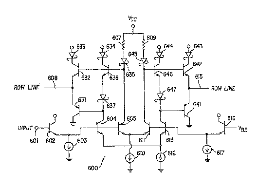
Referring -to Figure 6, an .input siynal ls appliecl to
input lead G01, and a bias voltage VB~ iY applied to the base of
transistor 616, with the bias voltage having a voltage level
between the vol~age leval of a logical zero and logical one input
signal applied to lnput lead 601. Current source 610 i~ used to
control the pull up devices and current source 612 is used to
control the pull down devices. ECL transistor pairs 605, 611; and
604, 613 are used to steer current from current sources 610 and
612, respectively, in response to the input signal. With a
logical one input signal applied to input lead 601, transistor 602
turns on, and current from current sources 612 and 610 are steered
through transistor 604 and 605 7 respectively. With no current
passing through translstor 611, the base o~ pull up transistor 642
is pulled high through the path from VCC through resistor 609 and
Schottky dioda 645. This causes transis~or 642 to turn on,
applying current from VCC through Schottky diode 643, through
transistQr 642, to ROW line 615, there~y pulling up ROW line 615.
At the same time, ROW line 608 is pulled low in a manner which
will be readily understood wi~h reference to the operatiGn of the
circuit to pull down ROW line 615.
Conversely, with a logical zero input signal applied to
input terminal 601, transistor 602 turns off, and current is
steered from current sources 612

9 :~ 3 ~
and 610 through transistor 613, and 611~
respectivelyO With current being pulled through
transistor 611, the base of transistor 642 is pulled
low, thereby turning off transistor 642 and current
is no longer supplied to pull up row line 615. With
current flowing through transistor 613, the base of
transistor 641 is pulled lower, thereby turning on
PNP transistor 641 and in turn sinking current from
row line 615, thus pulling down row line 615. Of
importance~ pull down current source 612 need only
sink a relatively small amount of current, i.e., the
base current of pull down transistor 641. For a
typical PNP transistor 641 having a beta of 1~, only
1.5 milliamps of base current is needed to cause a 15
milliamp pull down current from row line 615. Thus,
the magnitude of current which must be sunk by
current source 612 is significantly less than the
desired amount of pull down current ~rom the row
line.
In one embodiment of this invention, the
base of pull down transistor 641 is connected to the
emitter of transistor 646 with a direct connection
(not shown~. In the embodiment shown in Fig. 6, the
base of transistor 641 is connected to the emitter of
transistor 646 via Schottky diode 647, thereby
reducing the change in voltage applied to the base of
transistor 646 required to cause transistors 641 and
642 to switch, thereby increasing switching speed.
Thus, with a high input signal applied to input lead
601 transistors 611 and 613 are off, the bases of
transistors 646 and 642 are high, transistor 641 has
no base current and thus is off, as is transistor 646
since it has no emitter current. At this time,
transistor 642 is turned on, pulling up row line 615.
Conversely, with a low input signal applied

10 ~L3~
to input lead 601, transistors 611 and 613 are on,
the bases of transistors 646 and 6~2 are low,
transistor 642 is off, and row line 615 is pulled
down through conducting transistor 641. At this
time, the voltage applied to row line 1il5 is equal to
VB(642) - V~E(646) - V~(647) ~ VBE(641) =
VB(642) - Vf, wh~x~
VB(642) is the base voltage of transistor
642;
VBE(646) is the base-emitter voltage of
transistor 646;
VBE(641) is ~he base-emitter voltage of
transistor 641 which is equal to VBE(646); and
Vf(647) is the forward voltage drop across
Schottky transistor 647.
In one embodiment of this invention, as
depicted in Fig. 6, Schottky diodes 633, 634~ 643 and
644 are connected between VCC and the colleotors of
transistors 632, 636, 642, and 646, respectively, in
order to prevent breakdown during programming.
During programming, any deselected row may be pulled
much higher than VCC (typically to about 10 volts).
Schottky diodes 633, 634, 643 and 644 block any
breakdown path to VCC which might otherwise occur due
to the reverse breakdown voltage between the emitter
and collector (B~ECR) of transistors 646 and 642, or
the emitter base breakdown voltage (BVEBO~ through
- resistor 609 to VCC.
Although the foregoing invention has been
described in some detail by way of illustration and
example for purposes of clarity of understanding, it
will be readily apparent to those of ordinary skill
in the art in light of the teachings of this
application that certain changes and modifications
may be practiced within the scope of the appended

11 1 31~367
cla im .

Representative Drawing
A single figure which represents the drawing illustrating the invention.
Administrative Status

2024-08-01:As part of the Next Generation Patents (NGP) transition, the Canadian Patents Database (CPD) now contains a more detailed Event History, which replicates the Event Log of our new back-office solution.

Please note that "Inactive:" events refers to events no longer in use in our new back-office solution.

For a clearer understanding of the status of the application/patent presented on this page, the site Disclaimer , as well as the definitions for Patent , Event History , Maintenance Fee  and Payment History  should be consulted.

Event History

Description Date
Inactive: IPC removed 2021-04-07
Inactive: IPC assigned 2021-04-07
Inactive: First IPC assigned 2021-04-07
Inactive: IPC expired 2020-01-01
Inactive: IPC removed 2019-12-31
Inactive: IPC from MCD 2006-03-11
Inactive: Adhoc Request Documented 1996-05-25
Time Limit for Reversal Expired 1995-11-27
Letter Sent 1995-05-25
Grant by Issuance 1993-05-25

Abandonment History

There is no abandonment history.

Owners on Record

Note: Records showing the ownership history in alphabetical order.

Current Owners on Record
NATIONAL SEMICONDUCTOR CORPORATION
Past Owners on Record
THOMAS M. LUICH
WILLIAM K. WALLER
Past Owners that do not appear in the "Owners on Record" listing will appear in other documentation within the application.
Documents

To view selected files, please enter reCAPTCHA code :


To view images, click a link in the Document Description column (Temporarily unavailable). To download the documents, select one or more checkboxes in the first column and then click the "Download Selected in PDF format (Zip Archive)" or the "Download Selected as Single PDF" button.

List of published and non-published patent-specific documents on the CPD .

If you have any difficulty accessing content, you can call the Client Service Centre at 1-866-997-1936 or send them an e-mail at CIPO Client Service Centre.

({010=All Documents, 020=As Filed, 030=As Open to Public Inspection, 040=At Issuance, 050=Examination, 060=Incoming Correspondence, 070=Miscellaneous, 080=Outgoing Correspondence, 090=Payment})


Document
Description 
Date
(yyyy-mm-dd) 
Number of pages   Size of Image (KB) 
Claims 1993-11-30 17 537
Drawings 1993-11-30 5 65
Abstract 1993-11-30 1 26
Descriptions 1993-11-30 19 618
Representative drawing 2000-08-17 1 16
Prosecution correspondence 1992-06-07 2 44
Examiner Requisition 1992-03-19 1 53
Prosecution correspondence 1992-01-27 2 40
Examiner Requisition 1991-10-27 1 72
PCT Correspondence 1990-01-17 1 32
PCT Correspondence 1989-12-07 1 32
PCT Correspondence 1993-03-04 1 20
Courtesy - Office Letter 1995-07-03 1 26
Examiner Requisition 1990-01-11 1 75