Note: Descriptions are shown in the official language in which they were submitted.
~3~3~
PHASE-LOCKED LOOP TYPE SYNTHESIZER
HAVING MODULATION FUNCTION
Background of the Invention:
This invention relates to a phase-locked loop
(PLL) type synthesizer with modu~ation function which is
suitable for modulating a carrier signal by a digital
5 signal or a voice signal. Such a synthesizer is
particularly useful in a radio con~unication device.
A synthesizer of the type described is disclosed
in United States Patent No. 4,052,672 issued to ~nderby
et al and assigned to Motorola, Inc~, and comprises ~
10 phase-locked loop circuit comprising a phase comparator,
a loop filter, a voltage controlled oscillator having a
gain Kv, and a circuit for feeding back a frequency
signal produced from the voltage controlled oscillator
to the phase comparator. The feedback operation ls
15 carried out through a frequency divider having a
frequency division ratio (N). For modulation, a digital
signal ls suppli.ed to a specific section of the
phase-].ocked loop circuit a~ a first modulat:ion signal
13~3~
through a first adding circuit. A voice signal is
supplied to another section o the phase locked loop
circuit as a second modulation signal -through a second
adding circul-t. Such a synthesizer is desira~le to have
5 a constant modulation sensitivity and a flat frequency
characteristic over a wide range. The modulation
sensitivity may be called audio sensitivity. The
modulation sensitivity represents an input level o~ the
modulation signal necessary for giving a predetermined
]0 reference variation to a modulated signal.
Although the synthesizer of the type described
has a flat frequency characterIstic over a full
frequency band of the modulation signal, it tends to
have the influence of output frequency, namely, carrier
15 frequency, of the voltage controlled oscillator.
Namely, if the voltage controlled oscillator has wide
band in frequency band thereof, the frequency division
ratio N of the frequency divider (or the gain Kv of the
voltage controlled oscillator) varies in dependence on
20 the carrier frequency of the voltage controlled
oscillator. This means that the modulation sensitivity
fluctuates in dependence on the output frequency of the
voltage controlled oscillator.
In order to obtain the constant modulation
25 sensitivity, a phase comparator of a variable gain type
has been used for another type synthesizer. Such a
synthesizer is disclosed in United States Paten-t No.
4,313,209 issued to Drucker and assigned to John Fluke
1 3 ~
Mf~. Co., Inc. In ~he synthesizer, a gain of -the phase
comparator is controlled in proportion to the frequency
division ratio N and in inverse proportion to the gain
Kv. Simultaneously, the input level of the modulation
5 signal is controlled in inverse proportion to the gain
Kv. Although the synthesizer has a constant modulation
sensitivity, it needs the variable gain type phase
comparator which is expensive.
Summary of the Inventi_n:
It is therefore an object of this invention to
provide a PLL type synthesizer having constant
modulation sensitivity regardless of an output frequency
of a voltage controlled oscillator.
It is another object of this invention to
15 provide a PLL type synthesizer of the type described
which is low in cost.
A PLL type synthesizer to which -this invention
is applicable comprises a PLL circuit which comprises a
phase comparator, a loop filter, a voltage-controlled
20 oscillator having a gain Kv, and a circuit for feeding
bac~ an output from the voltage-controlled oscillator to
the phase comparator through a frequency divlder having
a frequency division ratio N, a first adder for adding a
modulation signal through A compensator to an output of
25 the phase comparator to produce a first composite
signal, and a second adder for adding the modulation
signal to an output of the loop filter to produce a
~econd composi-te signal. ~he Eirst composite signal is
~ 3~3~
applied to the loop filtex while the second composite
signal is applied -to the voltage controLled oscillator.
According to this inven-tion, first and second
gain con-trol circuits are provided on an input line of
5 the modulation signal for the compensator and an input
line of the modulation signal for the second adder,
respectively. The firs-t gain contro], circuit has a
irst variable gain Gl adjusted to be in inverse
proportion to the frequency division ratio N. The
10 second gain control circuit has a second variable galn
G2 adjusted to be in inverse proportion to the gain Rv
of the voltage-controlled oscillator.
Brief Descri tion of the Drawing:
.. ._ e ~
Fiq. 1 is a block diagram of a conventional PLL
15 type synthesizer;
Fig. 2 is a bloc~ diagram of another
conventional PLL type synthesizer;
Fig. 3 is a block diagram of a PLL type
synthesizer according to a first embodiment of this
20 invention;
Fig. 4 is a block diagram of a PLL type
synthesizer according to another aspect of this
inven-tion, and
Fig, 5 is a block diagram of a PLL -type
25 synthesizer according to a second embodiment of this
invention.
~3~3~
Descri tion of the Preferred Embodiments:
-.P _ _ _ _ ____ ,
Referring to Fig. 1, a conventional PLL type
synthesi~er wi.ll be described at Eirst in order to
facilitate a clear understanding of the present
5 invention. The synthesi~er is of the type disclosed in
the Vnited Sta-tes Patent No. 4,052,672 referred to
hereinabove.
In Fig. 1, the synthesizer comprises a reference
oscillator 11, a first requency divider 12 having a
10 first frequency division ratio M, and a feedback loop
circuit 13. ~he feedback loop circuit 13 comprises a
phase comparator 14, a loop filter 15 having a
predetermined transfer function, a voltage controlled
oscillator 16, and a second frequency divider 17 having
15 a second frequency division ratio N and feeds back a
frequency signal S16 produced from the voltage
controlled oscillator 16 to the phase comparator 14
through the second frequency divider 17.
First and second adders 21 and 22 and a
20 compensator 23 are used for modulation, as will later be
described.
A reference frequency signal Sll produced from
the reference oscillator 11 is divided in frequency by
the first frequency divider 12. The first frequency
25 divider 12 supplies a first divided frequency signal S12
to the phase comparator 1~. The second frequency
divider 17 divides the frequency si.gnal S16 and supplies
a second clivided frequency si~n~l S17 to the phase
~ 3 ~
comparator 14. The phase cornparator 1~ com~ares the
first divided frequency signal S12 with the second
divided frequency signal S17 and produces a phase error
signal S14 as a compari.son result signal.
For modulation, a modulation signal Sm, namely,
a digital signal or a voice signal, is supplied to the
feedback loop circuit 13 from an input terminal 2~
through two circuits. A firs-t of the two circui-ts is
the compensator 23 which is an integrator and the first
10 adder 21 interconnected between the phase comparator 14
and the loop filter 15. The modulation signal Sm is
applied to the first adder 21 through the compensator 23
and added to the phase error signal S14 to produce a
: first composite signal S21 which is supplied to the loop
15 filter 15. Supplied with the first composite signal
S21, the loop filter 15 delivers a filtered signal S15
to the second adder 22.
A second of the two circuits is the second adder
22 interconnected between the loop filter 15 and the
20 voltage controlled oscillator 16. The modulation signal
Sm is applied .to the second adder 22 and is added to the~
filtered signal S15 to produce a second composite signal
S22. The second composite signal S22 is ed to -the
voltage controlled oscillator 16. The voltage
25 controlled oscillator 16 produces a modulated signal So
as an output signal.
The above-described syntheslzer has a flat
frequency characteristic over a full Prequency band of
~ 3 ~
the modulation signal Sm even .if a voice signal and a
digital s:ignal are used for the modulation signal Sm.
Mowever, the synthesizer has a problem that
modulation sensiti.vity changes when an output frequency
5 of the voltage controlled oscillator 16, namely, a
carrier frequency has a wide band. That is, the
frequency division ratio N changes in dependence on the
carrier frequency and the gain Kv.
Referring to Fig. 2, description will proceed to
10 another conventional PLL type synthesizer disclosed in
the United States Patent No. 4,313,209 referred to
hereinabove. The synthesizer comprises similar parts
flesignated by like reference numerals. ~etailed
description is -therefore omitted.
In the synthesizer, a variable gain type phase
comparator 30 having a gain K~ is used in place of the
phase comparator 14 of a fixed gain type shown in Fig.
1. The gain K~ of the phase comparator 30 is controlled
by a first digital to analog converter 31. A second
20 dlgital to analog converter 32 and an amplifier 33 are
provided on an input line of the modulation signal Sm to
control a level of the modulation signal Sm. The first
digital to analog converter 31 controls the gain of the
phase comparator 30 to be in proportion to the frequency
25 division ra-tio N of the second frequency divider 17 but
in inverse proportion to the gain Kv of the voltage
controlled oscillator 16. The second digital to analo~
~31$~
converter ~2 con-trols the input level of the modulation
siynal Sm to be in inverse proportion to the gain Kv.
The synthesizer can suppress varia-tlon of the
modulation sensitivity due to a wide band of the carrier
5 frequency of -the voltage controlled oscillator 16 but
needs the variable gain type phase comparator which is
expensive.
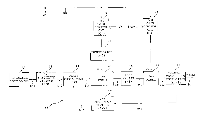
Referring to Fig. 3, description will be made as
regards a PLL type synthesizer according to a first
10 embodiment of this invention. The syn-thesizer is.
similar to that illustrated in Fig~ 1 except for first
and second gain control circuits 41 and 42 each of which
has first and second gains Gl and G2. The first gain
i control circuit 41 is provided on an input line of the
15 modulation signal Sm for the compensator 23. The
compensator 23 has a predetermined transfer function
G(S). On the other hand, the second gain control
circuit 42 is provided on an input line of the
modulation signal Sm for the second adder 22.
A reference frequency signal Sll produced from
the reference oscillator 11 is divided in frequency by
the first frequency divider 12. The first frequency
divider 12 supplies a first divided frequency signal S12
to the phase comparator 14 having a gain K~. The second
25 frequency divider 17 d.ivides the frequency signal Sl.6
and delivers a second divided freq~lency signal S17 to
the phase comparator 14. The phase comparator 14
compares the first divided freq~lency signal S12 with the
~3~3~
second divided frequency signal. S17 and produces a phase
error signal S14 as a comparison result signal.
The modulation signal Sm is supplied to the
first adder 21 through the first gain control circuit 41
5 and the compensator 23 and is added to the phase error
signal S14. The first adder 21 delivers a firs-t
composite signal S21 to the loop filter 15 having a
predetermined transfer function F(S). The loop filter
15 supplies a filtered signal S15 to the second adder
10 22. The modulation signal Sm is also supplied to the
second adder 22 through the second gain control circuit
42 and is added to the filtered signal S15. The second
adder 22 delivers a second composite signal S22 to the
voltage controlled oscillator 16.
The first gain Gl is controlled to be in inverse
proportion to the frequency division ratio N while the
second gain G2 i5 controlled to be in inverse proportion
. to the gain Kv.
: Modulation characteristic of the synthesizer is
20 giv~n by the following equation (1):
Gl~G(S)
S + _ ~ .S.F(S)
D~o(S) = Em(S)~Kv~G2~ , ..... (1)
K~Kv
S ~ .F(S)
where, a~O(s) frequency deviation of the
carrier frequency in the voltage
controlled oscilla-tor 16,
25S: Laplacian operator, and
~ 3 ~ 3 ~
] o
Em(S): input level of the modulation
signal Sm.
Here, .it is assumed tha-t the following equation
(2) is glven:
Gl~G(S) K~.Kv
5- ~S = --, ... t2)
G2 N
the following equation (3) is led:
a~o(S) = Em(S)~Kv~G2 ... (3)
If ~ represents a time constan-t of the
integrator of the compensator 23 and the transfer
10 unction G(S) of the compensator 23 is given by:
G(S) = l/(S~),
equation (2) is rewritten as:
Gl Kv
= _ ... (4)
G2~ K~ N
From equation (4), the following equation (5) is
15 obtained:
Gl = G2~r~X~ Kv/N. ... (5)
If equation (5) is satisfied and if Kv G2 in the
right side of equation (3) is made constant, that is,
the following equation (6) is satisfied:
Kv.G2 = C, ........................ (6)
where C represents a constant, the fre~uency deviation
a~o(S) can be made constant and flat in no relation to
the carrier frequency and the frequency of the
modulation signal Sm.
From equation (6), the following equation (7) is
obtained:
~ 3 ~
11
,
G2 = C/Kv ... (7)
Applying equation (7) to equation (5),
C~K~ ~
Gl = ~ ... (8)
N N
is obtained, where ~ = C-I~K~.
It will be understood from 0quations (7) and (8)
that the object of the invention can be realized by
controlling Gl and G2 in inverse proportion to the
frequency division ratio N and the gain Kv,
respectively. The control is realized by the use of a
10 central processing unit (not shown) known in the art.
That is, the central processing unit controls the gains
Gl and G2 of the first and the second gain control
circuits 41 and 42 to be in inverse proportion to data
of the frequency divi~ion ratio N and the gain Kv input
15 thereto, respeckively.
Referring to Fig. 4, description will proceed to
another aspect of the PLL type synthesizer describe~ in
conjunction with Fig~ 3. The synthesizer i9 similar to
that illustrated in Fig 3 except for the first and the
20 third gain control circuits 41 and 43 each of which has
the first and the third gains Gl and G3 (= G2/Gl).
In the synthestzer, the first gain con-trol
circuit 41 is provided on an input line of the
modulation signal Sm common for the compensator 23 and
25 the second adder 22. The gain Gl is controlled in
inverse proportion to the frequency division ratio N.
On the other hand, the third ~ain control circuit 43 is
i 3 ~
provided on an input line of the modulation signal 5m
for the second adder 22. The gain G3 is controlled in
proportion to the freqllency division ratio N but in
inverse propor-tion to the gain Kv of the voltage
S controlled oscillator 16.
In Fig. 3, input vol-tages Vl ancl V2 to the first
and the second adders 21 and 22 are represented by:
Vl - Em(S)~ G(S)OCl/N
V2 = Emts)G2ocl/Kv
1~ On the other hand, input voltages Vl and V2 in
the circuit in Fig. 4 are given by:
Vl - Em(S)-Gl~G(S)OCl/N
V2 = Em(S~Gl~G3OC(l/N)~(N/Kv3
= Em(S)~G20e1/Kv,
15 because G3 = G2/Gl.
The above-described gain control operati~n is
carried out by a central processing unit described in
conjunction with Fig~ 3. Thus, it is possible to obtain
a constant modulation sensitivity with no use of a
20 variable gain type phase comparator.
Referring to Fig. 5, description will be made as
regards a PLL type synthesizer according to a second
embodiment of this invention. The synthesizer is
similar to that illustrated in Fig. 3 exaept that the
25 second gain control circuit 43 is omitted and that a
fixed gain type voltage controlled oscillator 44 is used
in place of the voltage controlled oscillator 16 shown
in Fiy. 4. This is based on a following reason.
~3~3~
13
I n Fiq . 4, i f the gain Kv of the voltage
controlled oscillator 16 is made constant in no relation
-to the carrier frequency, it i8 possible to make the
second gain G2 constant. In the case, the first gain Gl
5 may only be controlled in inverse proportion to the
frequency division ratio N. Thus, the second gain
control circuit can be omitted by using the fixed gain
type voltage controlled oscilla-tor 44. Such a voltage
controlled oscillator is disclosed in Japanese Published
10 Unexamined Utility Model Application No. 48112/83 (Kôkai
Sho 58-48112 Gou) assigned to the present assignee~
While this invention has thus far been described
in conjunction with preferred embodiments thereof, it
will readily be possible for those skilled in the art to
15 put this invention into practice in various other
manners. For example, the PLL circuit may comprise
o-ther components.