Note: Descriptions are shown in the official language in which they were submitted.
131~
1 217~6-547
BACKGROUND OF THE INVENTION
The present lnvention relates to the production of th:ln
fllm translstors in whlch the conductivlty o~ source and/or ~raln
regions should be hlgh, e.g. for drlvlng llquld crystal dlsplays
(LCD).
Fro~ the prior art lt ls known to produce ~ource and/or
drain regions for a thln Ellm translstor wlth a hlgh conductlvlty,
e.g. greater than or equlvalent to lQ~l cm~l ~y means of lon lm-
plantatlon. Such lon implantation ls cumbersome, re~ulres compll-
cated equlpment and is dl~ficult to apply to relatlvely large sur-
; faces. Further it is known from EP-A-0062079 to produce a seml
conductlon layer ln mlcrocrystalllne form by means of a PECVD re-
actor.
US patent 4625224 relates to a thin film translstor hav-
lng 0.001-5 atomic %CL.
EP-A-0161555 relates to a polycrystalllne sllicon thin
fllm transistor structure havlng source and draln regions ln amor-
phous form.
Also US-A-4,485,121, EP-A-0232619 and GB-A-2156385 show
structures uslng amorphous materlals.
Further the followlng publicatlons are known to the
appllcant: EP-0132076, EP-0200552, EIP-0201270, EP-0206649,
EP-0206650, EP-0228295, EP-0228870, EIP~0229518, EP-0229707,
EP-0232148, EP-0234094, ~P-0240305, ~'P-0240306, EP-0240314,
EP-0241311, EP-0241316, EP-0241317, EP-0242207, ~P-0243074~ and
the artlcle "Very-low-Temperature Slllcon Epltaxy by Plasma-DVD
Uslng SiH4-PH3-H2 Reactants for Blpolar Devlces" from the Japanese
Journ~l of Applled Physics, Vol. 27, No. 4, Aprll 1988~ pages
L493-L495.
SUMMARY OF THE INVENTION
It ls an ob~ect of the present lnventlon to lmprove upon
the above prlor art.
It ls a further ob~ect of the present lnvention to pro-
duce a thln fllm translstor usln~ relatlvely inexpenslve
3~
- . . ,~,.. ..
';- ' .~ ~
,; :
, -2- 13~
equipment.
It is a further ob~ect to produce a thin film
transistor having high conductlvity in source and drain
regions at relatively low temperatures.
s Yet another ob~ect of the present invention is to
produce a thin ~ilm transistor having such a high lateral
conductivity in source and drain regions, that cross
sectional areas of its source and drain contacts can be
smaller than the cross sectional areas of the source and/or
10 drain regions. This feature simplifies alignment in the
production process and is of great importance for reducing
the dimensions of such a thin film transistor.
Another aspect relatss to a depositing process in
which a type of self-alignment is advantageously used.
The present invention relates to a method of
producing a thin film transistor comprising the steps of:
applying a thin film of semiconductor material,
comprising silicon, under such conditions that
20 polycrystalline or microcrystaIline material is formed, onto
a non silicon foundation, e.g. a sheet of glass or quartz;
applying source and/or drain regions of doped
semi-conductor material onto said film;
applying insulating ma~erial onto said film; and
applying a gate region onto said insulating
material;
; ln which the source and/or drain regions are
applied such that the source and/or drain regions have a
crystalline structure that is related to the crystalline
30 structure of said thin film.
Preferably fluor (F) is used in the process, since
F-ions show properties for etching an oxidized top layer.
Further, the presence of F-ions may diminlsh the H content in
a deposited layer which H content could prevent grains from
35 growing.
Further, the present invention relates to a thin
film transistor.
'
:
~ .
--3--
1 3 ~
BRIEF DESCRIPTION O~F THE DRAWINGS
Further ob~ects, features, details and advantag~s
of the present inventlon will be clarified on the basls of
the followlng disclosure in which preferred embodiments are
illustrated wlth reference to the accompanying drawinga, in
5 which:
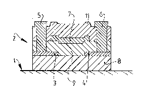
Fig. 1 is a section vlew of a thin film transistor
according to the present invention, produced according to a
method according to the present invention;
Fig. 2 is a graph of the conductivity of the source
10 and drain regions of a thin film transistor of fig. 1,
related to the thickness of the layers applled according to
the invention;
Fig. 3 is a graph of the drain current, related to
the gate voltage of the thin film transistor from fig. l;
Fig. 4 is a graph of the drain current of the thin
film transistor from fig. 1, related to the drain voltage;
Fig. 5 is a graph of the conductivity of the source
and drain regions of the thln film transistor from fig. 1,
produced according to another preferred embodiment of the
20 method according to the present invention;
Fig. 6 a graph showing the conductivity of the
source and drain regions of the thin film transistor from
Fig. 1, produced according to a yet other preferred embodi-
ment of the method according to the present invention; and
Fig. 7A-7C show steps of producing the thin film
transistor of Fig. 1 in accordance with a-method o~ the
invention.
DETAILED DESCRIPTION OF THE PREFERRED_EMBODIMENTS
A thin film transistor 2 disposed onto a sheet or
~:
plate 1 (Fig. 1) of glass or quartz is produced as follows:
A polycrystalline silicon bulk layer or a thin film
8 is disposed in a LPCVD reactor (Low Pressure Chemical
,r~ Vapour Deporsit~i~on) in a direct or indirect way, indirectly
'l35 meaning to ~ dispose an amorphous silicon layer at
550C, after which annealing is executed at 630C, whereby a
grain size up to 400 nm is obtained; it is also possible to
'
~ , .
_4_ 13~ 7
dispose such a polycrystalline layer in a plasrna enhanced CVD
reactor.
Thereafter the polysilicon thin film 8 is dipped in
hydrogen fluoride ~HF-dip), rinsed in a glove box using a N2
5 purge so as to diminish water and oxygen pollution of the
system. It ls apparent that other methods may be used to
prevent water and oxygen pollution.
Next a layer ls disposed under amorphous like or
microcrystalline-like deposition conditions in a PECVD
10 reactor ~Plasma Enhanced Chemical Vapour Deposition); and
then such layer is selectively etched (Auto-Stop-Etching),
such that source and drain regions 3, 4 respectively are
defined.
A gate insulator 9 of SiO2 is then disposed in a
15 APCVD reactor (Atmospheric Pressure Chemlcal Vapour
Deposition); for the skilled artison it is also apparent
that, instead any other gate insulator may be used, such as
silicon nitride. Onto such insulator a metal layer, e.g. of
chromium (Cr~, is disposed, from which after an etching step
20 the gate 7 is produced. The gate may instead be of
semiconductor material.
Next, a covering oxide layer 11 is disposed
over the gate contact and the gate insulating layer 9; and
finally contacts 5, 6 for connecting source, drain and/or
25 gate regions 3, 4, 7 respectively of metal, e.g. aluminium,
~; are disposed after providing holes therefor.
Produclng source and draln regions was executed in
a PD80 deposition system of Plasma Technology under clrcum-
stances according to the following table.
Amorphous- Microcrystalline
like like
Gasflow 1~ PH3 in SiH4 sccm 5-40 3-6
Gasflow H2 sccm 0 150
35 Xf-power W 5-10 30-50
Pressure mTorr 50-100 70
Temperature ~C250-450 250-450
_5_ ~ 3 ~
Test~show that disposing silicon under micro-
crystalline or amorphous conditions produces a
conductivity of such a layer. That is depends on the
conductivity of the underlying layer. The curves of Fiy. 2
5 illustrate this principle. ~urves I and II show the increase
of conductivity at increasing thickness of a layer disposed
on a glass plate, at different grow rates, viz. 3.3 nm per
minute and 1.3 nm per minute, respectively; curves III and IV
show test results under microcrystalline-like diposition
10 conditions in the plasma reactor, having a bulk layer of
polysilicon as foundation, whereby again deposition rates of
3.3, 1.3 nm/minute respectively were used. Dots V and VI show
two separate measurements of a thin layer slowly deposited,
viz. at a rate of 0.12 nm/minute and 0.2 nm/minute
15 respectively. The conductivity or resistance measurements
used a fourpoint probe.
Without limiting the invention, a plausible
explanation of the differences between the curves of Fig. 2
is that epitaxial-like growth is produced and that
20 polycrystalline information of the substrate is transmitted
to the layer to be disposed thereon, whereby an accordingly-
lower resistance of at least a first part of that layer is
produced. The crystalline structure of the upper layer is
related to the crystalline structure of the lower layer.
Typical characteristics ( Figs . 3, 4 respectively)
o~ drain and gate current of a thin film transistor according
to the present invention are satisfactory; curves a, b, c, d
and e ~Fig. 3~ were measured at a drain voltage of 30, 20,
10, 6, 2 volt respectively; curves k, 1, m, n, o and p (Fig.
30 4) at a gate voltage of 40, 35, 30, 25, 20 and 15 volt
respectively.
A second embodiment of the method according to the
invention for producing drain and/or source regions to be
used in a structure shown in Fig. 1, uses amorphous deposit-
35 ion conditions, followed by annealing of the produced layer.
As a standardized preferred embodiment of themethod according to the invention there is used a power of
: - .
:
.
.
-6- ~3~ J
5W, a pressure of 50m Torr, a SiH4 flow of 20 sccm, a
temperature of 300C and 1% PH3 ln the SlH~ flow. For 10
seconds the substrate was dlpped in a 10~ HF solutlon, before
applylng the layer.
An anneallng temperature of 630C for three hours
makes it posslble to produce a thin fllm translstor on Hoya
BSi-glass, whlch remalns solld at such temperature. Fig. 5
shows the achleved conductlvlty C of the source and draln
regions as a function of thickness D.
Line i joins measurlng dots of the conductivlty
layer directly disposed on a glass plate, line f joins
measuring points of such a layer after being annealed, line g
shows the conductivity of a layer of sllicon deposited on a
polycrystalline substrate after a HF dip and line h shows the
15 conductivity after sequential anneallng.
The two triangle~ ln Flg. 5 relate to two measure-
ments on a a-Si:H layer annealed at 600C, deposited on a
sheet of glass and polycrystalllne layer respectively. At
this temperature the difference in conductivity is even more
20 signiflcent, since at 600C less nuclei for crystallization
are formed than at 630C. The value of the conductivity was
found to be independent of the duration of the annealing
process, which duratlon was varied between 1-12 hours. The
thickness of the layer was 20 nm.
~; 25 The reduction in conductivity of the layer at
increasing thickness indicates a decreasing degree of
crystaIline structure of the layer at lncreasing distance
from the polycristaline substrate. A certain minimal duratlon
of the chemical influence of F ions appears to be desired.
Without limiting the invention, an explanation for
further improvement of the conductivity accordlng to the
second embodiment is based on the assumptlon that the source
and/or drain areas forms larger polycrystaline grains spaced
from the substrate, under amorphous-like deposltion
35 conditlons and after anneallng, than at microcrystaline-like
deposition conditions.
1 3 ~ 7
, -7-
The above results were achieved by means of a
relatively simple plasma CVD reactor, which was sealed by
means of 0-rings; no ultra high vacuurn is required; and the
reactor used was relatively inexpensive.
The results of a third embodiment of the method
according to the present invention (Fig. 6) were obtained by
introducing a fluoridized SiH4 gas, or SiHnF~ n (n=1,2,3)
into the PECVD apparatus. Curve rr relates to the position
under microcrystalline conditions, as above mentioned; curve
10 t relates to the preferred embodiment, as above described in
which A-Si:H is annealed; and curve s relates to the third
embodiment, in which SiH2F2 is lntroduced at a rate of 5
sccm, 1% PH3 in SiH4 is introduced at a rate of 1 sccm, H2 is
introduced at a rate of 100 sccm, at a pressure of 3 Torr, a
15 temperature between 250-350 C and an applied power of 17-35
watts.
A fourth embodiment of the method according to the
present invention (Figs. 7A-7C) improves alignment of source
and drain areas relatively to the gate, without using an
20 additional mask step.
By means of a first mask ~not shown) a layer 21 of
polycrystaline silicon was deposited on a quartz she~t 22
(Fig. 7A). By means of a second mask (not shown) a gate
insulator 23 (Fig. 7B) and a gate 24 of conducting or semi-
25 conducting material are provided.
Thereafter source and drain regions 26, 27 resp.~Fig. 7B) were applied in a PECVD reactor under such
conditions that no deposition was measurable onto the quartz
plate 22 nor on the sides of the gate insulator 23. This was
30 achieved by introducing Si~4 into the PECVD reactor in a
temperature range between 300-350 C. At such temperatures
Si-radicals were etched from a SiO2 surface while deposited
on a polysilicon foundation.
Next, by means of two consecutive masks a
35 passivation layer 28 of SiO2 and source and drain contacts
2g, 31 respectively were applied, obtaining a thin film
transistor having mutually aligned gate and source/drain-
, ' ' ~ .:. ' ' :
regions.
Due to the absence of overlap between the gate 24and source and drain regions 26, 27 respectively, the AC
conduction of the thin film transistor is improved; at
5 decreasing dimensions of the process, moreover, the self-
alignment provides distinct advantages over the prior art.
Although the present invention has been described
in connection with a preferred embodiment thereof, many
variations and modifications will now become apparent to
10 those s]cilled in the art. For example,
other epitaxial techniques for depositing onto a
polycrystalline bulk layer can be used; the plasma technlque
using radio frequencies and containing fluor being preferred
due to the possibility of growing at low temperatures and
15 because high concentrations of dopant can be achieved. Other
dopants than phorphos can be included in the process.
Additionally~
source and/or drain regions may further include H,
F, Ge, Cl etc. It is preferred, therefore, that the present
20 invention be limited not by the sp~cific disclosure herein,
but only by the appended claims.