Note: Descriptions are shown in the official language in which they were submitted.
131916q
ELECTRICAL EXCITATION CIRCUIT FOR GAS LASERS
BACKGROUND OF THE INVENTION
This invention relates to electrical pulsing sys-
tems. More particularly, the invention relates to pulsed
electrical power circuits for high repetition rate gas
lasers. Specifically, the invention relates to circuits
in which high power, high voltage, fast rise time, narrow
~ 10 electrical pulses provide electrical energy for exciting
; a gas mixture, thereby producing laser operation.
Electronic transition lasers, such as rare gas
excimer, dimer, and charge transfer lasers, offer scal-
able high energy photon sources in the ultraviolet and
visible wavelengths. These lasers can be scaled to high
pulsed output energies by increasing the volume, pres-
sure, and energy deposition into a high pressure rare gas
halide mixture contained within the laser cavity.
Rare gas halide electronic transition lasers operate
on several fundamental principles. First, an intense
source of electron excitation is used to excite a mixture
of rare gas plus a small percentage of a molecular addi-
tive. A selected rare gas is a dominant component of the
mixture because the electron excitation is initially
deposited into ionization and excitation of the rare gas.
Second, high total pressures are necessary for effective
operation of these lasers. Large volume, self-sustained
glow discharges, however, are extremely difficult to
achieve at high pressures unless special precautions are
taken because high pressure glow discharges tend to
rapidly form an instability and convert to an arc dis-
charge. Arc discharges constrict into small streamers,
thereby eliminating the volume excitation necessary for
proper laser operation. Accordingly, an efficient high
pressure electric discharge for rare gas halide elec-
tronic transition lasers is characterized by a discharge
that is volumetric and stable (i.e., does not degenerate
. ~_
1319169
into a constricted arc). Third, the electron energy in
the discharge should be high enough to produce sufficient
rare gas ions and metastables. There should also be a
sufficiently high current density in order to produce a
sufficient number of excited care gas species in a short
time period which is less than the time required to react
all of the molecular additive. These three criteria
require a high power, high voltage discharge circuit
incorporating some method for stabilizing the discharge
to prevent arcing.
Many problems have been encountered in the implemen-
tation of discharge circuits necessary to produce the
high electron temperatures required in high pressure rare
gas buffered mixtures. Typical problems are that the gas
tends to break down at too low a voltage. Also, dis-
charges at electron energies necessary for efficient
pumping of the laser tend to constrict into an arc unless
the discharge pulse has a very steep rate of rise (under
100 nanoseconds) and the duration is kept shorter than
the arc formation time or the time to react all the mole-
cular additive. The gas after breakdown has a very low
impedance (i.e., less than several ohms~ which necessi-
tates a low impedance discharge circuit for efficient
energy deposition into the laser load. High voltage
charging circuits typically have too large an inductance
to provide either a rapid voltage rise time or a suffi-
ciently low output impedance for optimum energy transfer
to the laser load. Consequently, a key problem associ-
ated with these lasers is the development of an effi-
cient, long-lived, nondestructive, nonablative reliable
and inexpensive method of electron energy deposition into
the laser load. The pulse rise time shaping, pulse width
compression, and impedance matching electrical excitation
circuit of the present invention provides an effective
solution to the problem.
U.S. Patent 4,275,317 discloses a circuit for the
purpose of efficient energy transfer from a relatively
1 3 1 q 1 69
--3--
slow high power, high voltage charging circuit to a laser
load. The circuit comprises one or more saturable
inductor switches, each of which has an associated dis-
tributed capacitance energy storage device. Energy is
provided to a distributed capacitance energy storage
device by a voltage source and is contained therein b~ a
saturable inductor switch. When the energy build-up
reaches a predetermined level, the saturable inductor
switch becomes saturated, thereby allowing the energy to
flow therethrough and into either a next intermediate
capacitance energy storage device or the laser load.
The basic operation of the circuit disclosed in U.S.
Patent 4,275,317 is that of a Melville line. W. S.
Melville, Proceedings of The Institute of Electrical
lS Engineers, Vol. 98, Part III, Number 53, pp. 185-207,
May, 1951. ~ith the aid of Fig. 1, a capacitor Cl is
charged rather slowly by an external charging circuit
with a saturable inductor L1 saturating at the peak
voltage on the capacitor Cl. When the saturable inductor
Ll saturates and switches to a low inductance, a capa-
citor C2 is charged more rapidly to near the same
voltage. A saturable inductor L2 saturates at the peak
voltage on the capacitor C2, charging a small capacitor
C3 in an even shorter time and providing a discharge cur-
rent for the laser load through an inductor LD.
Since the unsaturated inductance is not infinite,some prepulse voltage appears across the laser load of
the circuit disclosed in U.S. Patent 4,275,317. The pur-
pose of the capacitor C3 is to reduce the magnitude of
prepulse to prevent laser breakdown. The prepulse ampli-
tude and voltage rise time are both inversely propor
tional to the value of the capacitor C3. Thus, a
tradeoff between prepulse and rise time occurs. Since
the current does not reverse between charging and
discharging, a magnetic diode across the laser as used in
the present invention would not be practical with the
circuit disclosed in U.S. Patent 4,275,317. The elec-
i 1 3191 6q
-4
trical excitation circuit in accordance with the present
invention reduces the amplitude of the prepulse across
the laser load without an increase in rise time.
When the laser discharge begins, a large fraction of
the discharge current flows from the capacitor C2 through
the saturable inductor L2 of the circuit disclosed in
U.S. Patent 4,275,317. The effective laser discharge
inductance is therefore LD + L2 (saturated). The total
inductance in the discharge loop must be minimized for
optimum laser performance. rrhe inductance of the satur-
able inductor L2 (saturated) will be somewhat above the
air core value and can be as low as a few nanohenries
with careful construction. The discharge loop inductance
(neglecting the inductance of the saturable inductor L2)
is typically a few nanohenries, and, therefore, the
saturable inductor L2 represents a significant increase
in total loop inductance. In accordance with the present
invention, an electrical excitation circuit is provided
which avoids any added inductance in the discharge loop.
U.S. Patent 4,275,317 discloses that distributed
capacitance energy storage devices must be utilized in
order to provide the high voltage, narrow pulses required
by electronic transition lasers. Distributed capacitance
energy storage devices which can be used include coaxial
lines, multiple coaxial lines, parallel plate transmis-
sion lines, or~ two or more parallel-connected capacitors
having an associated natural or added inductance for
creating a pulse shaping network.
U.S. Patent 4,275,317 further discloses that in
order to achieve efficient operation OL the laser, a
pulse shaping network providing less than 10-nanosecond
rise time pulses with durations in the hundred
nanoseconds region must be used, and, therefore, the
saturable inductor switch must have characteristics, and
be constructed, in a manner differing from that of con-
ventional saturable inductor switches. That is, the
saturable inductor switch must be formed of a ~aterial
131ql~q
5--
having a very high permeability and a cross-sectional
thickness on the order of the skin depth of the material
at a frequency corresponding to the desired rise time of
the pulse. For many types of lasers a high voltage
10-nanosecond rise time pulse is desirable, and, there-
fore, the skin depth criterion requires that the material
thickness be on the order of one to two microns. Mag-
netic material films of this thickness can be obtained by
deposition on a plastic insulator backing. These back-
ings can be formed into a tape which is then wound arounda suitable nonmagnetic core material, thereby creating
the saturable inductor switch.
The circuit disclosed in IJ.S. Patent 4,275,317
requires distributed capacitance energy storage devices
and saturable inductor switches which must be tailored
for a specific laser configuration, and are both diffi-
cult to fabricate, and expensive. In accordance with the
present invention, an electrical excitation circuit is
provided which is adjustable for different laser configu-
rations, is largely fabricated with readily availablecommercial components, and is relatively inexpensive.
SUMMARY OF THE INVENTION
The invention provides an electrical excitation cir-
cuit including a pulse forming network for generatingpulses of a given energy level. This network, when
charged, is capable of discharging the charge energy
within a preselected pulse width interval. Charging of
the network is done over a charging period in excess of
the pulse width sought and with a charging current lower
than the pulse discharge current. The slow-charge energy
is rapidly discharged to obtain the high-energy pulse
desired by means of a switching device in the pulse
forming network in the form of a saturable inductor
switch which is not connected in the discharge loop with
the laser load.
131~16q
- ~ -
The invention provides an electrical excitation cir-
cuit which can efficiently produce a high voltage pulse
of very short rise time and duration for a laser load.
The electrical excitation circuit in accordance with the
invention includes a charging circuit means connected in
series with a pulse forming network between a power
source and the laser load. 'rhe pulse forming network
includes at least one capacitor, preferably a discrete
ceramic capacitor, connected to the laser load. A satur-
able inductor switch is connected to the at least onecapacitor so that as the capacitor is chargedr only a
small amount of the energy is absorbed by the saturable
switch until the switch becomes saturated. At that time~
the inductance of the saturable inductor switch
decreases, and the energy contained within the at least
one capacitor is switched into the laser load.
In accordance with the invention, an electrical
excitation circuit for a gas laser is provided connected
between a power source and a laser load comprising:
charging circuit means connected to the power source; and
a pulse forming network connected to the charging circuit
means and the laser load, the pulse forming network com-
prising (a) a saturable inductor switch alternatively
having an unsaturated state and a saturated state, the
saturable inductor switch being shunted across the
charging circuit means and (b) at least one capacitor
shunted across the saturable inductor switch and con-
nected to the laser load, the at least one capacitor
being charged by the charging circuit means when the
saturable inductor switch is in the unsaturated state and
being discharged through the laser load when the satur-
able inductor switch transposes to the saturated state.
The operating point of the saturable inductor switch is
preferably controlled by a bias circl1it, thereby allowing
adjustment of the operating point for a given laser load,
as well as enabling the saturable inductor switch to be
constructed from readily available components. The
1 3 I 9 1 6q
_7
saturable inductor switch is not in the discharge loop of
the laser load. This enables the electrical excitation
circuit to meet the principal requirements for use with
gas lasers, low inductance and ability to switch high
voltage and high currents.
Preferably, the pulse forming network further com-
prises a second capacitor connected between the at least
one capacitor and the laser load and a magnetic diode
charging inductor shunted across the laser load, the
second capacitor being charged by the charging circuit
means through the magnetic diode charging inductor when
the saturable inductor switch is i.n the unsaturated state
and being discharged through the laser load in series
with the at least one capacitor when the saturable
inductor switch transposes to the saturated state. This
effectively provides voltage doubling of the discharge
voltage across the laser load. This capability allows a
lower voltage in the relatively slow charging circuit
means, which simplifies the configuration and reduces
stress on the components. The magnetic diode charging
inductor provides a charging path for the second capa-
citor and at the same time prevents prepulse (breakdown)
of the laser gas. The operating point of the magnetic
diode charging inductor is preferably controlled by a
bias circuit, thereby allowing adjustment of the oper-
ating point for a given laser load, as well as enabling
the magnetic diode charging inductor to be constructed
from readily available components. As in the basic elec-
trical excitation circuit configuration, however, the
saturable inductor switch is not in the discharge loop;
and, also, the magnetic diode charging inductor is like-
wise not in the discharge loop.
In one embodiment of the electrical excitation cir-
cuit of the invention, the charging circuit means
included in the electrical excitation circuit can com-
prise a power source capacitor shunted across the power
source and connected by a series-connected choke and
1 3 1 9 1 6'J
~ .
charging diode to a parallel circuit comprising, as one
branch, a triggerable thyratron and, as the other branch~
a charging capacitor and an inductor, the charging capa-
citor and inductor being in series with the saturable
inductor switch included in the pulse forming network of
the electrical excitation circuit. The at least one
capacitor included in the pulse forming network is
charged when the thyratron is triggered.
In another embodiment of the electrical excitation
circuit of the invention, the charging circuit means
included in the electrical excitation circuit can com-
prise a series-connected choke, primary winding of a
saturable step-up transformer, and power source capacitor
in a parallel circuit with a triggerable silicon con-
trolled rectifier connected across the power source. Theoperating point of the saturable step-up transformer is
preferably controlled by a bias circuit, thereby allowing
adjustment of the operating point for a given laser load,
as well as enabling the saturable step-up transformer to
be constructed from readily available components. A
charging capacitor and a charging diode are connected in
series across the secondary winding of ~he step-up trans-
former, and at least one saturable inductor switch cir-
cuit comprising a capacitor and a saturable inductor
switch is connected between the charging capacitor and
the pulse forming network, the at least one saturable
inductor switch circuit being shunted across the satur-
able inductor switch included in the pulse forming net-
work of the electrical excitation circuit. ~he operating
point of each saturable inductor switch circuit is pre-
ferably controlled by an associated bias circuit, thereby
allowing adjustment of the operating point for a given
laser load, as well as enabling each saturable inductor
switch circuit to be constructed from readily available
components. A plurality of saturable inductor switch
circuits can be cascaded between the charging capacitor
and the pulse forming network, each additional saturable
131ql6q
~ .
inductor switch circuit providing a further degree of
pulse compression and shaping.
A pre-ionization means is preferably included in the
electrical excitation circuit in accordance with the
invention for conditioning the laser gas mixture so that
a uniform discharge occurs across the electrodes of the
laser. Preferably, the pre-ionization means is an x-ray
circuit. Alternatively, a corona pre-ionization circuit
can be included.
Both efficiency and lifetime of a gas laser are
improved by the electrical excitation circuit of the
invention in the laser's electrical discharge system.
The electrical excitation circuit improves the laser's
efficiency by speeding the deposition of electrical
energy into the laser gas. Incorporation of the elec-
trical excitation circuit between the power source and a
gas laser reduces the voltage rise time from hundreds of
nanoseconds, for example, 200 nanoseconds, to tens of
nanoseconds, for example, 30 nanoseconds. This short
rise time is required to produce a uniform (i.e., arc-
less) discharge in the gas, and such a discharge is
required to convert a large portion of the electrical
input to optical output.
BRIEF DESCRIPTION OF THE DRAWINGS
The above and other features of the invention and
the concomitant advantages will be better understood and
appreciated by those skilled in the art in view of the
description of the preferred embodiments given below in
conjunction with the accompanying drawings. In '~he draw-
ings:
Fig. 1 is a schematic diagram of a known pulse
shaping network connected to a charging circuit for
exciting a laser load useful in understanding the fea-
tures and advantages of the electrical excitation circuitin accordance with the invention;
1319169
10 -
Fig. 2 is a schematic diagram of one embodiment of
an electrical excitation circuit in accordance with the
invention for connecting an electrical power source to a
laser load;
Fig. 3 illustrates a B-H curve for the purpose of
facilitating an understanding of the operation of the
saturable magnetic elements included in the circuit of
Fig. 2;
Fig. 4 is a partial scheMatic diagram of another
embodiment of an electrical excitation circuit in accor-
dance with the invention for connecting an electrical
power source to a laser load;
Fig. 5 is a perspective view which shows a preferred
configuration for a saturable magnetic element;
Fig. 6 is a cross-sectional view along line 6-6 of
Fig. 5;
Fig. 7 is a schematic diagram of an x-ray pre-ion
ization circuit preferably included in the circuit of
Fig. 2; and
Fig. 8 is a schematic diagram of a corona pre-ion-
ization circuit alternatively included in the circuit of
Fig. 2.
DESCRIPTION OF THE PREFER~ED EMBODIMENTS
The invention provides a gas laser electrical exci-
tation circuit, that is, a pulse discharge circuit used
to generate a high power, high voltage, high pulse rate,
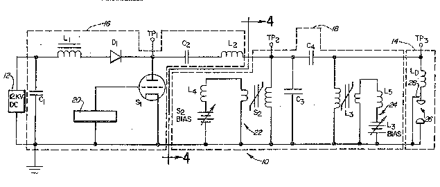
gas laser discharge. Fig. 2 is a simplified schematic
diagram of one embodiment of the electrical excitation
circuit in accordance with the invention, generally indi-
cated by the numeral 10.
Referring now to Fig. 2, the electrical excitation
circuit 10 provides an electrical interface between a
high voltage, high impedance power source 12 and a rela-
tively low impedance laser load 14. The electrical exci-
tation circuit 10 includes a charging circuit 16, which
charges a pulse forming network 18. The pulse forming
1 3 1 ~ 1 6q
i1--
network 18 rapidly releases stored energy to the laser
load 14.
The power source 12 is preferably a direct current
power source. The power source 12, for example, can be a
12 kV direct current rectified power supply.
The charging circuit 16 included in the electrical
excitation circuit 10 shown in Fig. 2 includes a power
source capacitor Cl shunted across the power source 12.
The charging circuit 16 also includes a charging trans~
former or choke Ll and an isolating or charging diode D
connected in series between the power source 12 and a
first terminal or node TPl. The choke Ll and charging
diode Dl isolate the power source 12 from the pulse
forming network 18. A thyratron Sl is included in the
charging circuit 16 connected between the first node TPl
and ground or common, the control electrode of the thyra-
tron being connected to a source of an input trigger
signal generated by a pulse generator circuit 20.
Finally, the charging circuit 16 includes a charging
capacitor C2 series-connected with an inductor L2 between
the first node TPl and a second terminal or node TP2.
The capacitor Cl is significantly larger than the capa-
citor C2.
The pulse forming network 18 included in the elec-
trical excitation circuit 10 shown in Fig. 2 includes asaturable inductor switch S2 connected between the second
node TP2 and common. A biasing circuit 22 for the satur-
able inductor switch S2 is included in the pulse forming
network 18 and comprises a S2 bias power source and a
choke L4 connected in series with the bias winding of the
saturable inductor switch. The S2 bias power source is
an adjustable direct current power supply connected so
that bias current flows through the bias winding of the
saturable inductor switch S2 in the direction from top to
bottom in Fig. 2. The choke L4 provides isolation of the
S2 bias power source from high voltage pulses produced by
transformer action on the bias winding of the saturable
1 3 1 q 1 69
-12-
inductor switch S2. The pulse forming network 18 also
includes a Eirst pulse forming network capacitor C3
shunted across the saturable inductor switch S2. A
second pulse forming network capacitor C4 is included in
the pulse forming network 18 connected between the second
node TP2 and a third terminal or node TP3. Additionally,
the pulse forming networ~ 18 includes a magnetic diode
charging inductor L3 connected between the third node TP3
and common. Finally, the pulse forming network 1~
includes a biasing circuit 24 for the magnetic diode
charging inductor L3, which comprises a L3 bias power
source and a choke L5 connected in series with the bias
winding of the magnetic diode charging inductor. The L3
bias power source is an adjustable direct current power
supply connected so that bias current flows through the
bias winding of the magnetic diode charging inductor L3
in the direction from bottom to top in Fig. 2. The choke
L5 provides isolation of the L3 bias power source from
high voltage pulses produced by transformer action on the
bias winding of the magnetic diode charging inductor L3.
As shown in Fig. 2, the laser load 14 is connected
between the third node TP3 and common. The inductance LD
represents the distributed inductance of the electrode
structure 26 of the laser load 14. A pre-ionization cir-
cuit 28 is preferably included in the laser for condi-
tioning the gas mixture so that there is a uniform
discharge and not arc discharges which constrict to
streamers when the energy stored in the pulse forming
network 18 is released and deposited into the gas mixture
between the electrodes 26.
The electrical excitation circuit 10 performs four
relatively separate operations: a slow resonant charge
of the charging capacitor C2, a medium speed charge of
the pulse forming network 18, an inversion of the voltage
on half of the pulse forming network, and finally the
laser discharge. These operations will be described in
sequence later. The description first treats saturable
` 1 3 1 9 1 69
`1~
magnetic elements, such as the saturable inductor switch
S2 and the magnetic diode charging inductor L3, which are
either in a high inductance (unsaturated) condition or a
low inductance tsaturated) condition as determined by
current flow and bias. The functioning of these satur-
able magnetic elements is described in some detail in
order to facilitate an understanding of the operation of
the electrical excitation circuit 10.
Generally, when a small amount of current is fed
into a saturable inductor, its magnetic permeability, and
hence its impedance, is high. At a certain current
level, however, it saturates; and the permeability and
impedance drop off rapidly, producing a switching effect
so that in the case of a laser, for example, stored
energy is deposited into the laser gas.
A typical B-H curve for ferromagnetic material is
shown in Fig. 3. Several points are plotted on the curve
and will be discussed. First, a brief description of
inductance will be presented.
The inductance of an inductor having a ferromagnetic
core (rather than an air core) is proportional to the
slope of the B-H curve at the operating point
(L a B/ ~ H). When operating in the linear region
(i.e., slope = Ml), this inductance is considerably
greater than the air core value. If the magnetization is
increased to the saturation point (~ BSAT), the slope of
the B-~ curve changes to a lower value (M2) with a corre-
sponding drop in inductance. The magnitude of these
slopes (Ml and M2) and the corresponding inductances
depend upon a number of factors, including the type of
magnetic material and the operating frequency. Gener-
ally, the saturated inductance is between one to two
times the air core value for a properly constructed
saturable inductor.
Operation of a saturable inductor as a switch
requires that the switching action occur at a specific
time after application of voltage. The time required to
1 3 1 9 1 6~
saturate the core can be found from the relationship
NA ~ B
T = E
where N is the number of conductor turns about the core,
A is the cross-sectional area of the core, ~ is the inte-
grated applied voltage, and ~ B is the available change
in magnetization. For maximum flexibility, it is desir-
able to be able to vary the applied voltage E withoutchanging the switching time T. Since the number of turns
N and the area A are fixed for a given core, it is neces-
sary to adjust ~ B.
The value of ~ B for a given material is determined
by the quiescent operating point. Without bias, this
value will be BREM (or RREsET if the core is reset).
It is possible to vary the operating point of the
core to an arbitrary quiescent point (BQ, HQ) by pro-
viding a bias current in the saturable inductor. The
magnitude of the bias current can be found from
1 ~ H
I = N
where l is the length of the magnetic path, N is the
number of turns in the bias winding, and ~ H is the
required change in magnetic field intensity to establish
the quiescent operating point. A variable current supply
can be used to set the operating point anywhere between
+ BS~T. This permits the value of ~ B to be adjusted to
account for different applied voltages, as well as to
allow for tolerances in materials.
Operation of a saturable inductor as a magnetic
diode requires setting the bias point to saturation. ~ny
current in one direction will drive the saturable
inductor further into saturation, resulting in a low
inductance value, while a current reversal will force the
1 3 1 q 1 6q
-15-
saturable inductor into the linear region with a
resulting high inductance value.
The initial phase of operation of the electrical
excitation circuit 10 shown in Fig. 2 is a slow resonant
charge of the charging capacitor C2 included in the
charging circuit 16. The laser discharge sequencing
starts when the 12 kV DC appearing on the capacitor C
from the power source 12 is doubled in a resonant
charging circuit comprising the capacitor Cl, the choke
Ll, the isolating diode Dl, the capacitor C2, the
inductor L2, and the saturable inductor switch S2.
During the 1.2 msec required for the voltage on the capa-
citor C2 to reach 24 kV, the voltage at the second node
TP2 is cla~ped to near zero by the low impedance of the
saturable inductor switch S2 which is biased into a low
inductance (saturated) condition by current flowing from
the S2 bias power source through the choke L4 and the
bias winding of the saturable inductor switch in the
direction from top to bottom in Fig. 2. The sinusoidal
charging current of 1.9 amperes peak also flows through
the saturable inductor switch S2 from top to bottom.
(All currents used are Franklin current not electron cur-
rent, i.e., current flows from plus to minus.) This is
in the same direction as the bias current through the
saturable inductor switch S2 and has negligible effect on
the quiescent magnetic bias point of the saturable
inductor switch. When the voltage at the first node TP
reaches 24 kV, current flow through the choke Ll ceases,
and the isolating diode Dl (being reverse biased) turns
off. The capacitor C2 retains the 24 kV charge until the
thyratron Sl is switched on.
The next phase of operation of the electrical exci-
tation circuit 10 shown in Fig. 2 is a medium speed
charge of the pulse forming network 18. With the capa-
citor C2 charged to 24 kV, the thyratron Sl is thenswitched on by a trigger signal from the pulse generator
circuit 20. The 24 kV charge on the capacitor C2 causes
1 3 1 9 1 6~
~16-
a sinusoidal current of 3200 amperes peak to Elow out of
the capacitor C2. A fraction of the current flows in the
direction from bottom to top in Fig. 2 through the satur-
able inductor swit^h S2 forcing it out of saturation and
into a high inductance (unsaturated) state. The bulk of
the current flows into the capacitor C3 and the series
combination of the magnetic diode charging inductor L3
and the capacitor C4. This charges the capacitors C3 and
C4 to a voltage of approximately 24 kV with negative
polarity on the second node TP2 in one microsecond.
The portion of this current flowing through the mag
netic diode charging inductor L3 produces a prepulse
voltage across the electrodes 26 proportional to the
inductance of the magnetic diode charging inductor. This
prepulse must be held low enough to prevent breakdown of
the laser gas. The magnetic diode charging inductor L3
is magnetically biased into a low inductance (saturated)
state by current flowing from the L3 bias power source
through the choke L5 and the bias winding of the magnetic
diode charging inductor in the direction from bottom to
top in Fig. 2. Furthermore, the current flow from common
toward the third node TP3 during the charging of the
capacitor C4 adds to the bias current which alsu holds
the magnetic diode charging inductor L3 in a low
inductance state. This is adequate to avoid any prepulse
causing a breakdown of the laser gas.
The voltage from common to the second node TP2
increases (as a 1 - cos (wt) function), and at the peak
of the voltage, the saturable inductor switch S2 trans-
poses to a saturated state, that is, saturates in thereverse direction, which allows current to flow through
the saturable inductor switch in the direction from
bottom to top in Fig. 2 in opposition to the bias current
which is swamped out. The time required for the satur
able inductor switch S2 to reverse saturate coincides
with the peak of the voltage and is determined by the
voltage across the saturable inductor switch and the bias
1 3 1 q 1 6q
current through the bias winding of the saturable
inductor switch. Adjustment of this bias current permits
operation over a range of voltages with saturation always
occurring at the peak.
The next phase of operation of the electrical exci-
tation circuit 10 shown in Fig. 2 is the inversion of the
voltage on half of the pulse forming network 18. When
the saturable inductor switch S2 reverse saturates and
switches to a low inductance state, current flows out of
the capacitor C3. A fraction of the current flows back
through the inductor L2 and charges the capacitor C2 to a
low reverse voltage, which aids recovery of the thyratron
Sl. Part of the current attempts to flow through the
capacitor C4 and the magnetic diode charging inductor L3,
which would discharge the capacitor C4 and not produce
laser output. ~owever, this current is opposite to the
bias current through the magnetic diode charging inductor
L3, which causes the magnetic diode charging inductor to
assume a high inductance state. (Saturable inductor L3
- 20 acts as a magnetic diode.) This minimizes the loss of
charge on the capacitor C4. The bulk of the current
through the saturable inductor switch S2 flows from one
terminal of the capacitor C3 to the other, thereby
inverting the voitage across it in 0.1 microsecond.
When the polarity of the voltage across the capa-
citor C3 is inverted, a voltage of nearly 48 kV is
impressed across the electrodes 26. This is adequate to
break down the laser gas so that current flows through
the discharge loop comprising the capacitors C3 and C4
and the distributed inductance LDo
The final phase of operation of the electrical exci-
tation circuit 10 shown in Fig. 2 is the laser discharge.
A fraction of the current from the series combination of
the capacitors C3 and C4 flows through the magnetic diode
charging inductor L3 which is still in a high inductance
state and is lost. As the voltage on the capacitor C3
rings past the peak value, current reverses in the satur-
l ~ l q l 6q
1~-
able inductor switch S2 forcing it out of saturation and
back into a high inductance state, which minimizes the
current lost through the saturable inductor switch. The
bulk of the current flows through the laser gas for
0.1 microsecond, thereby producing a laser pulse.
The voltage rise time is proportional to the
inductance of the discharge circuit switch (saturable
inductor switch S2 saturated). The discharge time is pro-
portional to the inductance of the discharge loop (LD).
Consequently, the electrial excitation circuit 10 has a
fast voltage rise time and a comparable length discharge
time in the load, as is desired in many lasers.
The pulse forming network 18 included in the elec-
trical excitation circuit 10 includes a saturable
inductor switch S2 as opposed to a spark gap or thyratron
switch. The low inductance saturable inductor switch S2
inverts the voltage on the capacitor C3, a function usu-
ally implemented using a spark gap or thyratron switch,
both of which have a relatively high inductance.
Furthermore, the inversion of the voltage on the
capacitor C3 is the result of the sinusoidal current
through the switch which reverses at the peak voltage,
diverting much of the load current through the switch.
Use of the saturable inductor switch S2 rather than a
spark gap avoids loss since the saturable inductor switch
unsaturates when the current reverses, switching to a
high inductance value. This results in a greater frac-
tion of the stored energy being deposited into the laser
load 14.
The saturable inductor switch S2 has additional
advantages over conventional spark gap switches. Advan-
tages include longer lifetime, high pulse rate operation
and simplicity.
The pulse forming network 18 included in the elec-
tricl excitation circuit 10 includes a magnetic diode
charging inductor L3 as opposed to a linear inductor. As
described above, the magnetic diode charging inductor L3
131916~
-19-
is across the laser load 14 to allow charging of the
capacitor C4. The inductance of the magnetic diode
charging inductor L3 must be low enough during charging
of the capacitor C4 to prevent laser gas breakdown (pre-
pulse).
The ideal inductor would have zero inductance duringcharging of the capacitor C4 and infinite inductance
during laser discharge. A low inductance during laser
discharge diverts current from the discharge, reducing
laser efficiency. A single value linear inductor is a
compromise at best between too high and too low an
inductance.
The magnetic diode charginq inductor L3 has the pro-
perty of high inductance when the ferromagnetic material
is unsaturated and low inductance when the material satu-
rates. Typically, there is a ratio of 100:1 between high
and low inductance. The current reversal in the magnetic
diode charging inductor L3 between charging of the capa-
citor C4 and laser discharge drives the magnetic diode
charging inductor from a saturated (low inductance) state
to an unsaturated (high inductance) state, thereby
approximating an ideal inductor.
In another embodiment of the electrical excitation
circuit in accordance with the invention, a cascaded mag-
netic charging circuit 30 shown in Fig. 4 replaces thecharging circuit 16 described above in conjunction with
Fig. 2. Referring to Fig. 4, the cascaded magnetic
charging circuit 30 is connected to a power source 12'.
The power source 12' is a relatively low voltage power
supply compared with the power source 12 described in
conjunction with Fig. 2. The power source 12', for
example, can be a 1 kV direct current rectified power
supply.
The cascaded magnetic charging circuit 30 shown in
Fi~. 4 also includes a charging transformer or choke Ll',
the primary winding of a saturable step-up transformer
XFMRl, and a power source capacitor Cl' connected in
1 3 1 ~ 1 6~
-20-
series between the power source 12' and common. The
saturable step-up transformer XFMRl, for example, can be
a 1:25 transformer. The cascaded magnetic charging cir-
cuit 30 additionally includes a biasing circuit 31 for
the saturable step-up transformer XFMRl, which comprises
an XFMRl bias power source and a choke L6 connected in
series with the bias winding of the saturable step-up
transformer. The XFMRl bias power source is an adjust-
able direct current power supply connected so that bias
current flows through the bias winding of the saturable
step-up transformer XFMRl in the direction from bottom to
top in Fig. 4. The choke L6 provides isolation of the
XFMRl bias power source from high voltage pulses produced
by transformer action on the bias winding of the satur-
able step-up transformer XFMRl. A silicon controlled
rectifier SCRl included in the cascaded magnetic charging
circuit 30 is shunted across the choke Ll', the primary
winding of the saturable step-up transformer XFMRl, and
the capacitor Cl'~ the gate of the silicon controlled
rectifier being connected to a source of an input trigger
signal generated by a pulse generator circuit 20'.
The cascaded magnetic charging circuit 30 further
includes a capacitor C2' connected between the secondary
winding of the saturable step-up transformer XFMRl and a
first terminal or node TPl'. An isolating or charging
diode Dl' included in the cascaded magnetic charging cir-
cuit 30 is connected between the first node TPl' and
common.
The cascaded magnetic charging circuit 30 finally
includes at least one saturable inductor switch circuit
32, such as a saturable inductor switch circuit 34, com-
prising a capacitor C5 connected between t~e first node
TPl' and common, as well as a saturable inductor switch
S3 connected between the first node TPl' and the second
node TP2 which corresponds to the second node TP2 shown
in Fig. 2. The saturable inductor switch circuit 34 also
preferably comprises a biasing circuit 35 for the satur-
1319169
- ~1
able inductor switch S3, which comprises a S3 bias power
source and a choke L7 connected in series with the bias
winding of the saturable inductor switch. The S3 bias
power source is an adjustable direct current power supply
connected so that bias current flows through the bias
winding of the saturable inductor switch S3 in the direc-
tion from left to right in Fig. 4. The choke L7 provides
isolation of the S3 bias power source from high voltage
pulses produced by transformer action on the bias winding
of the saturable inductor switch S3.
Referring to Fig. 4, a second saturable inductor
switch circuit 36 is shown comprising a capacitor C6 con-
nected between the saturable inductor switch S3 and
common, as well as a saturable inductor switch S4 con-
nected between the saturable inductor switch S3 and thesecond node TP2. The saturable inductor switch circuit
36 also preferably comprises a biasing circuit 37 for the
saturable inductor switch S4, which comprises a S4 bias
power source and a choke L8 connected in series with the
bias winding of the saturable inductor switch. The S4
bias power source is an adjustable direct current power
supply connected so that bias current flows through the
bias winding of the saturable inductor switch S4 in the
direction from left to right in Fig. 4. The choke L8
provides isolation of the S4 bias power source from high
voltage pulses produced by transformer action on the bias
winding of the saturable inductor switch S4.
The various saturable inductor switch circuits 32
are cascaded to gradually narrow and sharpen the pulse
fed to the pulse forming network 18 shown in Fig. 2.
Each saturable inductor switch, S3, S4, etc., shown in
Fig. 4 is used as a "hold off" device. After a "hold
off" period elapses, that is, the saturable inductor
switch saturates, the discharge current from the associ-
ated capacitor, C5, C6, etc., respectively, flows asthough the ~aturable inductor were no longer there, and
the capacitor in the following saturable inductor switch
1 3 1 9 1 6q
-~2-
circuit 32 is charged. The output of the last saturable
inductor switch circuit 32 is connected between the
second node TP2 and common.
The power source 12' and cascaded magnetic charging
circuit 30 shown in Fig. 4 can be substituted for the
power source 12 and the charging circuit 16 shown in
Fig. 2. Considered in more detail, the electrical exci
tation circuit 10 shown in Fig. 2 is broken along line
4-4. The power source 12 and the charging circuit 16 are
disconnected. The output of the last saturable inductor
switch circuit 32 shown in Fig. 4 is then connected in
shunt across the saturable inductor switch S2 shown in
Fig. 2 in order to accomplish the substitution.
The inclusion of the cascaded magnetic charging cir-
cuit 30 provides an electrical excitation circuit 10 inwhich no spark gaps or thyratron switches are included.
That is, the electrical excitation circuit 10 includes
only a silicon controlled rectifier SCRl and saturable
inductors as switches and therefore has an extended life-
time. Furthermore, the saturable step-up transformer
XFMRl provides isolation of the relatively low voltage
power source 12' from the high voltages elsewhere in the
electrical excitation circuit 10.
In the first phase of operation of the electrical
excitation circuit 10 which includes the cascaded mag-
netic charging circuit 30 shown in Fig. 4, the power
source capacitor Cl' is charged from the 1 kV power
source 12' through the choke Ll' and the primary winding
of the saturable step-up transformer XFMRl by current
flowing through the primary winding in the direction from
top to bottom in Fig. 4. The primary and secondary wind-
ings of the saturable step-up transformer XFMRl are con-
figured so that the direction of current flowing in the
secondary winding is opposite to that in the primary -
winding. The charging diode Dl' blocks any significantcharging of the charging capacitor C2' during the
charging of the power source capacitor Cl'.
131ql6q
-23-
After the power source capacitor Cl' is fully
charged, the pulse generator circuit 20' produces a
trigger signal which fires the silicon controlled recti-
fier SCRl. Current 10ws out of the power source capa-
citor Cl' through the primary winding of the saturablestep-up transformer XFMRl in the direction from bottom to
top in Fig. 4. The current flowing through the primary
winding of the saturable step-up transformer XFMRl
induces a voltage across the secondary winding of the
saturable step-up transformer which causes a current to
flow through the secondary winding in the direction from
bottom to top in Fig. 4, as well as through the charging
capacitor C2' and charging diode Dl'. The discharge of
the power source capacitor Cl' takes 60 microseconds
adjusted by the level of the bias current flowing through
th bias winding of the saturable step-up transformer
XFMRl, at the end of which time the charging capacitor
C2' is charged to a peak voltage of 25 kV.
When the voltage on the charging capacitor C2'
reaches the peak voltage, the saturable step-up trans-
former XFMRl saturates. Consequently, the charging capa-
citor C2' discharges through the secondary winding of the
saturable step-up transformer XFMRl and charges the capa-
citor C5 included in the initial saturable inductor
switch circuit ~4 with negative polarity on the first
node TPl'. As adjusted by the level of the bias current
flowing through the bias winding of the saturable ind-
cutor S3, at the peak of the voltage on the capacitor C5,
the saturable inductor switch S3 included in the satur-
able inductor switch circuit 34 saturates, thereby trans-
ferring the voltage on the capacitor C5 to the capacitor
C6 included in the next saturable inductor switch circuit
36. Similarly, as adjusted by the level of the bias cur-
rent flowing through the bias winding of the saturable
inductor S4, at the peak of the voltage on the capacitor
C6, the saturable inductor switch S4 included in the
saturable inductor switch circuit 36 saturates, thereby
1 3 1 q 1 69
--~4~
transferring the voltage on the capacitor C6 to the pulse
forming network 18 shown in Fig. 2.
Each cascaded saturable inductor switch circuit 32
shown in Fig. 4 provides pulse rise time sharpening and
pulse width compression. The pulse width of the voltage
transferred from the capacitor C6 to the pulse forming
network 18 shown in Fig. 2, for example, is 800
nanoseconds as compared to the 60-microsecond pulse width
of the voltage transferred to the charging capacitor C2'
shown in Fig. 4. The pulse forming network 18 shown in
Fig. 2 operates in the manner described earlier for
imparting electrical energy to the laser load 14.
By way of example, the electrical excitation circuit
10 shown in Fig. 2 was adapted for exciting a xenon chlo-
ride excimer laser load. Referring to Fig. 2, the valuesand types for the various circuit elements were selected
as shown in Table I.
TABLE I
Cl 4.7 microfarads
Ll 3.0 henries
Dl SlKW48KA4
Sl HY-5
C2 60 nanofarads
L2 21 microhenries
S2 1.9 microhenries (unsaturated)
C3, C4 32 nanofarads
L3 60 microhenries (unsaturated)
4, 5 100 microhenries
As an alternative, the cascaded magnetic charging circuit
30 shown in Fig. 4 was substituted for the charging cir-
cuit 16 shown in Fig. 2, in which case the values and
types for the various circuit elements were selected as
shown in Table II.
1319169
--25-
TABLE II
SCRl T7SHl64624DN
L1' 10 microhenries
XFM~ 25 step-up,
410 microhenries (saturated)
C1' 40 microfarads
C2 ~ C5, C6 60 nanofarads
Dl SlKW48KA4
S3 30 microhenries (saturated)
s4 1.5 microhenries (saturated)
S2 1.9 microhenries (unsaturated)
C3, C4 32 nanofarads
L3 60 microhenries (unsaturated)
L4, L5 100 microhenries
L6~ L7~ L8 150 microhenries
The capacitors are preferably discrete ceramic capa-
citors. However, water line capacitors can be used,
although high voltage arcs and corrosion can occur in
water line capacitors.
The saturable inductor switch S2 and the magnetic
diode charging inductor L3 shown in Fig. 2 can be struc-
tured as illustrated in Fig. 5 and include an inductance
element 38 which surrounds a nonconductive tube 40 sup-
ported by a housing 42. The nonconductive tube 40 is
constructed from insulative material, such as polyvinyl-
chloride. The housing 42 can contain the remainder of
the circuit elements of the pulse forming network 18
shown in Fig. 2 and is constructed from insulative
material, such as polyvinylchloride. Bias current flows
through a conductor 44 which is disposed in the interior
of the nonconductive tube 40 as shown in Fig. 5.
Fig. 6 is a cross-sectional view along the line 6-6
shown in Fig. 5 and illustrates the structure of the
inductance element 3~ in greater detail. The inductance
element 38 includes a plurality of cores 46 contained
131q16q
-26-
within an outer length of copper tubing 48. There can
be, for example, 24 cores, such as 3C8 Ferroxcube cores
included in the inductance element 38. A sheet of insu-
lative material 50, such as polypropylene sheet, is
wrapped around the cores 46. KAPTON tape insulation is
preferably applied to the end core 46, as indicated gen-
erally by the numeral 52. An inner length of copper
tubing 54 ~ies between the cores 46, which are wrapped
with the insulative material 50, and the nonconductive
tube 40. The outer copper tubing 48 is connected to the
inner copper tubing 54 at one end (i.e., the left end in
Fig. 6~. The outer copper tubing 48 is connected at the
other end (i.e., the right end in Fig. 6) to one of the
nodes TP2 or TP3 of the pulse forming network 18 shown in
Fig. 2. The inner copper tubing 54 is connected at the
other end (i.e., the right end in Fig. 6) to common.
The bias winding in Fig. 6 is illustrated as a
single turn bias supply conductor 44. The saturable
inductor switches S3 and S4 shown in Fig. 4 can also be
structured as shown in Figs. 5 and 6.
The electrical excitation circuit 10 as indicated
earlier preferably includes a pre-ionization means 2~ for
conditioning the laser gas as shown in Fig. 2. The pre-
ionization means is preferably an x-ray circuit as illus-
trated in Fig. 7. The x-ray circuit comprises a length
of anodized aluminum tubing 6~ plated on the interior
with a layer of gold, indicated by the numeral 62, as the
anode, and carbon felt 64 as the cathode. A high volta~e
pulsed power source ~6 is connected across the anode and
cathode for producing x-rays which ionize the laser gas
between the electrodes 26. The aluminum tubing 60 is
evacuated to a pressure of 5 x 10 6 mm Hg during opera-
tion.
Alternatively, the pre-ionization means 28 shown in
Fig. 2 can be a corona pre-ionization circuit as illus-
trated in Fig. 8. The corona pre-ionization circuit com-
prises a corona element 68, which is formed by an insu-
* trade mark.
~, `
1 3 1 9 1 69
27-
lated conductor contained within a quartz tube, disposed
near the uppermost of the electrodes 26, as well as an
insulated conductor 70, which connects the conductor
within the corona element 68 to common. The corona pre-
ionization circuit does not require an additional powersource.
A laser incorporating an electrical excitation cir-
cuit as provided by the present invention has many advan-
tages over conventional pulse shaping networks which
include switches such as multichannel arc switches (rail
gaps), thyratrons, spark gaps, or ignitrons. The elec-
trical excitation circuit according to the present inven-
tion can be operated at high repetition rates and at high
powers and voltages and will have a very long lifetime
compared with conventional laser discharge circuits.
Although the invention has been described and illus-
trated in detail, it is to be clearly understood that the
same is by way of illustration and example only and is
not to be taken by way of limitation. Consequently, the
spirit and scope of this invention are ascertainable only
by reference to the appended claims.
3~