Note: Descriptions are shown in the official language in which they were submitted.
~ 3 2 ~ 3
1 Backqround of the Inv~ntion
This invention relates generally to digital
data processing systems, and, in particular, to a bus
structure suitable for use with multiprocessor
computer systems.
Multiprocessor computer systems prov;de
multiple independent central processing units (CPUs)
which can be coherently interconnected. Recent
efforts in the multiprocessor field haYe concentrated
on multiprocessor systems wherein each of a plurality
of processors is equipped with a dedicated random
access or cache memory unit. These multiple
processors typically communicate with one another via
a common system bus structure ~iOe. shared bus
systems), or by signalling with;n a shared memory
address area ~i.e. shared address space systems).
In recent years, a wide range of structures
and methods have been proposed or developed to
interconnect the processors of a shared bus system
multiprocessor~
.
One such shared bus muLtiprocessing computer
syst~m is disclosed in United Kingdom Patent
Applicati~n ~o. 2,1~8,205 ~publishsd February 4,
19~7). Th~t sy~tem is understood to comprise a
plurality of processors, each havin~ its own
dedica~ed cache memory, and wherein the cache
memories are connected to one another over a shared
bus.
'.
~320~03
1 Convention~l shared bus systems, how~ver,
lack adequate bandwidth to provide multiple
processors with short effective access times during
periods of high bus contention. Although a number of
caching schemes have been proposed and developed for
the purpo~e of reducing bus contention, bus
saturation still limits the speed and size of
multiprocessor computers.
Additionally, the speed of a conventional
bus structure i5 limited by the speed of light and by
bus length. In particular, as morQ processors are
linked to a conventional bus, bus length incraases
and thus the time required for signal transfer
increases.
Another class of interconnection systems,
known as crossbar networks, avoid some of the
limitations of conventional bus syst*ms. In a
crossbar network, however, the path taken by a given
~ignal cannot be uniquely specified. Moreover, cost
increases as the s~uare of the number of
interconnected processors. The!;e characteristics
make crossbar networks unsuitab:Le or multiprocessor
systems.
There accordingly e~ists a need for an
interconne~tion system for multiprocessor computer
systems which ~an accommodate the lar~e volume of
interconnect access request~ generated by multiple
processor~. In particular~ there e~ists a need for
an interconnection system in which transfer speed i~
independent o~ the number of interconnected
processors.
, - . ,
_3_
1 It is thus an object of the invention to
provide an improved multiprocessor digital data
processing system.
It is ano~her object of the invention to
provide an interconnection system for ~
multiprocessor digital computer structure which can
provide multiple processors with short effective
access times under all operating conditions.
It is yet another object of the invention to
provide an interconnection system having the above
characteristics which is applicable to both shared
memory an~ non-shared memory multiprocessors.
It is a further object of the invention to
provide an interconnection system having high
bandwidth and the capability of transferring signals
at rates sufficient to 3110w multiprocessors to
operate at full speed.
It is another object of. the invention to
provide an interconnection system for a
multiprocessor wherein bandwidth increases in
: 25 proportion to the number of processors.
It is a further object of the invention to
provide an interconnection system wherein transfer
speed is independent of the number of interconnected
processors, and is limited only by the switching
speed o$ an individual interconnect~
. ~,
-4_ ~ 32~3
1 Other general and specific objects of the
invention will in part be obvious and will in part
appear hereinaf~er.
: :
.. . .
'' : , - ~
-5~ 3
1 Summary of the Invention
The aforementioned objects are attained by
the invention, which provides a digital data
processing apparatus haYing a bus structure for
transferring information-representative digital
signals, the bus structure inclu~ing a shi~t register
element having a set of digital storage and transf~r
stages connected in series, for se~uentially storing
and transf~rring said information-representative
digital signals. The invention also includes a
plurality of processing cells, connected in a ring
configuration to the bus structure, wherein at least
one of the cells includes a central process;ng unit,
an associated memory element for storing
information-representative digital signals, coupled
with the central processing unit for information
transfer therebetween, and associated cell
interconnect units, connected in circuit with the
shift register element, and with an associated
central processing unit, for transferring
information-repxesentative si~nals onto the shift
register element.
In accordanc~ with one aspect of the
invention, the bus structure comprises unidirectional
information-representative signal flow paths, and the
cell interconnect units include elements ~or driving
inormatio~-representative ~ignals alon~ the flow
path define~ by the bus structure.
' . ':: - , ' , . ,
.
: ~, ' .
-6- 132~3
1 In another aspect of the invention, each
stage of the shift register element includes latch
and register elements for storin~ a digital
information-representative signal word of (n) digital
bits, where ~n) is a posit;ve integer, ~nd the cell
interconnect units include timing control elements
respons~ve to applied digital clock cycle signals for
sequentially driving information-representative
digital words through successive stages of the shift
register element at a rate controlled by the digital
clock cycle rate. In accordance with this aspect of
the invention, the shift register element includes.
elements for storing in a giv~n sta~e of the shift
register element a g;ven digital word for one applied
digital clock cycle, and transferring a given digital
word to a succeeding stage of the shift register
element after an applied digital clock cycle.
Moreover, in this aspect of the invention, each cell
interconnect unit has associated therewith a subset
of ~s~ ~tages of the shift register strueture, where
(s) is a positive integer, so that a given digital
word is resident in a stage associated with each cell
interconnect unit for ~s~ applied digital clock
cycles.
In another àsp~ct of the invention, the
6hift regi~ter structure includes eleme~ts for
se~uentially transferring digital signal pa~kets
comprising ~w) correspond;ng digital words, where ~w~
i~ a positive integer, so that a digital word
correspo~din~ to a given digital signal packet is
resident in at least one stage a~sociated with a
given cel~l interconnect unit or ~s) X (w) digital
cl~ ycl~s.
-
-7- ~ 3 ~ 3
The invention f~rther provides data
processing apparatus wherein the shift register
structure includes elements for simultaneously
transferring to successive shift register stages ~p)
digital signal packets, where ~p) ;s a positive
integer giYen by
(p) = ~c) (s~w)
where (c) is the nurnber of cell interconnect units,
(s) is the number of shift register stages associated
with each cell interconnect unit and (w~ is the
number of digital words in each digital signal
packet. In accordance with the invention, as the
number of cell interconnect units in a ring is
increased, the flux of transfer operat;ons through
the ring is constant, and the number of bus
operations which can be executed during a completP
bus cycle increases linearly.
Another aspect of the invention provide~
data processing apparatus whersiLn at least one of the
processing cells described above~ includes elements
for generating and transmitting to an associated cell
interconnect unit a cell interconnect ~ontrol signal
repreæentative of a re~ues~ to stor~ an
information-r~presentative signal in a first
associated stage of the shift register structure,
In accordance with this aspect o~ the
inYention, at least one of the processing cells
i~cludes elements for ~enerating and transmitting to
.
.: .
.
'. . ,- ' ' ,
32~0~3
an associated cell interconnect unit a cell
interconnect control signal representative of a
request for access to an information representative
signal stored in a irst associated stage of the
shift register structure. The associated cell
interconnect unit in ~urn includes elementsO
responsive to the cell interconnect control signal,
for extracting the information-representative signal
stored in the first associated sta~e of the shift
register structure and for transferring the extracted
information-representative signal to the associated
cell.
In a digital data processing apparatus of
the type described above, the associated cell
interconnect unit can also include an element,
responsive to the cell interconnect control signal,
for replicating the information-representative signal
stored in the first associated stage of the shift
register structure and for transferrinq the
replicated information-representative signal to the
cell.
In yet another aspect of the invention, at
least one of the processing cells includes an element
for ge`nerating and transmitting to an associated cell
interconn~Gt unit, a cell interconnect control signal
representative of a re~uest to transf~r, unchanged,
an information representative signal stored in a
first associated stage of the shift register
structure to a second, succeeding associated s~age of
the shift register structure.
~5
-9- ~32~3
1 In accordance with this aspect of the
invention, the associated cell interconnect unit can
;nclude an element, responsive to the cell
interconnect control signal, for ~nabling transfer to
S the second, succeeding associated stage of the shift
register structure the information-representative
signal stored in the first associated stage of the
shift register structure.
The invention further contemplates data
processing apparatus of the type described above,
wherein at least one of the processing cells include
an element for generating and transmitting to an
associated cell interconnect means a cell
interconnect control signal representative of a
request to identify a given digital word stored in an
associatecl stage of the shi f t register structure as
the first word of a data packet. In accordance with
this aspect of the invention, the associated cell
interconnect unit can include means, responsive to
the cell interconnect control s;gnal, for setting a
portion of the given digital word to a selected value
identifying the given digital word as the first word
of the data packetO
Yet ano her aspect of the invention provides
a di~ital data processing apparatus having a bus
structure and plurality of processing cells of the
type described above, whaxein at least one o~ the
cell~ includes an associated cell interconnect unit,
connected in circuit with the shift register
structure, and with an associated central processing
unit, or transferrin9 information-representative
1320~3
signals onto the shift reyist~r structure, the cell
interconnect unit comprising a sub~et of serially
connec~ed ~tages of the shift register struc~ure.
Accordingly, in one of i~s emb~diments, the
present invention relates to a digital data proce3sing
apparatus comprising
A. bus means for transferring packets of
information-representative digital signals, said bus
means including shift register means comprising a
plurality of digital storage and transfer stages
connected in series in a ring configuration for
sequentially storing and transferring said
information-representative digital signals, wherein
each said stage within said shit register means
includes means for storing an information-
representative signal of (M) bits, where (M) is
greater than one,
B. a plurality of processing cells,
connected in a ring configuration through said bus
means, each processing cell being in communication
with an associated subset of (N) said stages, where
~N) is greater than one, at least one of said cells
having associated memory means coupled thereto for
storing a plurality of information-representatiYe
digital signals,
C. said at least one said processing cell
further including cell interconnect means, conne~ted
to said associated subset of stages and said
associated memory means, for selectively transferring
information-representative signals between said
associated subset of stages and said associated
memory means,
D. said cell interconnect means including
means or performing.at least one of modifying,
e~tracting, replicating and transferring a packet of
~,
-lOa-
~32~0~3
digital information-representative signals, wherein
at least a portion of said packet is stored within
said associated subset of stages, based on an
association, if any, between an information-
representative signal identified in that packet andone or more information-representative signals of
said plurality of information-representative signals
stored in said associated memory means, and
E. said cell interconnect means including
means responsive to applied digital clock cycle
signals for simultaneously transferring at least a
selected digital signal packet through successive
sta~es of said associated subset of stages, at a rate
responsive to said digital clock cycle rate, while
performing said at least one modifying, e~tracting,
replicating and transferring operation on that same
digital signal packet.
In a further embodiment, the present invention
relates to a digital data processing apparatus comprising
A. bus means for trans~Eerring packets of
information-representative digital signals, said bus
means including shift register rneans comprising a
plurality of digital storage and transfer stages
connected in series in a ring configuration for
se~uentially storing and transferring said
in~ormation-representative digital sign~ls, wherein
each said stage within said shift register means
includes means for storing an information-
representative signal of ~M) bits, where (M) is
greater than one,
B. a plurality of processing cells,
connected in a ring configuration through said bus
means, each processing cell being in co~nunication
with an associated subset o (N) said stages, where
(N) is greater than one, at least one of said cells
having associated memory means coupled thereto for
storing information-representative digital signals,
`B
~32~3
-lOh-
1 C. said at least one said proces~sin~ cell
further including cell interconnect means, connected to
said associated subset of stages and said associated
memory means, for selectively transferring inEormation-
representative signals between said associated subset of
stages and said associated memory means, and
D. said cell interconnect means including means
responsive to applied digital clock cycle signals for
simultaneously transferring at least a selected digital
signal packet thro~gh successive stages of said associated
subset of stages, at a rate responsive to said digital
clock cycle rate, while performing at subset o~ stages, at
a rate responsive to said digital clock signals, while
performing said at least one modifying, extracting,
replicating and transferring operation on said digital
signal packet.
In another aspect ~he invention resides in a
method of operating a digital data processing apparatus
comprising
A. providing a plurality of processing cells, at
least a selected one of which includes an associated
memory element for storing a plurality of information-
representative digital signals,
BD transferring packets of information-
representative digital signals between said processing
cells on a bus comprising a plurality of digital storage
and transfer stages connected in series in a ring
configuration, wherein each said storage and transfer
stage stores an information representative signal o~ (M~
bits, where (M) is greater than one, and wherein each
processing cell is in communication with an associated
subset oE tN) said stages, where (N) is greater than one,
~i`'
-lOc- ~2~3
l C. selectively transferring information-
representative signals between said memory element and the
subset of stages associated with said selected processing
cell,
D. responding to an association~ if any, between
i) an information-representative signal
identified in a selected packet of digital
information-representative signals at least a
portion of which packet is stored within the
IO subset of sta~es associated with said selected
processing cell, and
ii) one or more information-representative
signals stored in the memory element associated
with that processing cell, to selectively perform
at least one of a mod.i~ying/ extracting,
replicating and transferring operation on that
packet of digital information~representative
signals,
E. performing said at least one modifying,
extracting, replicating and transferring operation on said
selected packet of digital information-representative
signals while simultaneously transerring, at a rate
responsive to applied digital clock cycle signals, that
packet through the successive stages associated with said
selected processing cell.
The invention accordingly comprises an apparatus
and method embodying eatures of constructionr
combinations of elements and arrangements of parts as
exemplified in the following detailed disclosure, and the
l~ scope o the invention is indicated in the claims.
~"~
32Q~Q3
1 ~rie Description of the Drawi~~
For a fuller understanding of the nature and
objects of the invention, reference should be mad~ to
the following detailed description and the
accompanying drawings~ in which:
FIGURE 1 depicts the structure of a
multiprocessor computer system constructed in
accordance with the invention
FIGURE 2 depicts detail of the structure of
a processing cell illustrated in FIGURE 19
FIGURE 3 depicts a plurality of the
processing cells of FIGURE 2 interconnected by a bus
system constructed in accordance with the invention;
FIGURE 4 depicts detail of the structure of
a cell interconnect of FIGURE 3;
FIGURE 5 depicts detail of the ~tructure of
a cell interconnect unit in the ~ell interconnect of
FIGUR~ 4;
,
FIGURE 6 depîcts the shift registe~ stages
associated with the cell interconnect~ of FIGURE 3;
FI~URE 7 depict~ clnck ~ignal distribution
in the embodiment o~ FI~URE 3; and
FIGVRE 8 depicts the contents of an
exemplary data packet processed by the embodiment of
FIGURE 3.
D
~L32~3
- 1 1 a -
1 FIGURES 9A and 9B depict a cell interconnect
schematic.
FIGURES 10A to 10G depict a cell interconnect unit
directory schematic.
FIGURES 11A to 11C depict a cell interconnect unit
cache group.
FIGURES 12A and 12B depict a cell interconnect
unlt datapath schematic.
FIGURES 13A to 13D depict a cell interconnect
datapath cell schematic.
FIGURES 14A and 14B depict datapath cache group
low schematic.
FIGURES 15A and 15B depict a datapath cache group
high schematic.
FIUGRES 16A to 16C depict a cell interconnect unit
datapath extract FIFO schematic.
FIGURES 17A to 17E depict a datapath insert FIFO
schematic.
FIGURES 18A to 18E depict ideal cell interconnect
unit cloc k d iagrams.
-12- ~32~3
1 DescriptiQn of th~ Illustrated Emhodiment
Str~cture
FIGURE 1 depicts a multiprocessor computer
utilizing a bus system constructe~ in accordance with
the invention. The multiprocessor system is
hierarchically constructed from processors, cells and
domains. Each of the processing cells 0, 1, 2 and 3
contains a pr~cessor and cache memory, as discussed
below in connection with Figure 2. The cells 0-3 are
interconnected by cell interconnects (CIs~ 10-13 and
bus 8, thereby collectively forming Domain 0.
Domains, in turn, are interconnected by domain
interconnects ~not shown), to form a complete
system. The structure of cell interconnects is
described hereinafter in connection with FIGURES 4
and 5, and the structure and operation of the
illustrated multiprocessor system is more fully
discus~ed in Can~dian Patent Application No. 582,560,
filed on even date herewith.
FIGURE 2 depicts the components of
processing cell 0, including processor (PROC) 50,
cache 40 and cell interconnect (CI) 10. Data,
parity, and control signals passed between processor
50, cache 40 a~d cell interconnect 10 are indicated
in F~URE 2. The datapath width associated with each
respective signal is in~icated by numera~s in
brackets~ For esample, cach~ data ~ignals
~cache_data t64]) passed between cell int rconnect 10
and cache 40 hav~ a 64 bit datapath width, as do
processor ~ata signals (p~data~64J~ passed between
cache 40 and processor 50.
~3
-13- ~3~
1 As FIGURE 2 illustrates, cell interconnect
10 receives and transmits DOMAIN DATA ~ignals
(dmn_data), DOMAIN PARITY signals dmn_parity), DOMAIN
EMPTY signals (dmn_empty), DOMAIN HEADER signals
(dmn_hdr), DOMAIN CELL ADDRESS signals
(dmn_cell_addr), and DOM~IN CLOCK signals (dmn_clkSOj
discussed in greater detail hereinafter. In
addition, cell interconnect 10 processes cache
arbitration, routing, operation, and parity signals
as indicated in FIGURE 2. The structure of cell
interconnect 10 is discussed in greater detail below
;n connection with FIGURE 4. Moreover, urther
understanding of the logic components and structure
of cache 40 and processor 50 may be had by reference
1~ to Figures 9 to 18, and by reference to Canadian Patent
Application No. 582,560~ Cell intercon~ect 10 provides
interconnection of c~ll O into a multiple-c~ll domain lik~
tha~ depicted in FIGUR~ 3. .
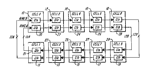
FIGURE 3 illustrates the configuration of a
ten cell domain, containing cells 0-9 interconnected
in accordance with the inventi.on in a dual ring bus
structure organize~ as ring A and ring B. Utilizing
plural rings is an important ieature of the
invention, which enables the system to continue
operating in the event of ~ingle point component
failures, and increases the bandwidth o~ the
interconnection system. In a preferred practice of
the invention, utilizing two rings, A and ~, rlng A
is configured ~or transfers involving even page
addresses in memor~, and ring B for odd page
address~s in memory. This interleaving mode is
-14- ~32~Q~3
1 discussed in greater detail hereinafter. Those
skilled in the art will understand that the invention
may be practiced in an embodiment having more than
two rings.
Rings A and B are preferably 50 megahertz
synchronous shift registers having plural data
storage stages with a 1~8 bit datapath width, as
indicated in FIGURE 3. Each of the cells 0-9
communicates with rings A and B through two
associated Cell Interconnects ~CIs~. As FIGURE 3
illustrates, cell interconnects 10-19 connect cells
0-9, respectively, to r;ng B, while cell
interconnects 20-29 connect cells 0-9, respectively,
to rinq A.
A preferred cell interconnect structure is
illustrated in FIGURE 4. Two cell interconnect units
(CIUs~ 72 and 73 and two 64K X 4 static RAMs (SRAMs)
70 and 71 are configured in pairs to form a single
cell interconnect 20. Similarly, cell interconnect
units 62 ~nd 63, and SR~Ms 60 and 61 are utilized to
form cell interconnect 10. Each cell interconnect
presents two 6~ bit data connections from its cell to
a respective ring (dmn_data) and one S4 bit
connection to its cell cache bus ~cache_data)~ The
structure and operation of such ~ cell cache bus are
described in Canadian Patent Application No. 582,560.
Through these connect;ons, the cell interconnect
moves req~ests and responses between th~ cell and a
respect;ve ring.
The ring connection~ of each cell
interconnect collectively form ~n input port and an
output port. In operation, each cell interconnect
~B .
-15- ~320~3
1 moves the data on its input port through two stages
(comprising ~our latches), modîfies the data as
required by a given cell interconnect unit operation
and presents the data on its output port.
Accordingly, when a number of cell interconnects are
linked in a loop, the delay stages form a shift
register such as Ring A or Ring B. Each cell
interconnect receiv~s data from the previous cell
interconnect in its ring and forwards data to the
ne~t. An insertion and extraction protocol described
in greater detail hereinafter allows the cell
interconnects to pass data between cells.
As FI~URE 4 illustrates, each cell
interconnect unit (CI) is formed by two cell
interconnect units (CIUsa, and associated SRAMs for
storing state bits. Each c~ll interconn2ct unit
~CIU), in turn, is constructed from a plurality of
integrated circuits. The integrated circuits which
form cell interconnect unit (CIU) 72 are depicted in
FIGURE 5.
The cache bus connection of the cel~
interconnect is a bî-directional interface. The cell
interconn~ct recsives data from the cache bus to send
to the ring and places data it receives from the ring
onto the cache bus to be serviced by the cache
control unit or domain routin~ unit. The structure
and operation of pref2rred cache control and domain
routing units are described in Canadian Patent No.
5~2,560.
~L 3 ~ 3
-16-
1 As illustrated in FIGURE 6, each cell
interconnect contributes two shift register stages to
the ~hift register structures of rings A and ~. For
example, a ring with ten cell interconnects, such as
rings A and B ~hown in FIGURE 6, consists of twenty
pipeline stages. Each pipeline ætage is capable of
selectively storing and transferring an
information-repxesentative signal representing one
data word. All data words circulate throu~h the ring
by progressing, in parallel, at the rate of one stage
per applied clock cycle. It is this feature o the
invention which allows each cell to uni~uely identify
the source and destination of each data word on the
bus, an~ determine appropriate processing steps for
each data word. One example of a preferred clock
signal distribution ~onfiguration is depicted in
FIGURE 7.
In accordance wlth the invention, cell
interconnect unit (CIU) 72 is constructed from
periphery unit 30, CIU tag unit 81, SRAM control unit
8~, cache ~us control unit 83, CIU data path unit 84,
CIU master control unit 85, and CIU directory unit
86. The integrated circuits illustrated in FIGURE S
~ontain latches, FIFO b~ffers, multiplexors (MUXs~
and other conventional logic ~lements.
In particular, the CIU datapath associated
wi~h CIU datapath circuit 84 is a 36 bit wide
datapath including low ana high cache group units, an
extract FIFO and an insert FIFO. These four units
collectively provide paths or (i) moving addre~ses
-17- ~37J~3
1 from the domain interconnected by rings A and B, and
from the cache bus, to the directory for address
lookup, ~ii) moving packets through the two pipeline
stages of each CIU, (iii) moving packets from the
domain to the cache bus, and (iv) moving packets from
the cache bus to the domain.
~he low and high cache group units direct
appropriate addresses to the CIU directory circuit 86
or lookup, and provide mo~ification of directory
entries. In particular, the cache group units can
pass domain~ cache or recirculated addresses for
lookup operations, modify directory entries, and move
data from directory 86 to the associated cache bus.
The extract FIFO unit mo-es data from the
CIU domain inputs into a holding register file, and
subsequently passes the data to the associated cache
bus. Th~ insert FIFO unit moves data from the cache
bus ;nputs into a holding reg;ster file, and
subsequently passes this data to the CIU domain
outputs. Addit;onally, the insert FIFO uni~ provides
for modifying packets on the domain formed by rings A
and B. The datapath control section associa~ed with
CIU datapath unit 84 receives commands from the
master control unit 85 and converts them into comman~
signals for use by the elements of the CIU datapath.
Detailed schematics and timing diagrams ~or the
elements o~ these integrated circuits are set forth
in ~lGVRES 9 to 18.
Top level control of the CIU 72 is managed
by the CIU master control circuit 85, the ~RAM
.
-18- ~3~ 3
1 control circuik 82, and the ca~he bus control CiL'CUit
83. The master control circuit 85 receives PACKET
HEADER and EMPTY STATUS bits, and provides sequencing
to the directory block to perform address lookups,
The master control circuit 85 utilizes the results of
these lookup operation~ to determine which of the
PASS, EXTRACT and INSERT operations, discussed in
greater detail hereinafter, is appropriate. The
master control circuit 85 performs these operations
based upon signals from the CIU data path circuit 84
and cache bus control circuit 83.
The SRAM control circuit 82 generates
control signals for addressing the external SRAMS 70
and 71 used by the CIU 72 and illustrated in FIGURE
4. The cache bus control circuit 83 manages
arbitration and flow control on the cache ~us, as
described in Canadian Patent Application No. 58~,560.
The cache bus control circuit ~3 receives command signals
from the master control circuit 85, and in turn,
tran~mi~s status report signal~ to the master control
circuit ~5.
Siqna1s and
As FIGURE 7 illustrates, a single domain
clock signal ~h,l), ~enerated by clock generator 30,
is distributed to the entire domain interconnect
formed by rings A and B. Domain clock (h,l) provides
50mh~ æynchronous timing information to the cell
interconnects within the domain interconnect ~ormed
by rings ~ and B.
By properly distributing domain clock (h,l~,
the effective clock ~kew for a cell interconnect such
'
~3~0~3
--19--
1 as, for e~ample, the cell interconnect 14
corresponding to cell 4, is the clock skew between
that cell interconnect's input stage 14.0 and prior
adjacent cell inter~onnect (cell 2) and its output
stage 14.1 and nest adjacent cell (cell 6). An
important advantage of the invention is that clock
~kew is not accumulative, and propagation time
between cell interconnects is independent of the
number of cell interconnects or stages.
The fundamental result is that the clock
cycle time --i.e. the inverse of the clock fr~quency
-- of the domain interconnect is simply the cycle
time between two adjacent cell interconnects. The
lS clock cycle time does not increase and requency does
not decrease as the number of cell interconnects is
increased. Thus, as the number of cell interconnects
in a ring is increased, the flux of operations
through the ring is constant, while the number of bus
operations which can be e~ecuted during a complete
bus cycle increases linearly. 'rhis is an important
feature of the invention, which is ideally suited for
multiprocessor structures.
The high ~peed nature o~ a domain
interconnect constructed in accordance with the
invent;on is further enhanced by two topological
factor~. First, the output (i.e. second~ stage of
each cell interconnect ~ives a single load, ~he
input ~tage of the adjacent cell interconnect.
Second, each cell interconnect requires connection to
only its two neighboring cell interconnect~, allowing
close pro~imity of all directly connected cell
interconnects. Thi~ combination of absolute minimal
~32~3
l loading and very short physical distance between
adjacent cells minimizes propagation time between
cell interconnect~.
Those skilled in the art will understand
that while the ambodiment described above in
connection with FIGURE 7 utilizes a synchronous
clock, the invention can be practiced in connection
with an asynchronous or self-timed clock
confi~uration.
In accordance with the invention, data
circulating through a given ring is divided into data
packets of ten data words, corresponding to ten shift
register ring stages. The nurnber of shift register
stages must be an exact multiple of the number of
data worcls in a data packet. Given, for example, a
ring with twenty cells and two register stages per
cell, the ring consists of forty staqes. Thus, four
ten-word packets can be transferred simultaneously in
this ring~ This property is generalized below in
Table I.
Number of CI Number of Stages Number of Packets
2~ 2
2~ 40 4
: : .
': . . - . ~ ,
.
.
~. :
-21- ~ 3 ~ 3
1 The invention is preferably practiced ~n
connection with the packet configuration shown in
FIGURE 8. The first data word in each half is an
address, the second data word is a command and the
remainin~ data words are data, as indicated in FIGURE
B. Those skille~ in the art will understand that
alternative packet configurations are possible and
within the ~cope o~ the invention.
In addition to the operations described
abov~, a cell interconnect can modify the com~and
field of a packet. For example, a cell interconnect
can extract a packet by copy;ng the packet from the
ring and changing the command field to EMPTY.
Alt~rnatively, if a cell interconnect merely copies a
packet, the command field would remain unchanged,
allowing the packet to continue to circulate through
the ring.
All packets circulate through the domain
interconnect only once. This property results from
an operational protocol in which each operation is
created and retir~d by the same cell interconnect.
Cells which extract a packet to add response data
must later re-insert the packet.
The operations that the cell interconnect
units can perform on packets thus include the
following:
PA~S PACKET: The cell interconnect unit
passes a packet from its ring inputs to its ring
outputs w~thout any modification if the packet
5
-~2- ~320~03
1 specifies an address of which the cell interconnect
has no knowledge.
EXTRACT PACKET: The cell interconnect unit
extracts a packet from the ring if it represents a
request the cell interconnect unit made to the ring
or contains an address the cell interconnect unit
must act upon. When a cell interconnect unit
extracts a packet from the ring it modiies the
command of the packet to indicate the extractionO
SEND PACKET to the Cache Bus: The cell
interconnect unit sends each packet that it extracts
from thë ring to the cache bus for service by the
cache controller.
RECEIVE PACKET from the C~che Bus: The
cache controller can send a packet to the cell
interconnect unit for insertion into the ring. The
cell interconnect unit receives these packets and
retains them until they can be inserted into the ring.
INSERT PACKET: Th~ cell interconnect unit
inserts a packet into the ring whenever it has a
packet awaiting insertion and t:he current ring packet
is marked as EMPTY.
In a preferred embodiment o~ the invention,
the domain interconnect formed by rin~s ~ and B
supports two sets o~ fields, referred to as the
domain ields and the cell interconnect uni~ f;~lds.
The dsmain fields are established by serial
connections from one cell interconnect to the next
,
~ . ~
-23- ~3~ 3
1 cell interconnect, which form a ring. Each cell
interconnect has a separate r~ceive and transrnit port
or the domain fields, as indicated in FIGURE 4. The
cell interconnect unit fields provide communication
among the cell interconnect units of the cell. The
domain fields are summarized below in Table ~I:
TABLE II: DOMAIN FIELDS
DOMAIN DATA
DOMAIN ECC
DOMAIN ~EADER
DOMAIN CLOCK
CIU ID
CIU CELL ADDRESS
CIU EXTRACT
The DOMAIN DATA and DOMAIN ECC fields are
responsible for movin~ the dat~ of ring operations.
Each operation is a packet of ten domain bus
transfers. The DOMAIN HEADER field marks the
beginning of an operationD The! DOMAIN CLOCK field
provides ~iming for the shift register structure in
cooperation with the clock generator ;llustrated in
Figure 7. The CIU ID field identifies the type of
cell interconnect unit involved in a given transfer.
The CIU CE~L ADDRESS field identifi~s the domain
local address of the cell. The CIU EXTRACT field
communicates information between cell interconnect
uni ~.
I~ operation, the DOMAIN DATA field
transmits the address, command, and data information
5
-24 L3200~3
corresponding to an operation~ The~ conf iguratiorl o~
the DOMAIN DATA field consists first of an address,
then a cornrnand, and inally eight data v~luesO one or
more of which may be empty.
The DOMAIN ECC field transmits a Hamming
base~ error correction code (ECC) word for eac~
domain data transfer. DOMAIN ECC is not generated or
checked by the cell interconnect unit~, but passed
unchanged to the target units.
The DOMAIN HEADER field designates a given
word in the current domain data transfer as the first
word of a packet.
The assertion of the DO~AIN RESET signal by
the domaln structure or domain power controller
causes each cell interconnect and corresponding cell
to enter a reset state. The reset state is described
in Canadian Patent Application No. 582, 560.
The assertion of CELI, RESET by a ell causes
the corresponding cell and ~ell interconnect to
reset. When reset, cell interconnects perform only
P~SS PACKET operations.
The c~ll interco~nect unit control fi~lds
provide for communic~ti~n specific to the cell
interconnect units. These cell interconnect unit
co~trol ~ields are summarized below in Table III.
~32~3
-25
TABLE IIT: CIU Control Field~
CIU ID
CIU EXTRACT
CIU CELL ADDRESS
THE CIU ID ield for each CIU is established
by the configuration of electrical connections rom
the CIU to power and ground terminals. Thi~
configuration establishes a unique CIU identification
number for each CIU. The interpretation of the
identification number depends upon whether the plural
ring structure is configured in a two-way or a
four-way memory interleaving mode. Normally, riny A
is configured for even page addresses in memory and
ring B for odd page addresses in memory. However,
those skilled in the art will appreciate that the
shift register structure can be! c~nfigured to pass
all addresses on either riny. ~Page address
; interleaving is normally configur~d at s~stem
configuration time by control locations in the cell
- interconnec~s. Table IV below summarizes
interpretation of id numbers in the two-way
interleaved mode.
T~E D: TW0 WA~ INTERLE~V~
ID VALUE DEFIN~TI0
o M~ster CIU 1
1 Master CIU 1
a Slave CIU 0
~ Slave CIU 1
'' ' ~
26 ~32~
1 Tabl2 V below summarizes int~rpretation of id numbers
in the four-way interleaved mode:
T_E ~T . FOUR WAY I NTERLEAVE12
ID VALUE DE:FINIT.ION
o M~STER 0
1 Master CIU 1
2 Master CIU 2
3 Master CIU 3
When two CIUs are partnered as master and
slave, the slave cell interconnect unit drives a
one-bit CIU EXTRACT signal which is read by its `!
partner master cell interconnect unit. The CIU
EXTRACT ~ignal is asserted or de-asserted accordinq
to whether the slave CIU identifies the current
operation as requiring removal from th~ shift
register structure.
Th~ CIU CEL~ ADDRESS sign~l represents khe
address within the domain of tlle cell asser~ing the
: signal.
In accordance with the invention, ~11 domain
interconnect tran~fers form a single packet. The
domain interconnect formad by the plural rings iæ
initialized to co~tain a figed number of~ packets
base~ on the number o~ cell interconnect For
-e~ampIe, 3 twenty cell doma;n interconnect contains
eight packets per ring. Thus, in this esample, eigh~
: : .
-27- ~20~03
1 packets per ring, or s;xteen packets per domai~
interconnect, can be transferred in parallel.
In a preferred practice of the invention in
conjunction with a multiprocessor structure like that
described in Canadian Patent Application No. 5B2,560, th~
c~ll interconnect performs two levels of interpretation in
order to determine how to operate on a packet~ First, the
cell interconnect examines the address specified in the
packet. The cell interconnect may be configured to
operate as a positive or a negative fil~er. As positive
filter, it operates on any System Virtual Address (SVA)
that has an entry in its cache descriptors. The
interaction of SVA addresses and cache descriptors is
further described in Canadian Patent Application NoO
582,560. The positive filter configuration is used when a
cell interconnect i~ connected to a cache either directly
or by a remote interface. The ne~ative filter
configuration is used when the cell interconnect is
connected to a rout~r. In ei~her configuration, the cell
interconnect operates on SVA addresses directed to it.
.
Secon~ly, having recognized an address, the
cell interconnect esamines the command portion of the
packet to determine if it ~an modify the response
field of the command and allow the packet to proceed,
or whether it must extract the packet from the domain
- in~erconnect.
A cell interconnect can insert a packet i~to
the ring when an empty packet arrives. An empty
packet is indicated by an IDLE operation type in the
.
-28_ :L32~3
cornrnand word of the packet. Evenly distributed usage
of the packets of the ring is provided by the
invention because no cell interconnect can use a
packet that it has just emptied by an extraction
operation. In order to perform an insertion, th2
cell interconnect must place its operation into the
ten consecutive stages of the empty packet.
It will be understood that given the plural
ring structure of the invention, the cell
intarconnect which initially injects a particular
operation into the ring will eventually receive that
operatiQn back. At that time, the cell interconnect
destroys the operation by changing the command word
to IDLE. Any cell interconnect that removes an
operation it did not create must return that
operation to the ring.
A cell interconnect e:~tracts an operation
from the ring by copying ;ts contents from the ten
consecutive stages of its packet and writing thP IDLE
operation type into the commant3 word of the packet.
Any cell interconnect that e~tracts an operation i~
did not create mus~ return tha1; operation to the rin~.
The bus structures are initialized in two
stepæ. First, th~ domain stages are formatted into
ten word packet~ by initiallzing the domain header
signal. Secondly, each packet is initialize~ ~o an
ID~ state. ~ the number of stages in either ring
is not an even multiple of ten stages, or if the
ci2cular path is logically broken, the ring will not
initialize.
-29- ~320~a3
In a preferred embodim~nt of the invention,
bus initialization is performed by software~ with
cell interconnect as~ist. Within each cell
interconnect is a DOMAlN HEADER STATUS bit which
indicates whether the domain is properly formatted by
verification of the DOMAIN HEADER ~ignal. If th~
DOMAIN HEADER STATUS bit indicateæ that a given ring
is improperly formatted, then a SETUP DOMAIN command
issued by a given cell to a cell interconnect
performs domain initializat;on.
It will thus be seen that the invention
efficiently attains the objects set forth above,
among those made apparent from the preceding
description. It will be understood that changes may
be made in the above construct;on and in the
foregoing sequences of operation without departing
from the scope o~ the invention. It is accordingly
intended tha~ all matter c~ntained in the above
description or shown in the accompanying drawings be
interpreted as illustrative rather than in a limiting
sense.
It is also understood that the ollowing
claims are intended to cover all of the generic and
specific features of the inve~tion as described
herein, and all statements of the scope of the
invention which, as a matter of language, might be
æaid to fall therebetween.