Note: Descriptions are shown in the official language in which they were submitted.
1 320072
LIGHT RECEIVING MEMBER
FIELD OF THE INVENTION
This invention relates to an improved light receiving
member sensitive to electromagnetic waves such as light
(which herein means in a broader sence those lights such
as ultra-violet rays, visible rays, infrared rays, X-rays
and y-rays~.
BACKGROUND OF THE INVENTION
For the photoconductive material to constitute an
image-forming member for use in solid image pickup device
or electrophotography, or to constitute a photoconductive
layer for use in image-reading photosensor, it is required
to be highly sensitive, to have a highsjN ratio (photo-
current (Ip)/dark current (Idl), to have absorption spectrum
characteristics suited for the electromagnetic wave to be
lrradiatec, to be quicklyresponsive and to have a desired
.~
resistance. It is also required to be not harmful to living
thlngs, especially man upon use.
:
. Other than~those requirements:, it is required to have
a property o~ moving a residual image within a predetermined
.
.
1 320072
period of time in solid image pickup device.
Particularly for the image-forming member for use in
an electrophotographic machine which is daily used as a
business machine at office, causing no pollution is indeed
important.
From these standpoints, the public attention has been
focused on light receiving members comprising amorphous
materials containing silicon atoms (hereinafter referred
to as "A-Si"j, for example, as disclosed in Offenlegungsschriftes
Nos. 2746967 and 285S718 which disclose use of the light
receiving member as an image-forming member in electrophotography
and in Offenlegungsschrift No. 2933411 which discloses use
of the light receiving member in an image-reading photosensor.
For the conventional Llght receiving members comprising
; ~A-Si materials, there have been made improvements in their
optical, electric and photoconductive characteristics such
as dark resistance, photosensitivity, and photoresponsiveness,
use-environmental characteristicsj economic stability and
durability.
However, there are still left subjects to make further
mprovements in their characteristics in the synthesis
situation in order to make such light receiving member
practically usable.
, ,
For example, in the case where such conventional light
receiving member is used as an image-forming member in
~:
'' '' ' ., ,'.
; :
1 320072
electrophotography with aiming at heightening the photo-
sensitivity and dark resistance, there is often observed
a residual voltage on the conventional light receiving
member upon use, and when i~ is repeatedly used for a
long period of time, fatigue due to the repeated use will
be accumulated to cause the so-called ghost phenomena
inviting residual images.
Further, in the preparation of the conventional light
receiving member using an a-Si material, hydrogen atoms,
halogen atoms such as fluorine atoms or chlorine atoms,
elements for controlling the electrical conduction type such
as boron atoms or phosphorus atoms, or other kinds of atoms
for improving the characteristics are selectively incorporated
in a light receiving layer of the light receiving member as
the layer constituents.
However, the resulting light receiving layer sometimes
becomes accompanied with defects on the electrical character-
istics, photoconductive characteristics and/or breakdown
voltage according to the way of the incorporation of said
constituents to be employed.
That is, in the~case of using the light receiving member
haYing such light r~eceiving layer, the life of a photocarrier
generated in the Iayer with the irradiation of light is not
sufficient, the inhibition of a charge injection from the
side of the substrate in a dark layer region is not sufficiently
1 320072
carried out, and image defects likely due to a local break-
down phenomenon ~the so-called "white oval marks on
half-tone copiesl')or other image defect~s likely due to
abrasion upon using a blade for the cleaning (the
so-called "white line")are apt to appea;r on the transferred
images on a paper sheet.
Further, in the case where the above light receiving
member is used in a hu~.id atmosphere, or in the case -
where after being placed in that atmosphere it is usedr
the so-called "image flow" sometimes appears on the transferred
images on a paper sheet.
Further in addition, in the case of forming a light
receiving layer of a ten and some m~ in thickness on an
appropriate substrate to obtain a light receiving member,
the resulting llght receiving layer is likely to invite
undesired phenomena such as a thinner ~pace being
formed between the bottom face and the surface of the
substrate, the layer being removed from the substrate and
a crack being generated within the layer following the lapse
of time after the light receiving member is taken out from
the vacuum deposition chamber.
These phenomena are apt to occur in the case of using
a cylindrlcal substrate to be usually used in the field of
electrophotograph~.
Moreover, there have been proposed various so-called
~
' 1' ,S' ~
. .
,
1 320072
laser printers using a semiconductor laser emitting ray as
the light source in accordance with the electrophotographic
process. ~or such laser printer, there is an increased
demand to provide an improved light receiving member of
having a satisfactorily rapid responsiveness to light in
the long wave region in order to enhance its function.
In consequence, it is necessitated not only to make a
further improvement in an A-Si material itself for use in
forming the light receiving layer of the light receiving
member but also to establish such a light receiving member
which will not invite any of the foregoing problems and to
satisfy the foregoing demand.
~;:
SUMMARY OF THE INVENTION
` The object of this invention is to provide a light
::
`~ receiving member comprlsing a light receiving layer mainly
composed of A-Si, free from the foreging problems and
~; capable of satisfying various kind of requirements.
` That is, the main object of this invention is to
provide a light recelving member comprising a light
, ,
recelving layer constituted with A-Si in which electrical,
optical and photoconductive properties are always substan-
~ :: ~ : : : :
tially stable and~hardly depend on the working circum-
stances, and whichare excellent against optical fatigue,
!
, S
'
',
1 320072
causes no degradation upon ~epeated use, excellent in
durability and moisture-resistance, exhi.bits little or no
residual potential and provides easy production control.
Another object of this invention is to provide a
light receiving member comprising a light receiving layer
composed of A Si which has a high photosensitivity in the
entire visible region of light, particularly, an excelent
matching property with a semiconductor laser with
rapid light response.
Another object of this invention is to provide a light
receiving member comprising a light receiving layer composed
of A-Si which has high photosensitivity, high S/N ratio and .
high electrical voltage withstanding property.
A further object of this invention is to provide a
light receiving member comprising a light receiving layer
composed~of A-Si which is excellent in the close bondability
:::
; between a substrate and a layer disposed on the substrate or
between each of the laminated layers, with a dense and
stable structure.and~of high layer quality.
: .:
.;
:~ ~
:
. ..
. '
.' " .,'. , ' ' '~
': ,, ' : .
1 320072
These and other objects, as well as the features of this
invention will become apparent by reading the following
descriptions of preferred embodiments according to this
invention while referring to the accompanying drawings.
BRIEF DESCRIPTION OF THE DRAWIN~S
Figure 1(A) and 1(B) are views of schematically
illustrating representative examples of the light
receiving member according to this invention.
Figures 2 through 10 are views illustrating the
thicknesswise distribution of the group III atoms or the
group V atoms in the first layer of the light receiving
member according to this invention, the ordinate represent-
ing the thickness of the layer and the abscissa
representing the distribution concentration of respective
atoms.
Figure 11 is a schematic explanatory view of a fabrica-
tion device by glow dlscharing process as an example of
the device for preparing the first layer and the second
layer respectively of the light receiving member according
to this inventionO
Figures 12 through 15 are views illustrating the
variations in the gas flow ratios in forming the first
,
1 320072
layers according to this invention, wherein the ordinate
represents the thickness of the layer and the abscissa
represents the flow ratio of a gas to be used.
DET~ILED DESCRIPTION OF THE INVENTION
The present inventors have made earn~st-studies for
overcoming the foregoing problems on the conventional
light receiving members and attaining the objects as
described above and, as a result, has accomplished this
invention based on the finding as described below.
As a result of the earnest studies focusing on
materiality and practical applicability of a light
receiving member:comprlsing a:light receiving layer
composed A-Si for use in electrophotography, solid image-
pickup device and image-reading device, the present
inventors have obtained the following findings.
~ This is, the present inventors have found that in
:~ case where the light receiving layer compose of an
; :~amorphous material~containing sil1con atoms~as the main
constituent atoms is so structured as to have a particular
i:
~: ~two-layer structure as later described, the resulting
: : light receiving member pr~y1~es many practically applicable
excel;lent characteristics especially usable for electro-
photography which~are superior to the
, ~,, . ~ . . . ..
'' ', . ~ :
~' ~
,
1 320072
conventional light receiving member in any of the
requirements.
In more detail, the present inventors have found that
when the light receiving layer is so structured as to have
two layer structure using the so-called hydrogenated
amorphous silicon material~ halogenated amorphous silicon
material or halogen-containing hydrogenated amorphous
silicon material, namely, represented by amorphous materials
containing silicon atoms as the main constituent atoms (Si),
and at least one of hydrogen atoms (H) and halogen atoms ~X)
[hereinafter referred to as "A-Si ~, X)], the resulting
light receiving member becomes such that brings about the
foregoing unexpected effects.
Accordingly, the light receiving member to be provided
according to this invention is characterized as comprising
a substrate and a light receiving layer having a first layer
of having photoconductivity which is constituted with an
amorphous material containing silicon atoms as the main
const1tuent atoms and an element for controlling the
conductivity heing:unevenly:distributed in .-
the entire:layer region or in the partial layer region
adjacent to the substrate and a second layer which is
constltuted with an amorphous material containing silicon
:atomC as the main constituent atoms, carbon atoms and an
element for controlling ~he conductivity in the state o~
~ ` '
'~.'G~
.
.
1 320072
being uniformly distributed.
The first layer may also contain germanium atoms in an
uniformly distributed state in the entire layer region or
in the partical layer region adjacent to the substrate.
As the amorphous material containing silicon atoms
as the main constituent atoms to be usecl for the formation
of the first layer, there can be the so-called
hydrogenated amorphous silicon, halogenated amorphous silicon
and halogen-containing hydrogenated amorphous silicon,
namely, represented by amorphous materials containing silicon
atoms (Si) as the main constituent atoms and at the least
one kind selected from hydrogen atoms (H) and halogen atoms
(X) [hereinafter referred to as "A-Si(H,X)"].
As the amorphous material containing silicon atoms
as the main constituent atoms to be used for the formation
~.
of the second layer, there is used an amorphous material
containing silicon atoms (Si) as the main constituent
atoms, carbon atoms ~Cj, and at least one kind selected
. :
from hydrogen atoms(H~ and halogen atoms(X)[hereinafter
referred to as "A-SiC(H,X)"~.
As the foregoing element for controlling the con-
: ductlvity,; there can be the so-called impurities
in the field of the semiconductor f and
;~ those usable herein can.include atoms belonging to the
:
~ Group III of the periodical table that provide p-type
~ " ,~
,
1 320072
conductivity (hereinafter simply referred to as "group
III atom") or atoms belonging to the group V of the
periodical table that provide n-type conductivity
(hereinafter simply referred to as "group V atom").
Specifically, the group III atoms can include B (boron),
Al (aluminum), Ga (gallium), In (indium) and Tl (thallium),
B and Ga being particularly preferred. The group V atoms
can include, for example, P (phosphorus),As(arsenic), Sb
(antimony) and si (bismuth), P and As being particularly
preferred.
In the case where both the first layer and the second layer
contain an element for controlling the conductivity, the kind of
the element to be contained in the first layer can be the
same as or different from that to be contained in the second
layer.
As the halogen atorn (X) to be contained in the first
layer and/or in the second layer in case where necessary,
there can he mentioned fluorine, chlorine, bromine and
icdine. Among~these halogen atoms, fluorine and chlorine -~
are most preferred.
The first layer and/or the second layer may contain
:: : ::
hydrogen atoms ! H ) where necessary.
~ ~ In that case, the amount of the hydrogen atoms (H),
; ~ the amount of the halogen atoms (X) or the sum of the amounts
for the hydrogen atoms and the halogen atoms(H~X) to be
~:,
,~ 11
1 320072
incorporated in the first layer and/or the second layer is
preferably 1 x 10 2 to 4 x 10 atomic %, more preferably,
5 x 10 2 to 3 x 10 atomic %r and, most preferably, 1 x 10 1
to 25 atomic %.
The light receiving member according to this invention
will now be explained more specifically referring to the
drawings. The description is not intended to limit the
scope of the invention.
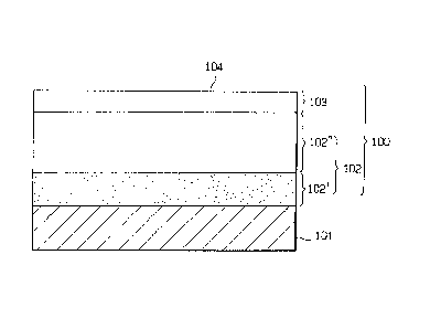
Figures 1(A) and 1(B) are schematic views illustrat-
ing the typical layer structures of the light receiving
member of this invention, in which are shown the light
receiving member 100, the substrate 101, the first layer
102 and the second layer 103 having a free surface 104.
Substrate (101)
The substrate 101 for use in this invention may either
be electroconductive or insulative. The electroconductive
support can include, for example, metals such as NiCr,
stainless steels, Al, Cr, Mo, Au, Nb, Ta, V, Ti, Pt and
Pb or the alloys thereof.
The electrically insulative substrate can include, for
example, films or sheets of synthetic resins such as
polyester, polyethylene, polycarbonate, cellulose acetate,
polypropylene, polyvinyl chloride, polyvinylidene chloride,
polystyrene, and polyamide, glass, ceramic and paper.
It is preferred that the electrically insulative substrate
12
" , ~ ,,
~ 320072
is applied with electroconductive treatment to at least
one of the surfaces thereof and disposed with a light receiv-
ing layer on the thus treated surface.
In the case of glass, for instance, electroconduc-
tivity is applied by disposing, at the surface thereof,
a thin film made of NiCr, A1, Cr, Mo, Au, Ir, Nb, Ta, V,
i, Pt, Pd, In203, SnO2, ITO ~In203 + SnO2), etc. In the
case of the synthetic resin film such as a polyester film,
the electroconductivity is provided to the surface by dis-
posing a thin film of metal such as NiCr, A1, Ag, Pv, Zn,
Ni, Au, Cr, Mo, Ir, Nb, Ta, V, Tl and Pt by means of vacuum
deposition, electron beam vapor deposition, sputtering,
etc., or applying lamination with the metal to the surface.
The substrate may be of any con~iguration such as
: : ,
cylindrical, belt-like or plate-like shape, which can be
properly determined depending on the application uses.
For instance, in the case of using the light receiving
member shown ln Figure l(A) and 1(B) as image forming member
for use ln electronic photography, it is desirably configurated
into an endless belt or cylindrical form for continuous high
.
; speed reproduction. The thickness of the
substrate member is properly determined so that the light
:
receivlng member as desired can be formed.
In the case where flexibility is required for the light
receiving member, it~can be made as thin as possible
, :~
,~ :
~ ~ 13
~, ~
.
1 320072
within a range capable of sufficiently providing the func-
tion as the substrate. However, the thickness is usually
greater than 10 ~m in view of the fabrication and handling
or mechanical strength of the substrate.
First Layer (102)
The first layer 102 is disposed between the substrate
101 and the second layer 103 as shown in Figures 1(A) and
1(B).
Basically, the first lyer 102 is composed of A-Si
(H,X) which contains the element for controlling the
conductivity, the group III atoms or the group Y atoms,
in the state of being distributed unevenly in the entire
layer region or in the partial layer region adjacent to
the substrate 10~1.
(Herein or herinafter, the uneven distribution means
that the distribution of the related atoms in the layer
is uniform ln the direction parallel to the surface of
the substrate but is uneven in the thickness direction.)
Now, the purpose and the expected effect of in-
corporating the element for controlling the conductivity
in the first layer of the light receiving member according
to this invention will vaEy depending upon its distribution
in the`layer aa below described~
~ That is, in the case of incorporating the element
., ~
14
s~ ., ,~ ,,
" . . . " . .
~ .
1 320072
largely in the partial layer region adjacent to the
substrate, the effect as the charge injection inhibition
layer is brought about. In this case, the amount of the
element to be contained is relativeiy large. In view of
this, it is preferably from 30 to 5 x 10⁴ atomic ppm, more
preferably from 50 to 1 x 10⁴ atomic ppm, and, most pre-
ferably, from 1 x 10² to 5 x 10³ atomic ppm.
Adversely in the case of incorporating the element
largely in the partical layer region of the first layer
adjacent to the second layer, if the conduction type of
the element is the same both in the first layer and the
second layer, the effect to improve the matching of energy
level between the first layer and the second layer and
to promote movement of an electric charge between the t~o
layers is brought about. And this effect is particularly
significant in the case where the thickness of the second
layer is large and the dark resistance of the layer is high.
Further, in the case of incorporating the element
largely~in the partial layer region of the first layer
adjacent to the second layer, if the conduction type of
the element to be contained in the first layer is dif-
ferent from that of the element to be contained in the
~:
second layer, the partial layer region containing the
element at high concentration functions purposely as the
- 15
.
.'
~ ' :
1 320072
-
compositon part and the effect to increase an apparent
dark resistance in the electrification process is brought
about.
In the case where a relatively large amount the element
is incorporated in the partial layer region of the first
layer adjacent to the second layer, in each case, the amount
of the element is sufficient to be relatively small.
In view of this, it is preferably from 1 x 10 3 atomic
ppm, more preferably from 5 x 10 2 to 5 x 10² atomic ppm,
and,most preferably, from 1 x 10 1 to 5 x 10² atomic ppm.
In the following, an explanation is made on the typical
example when the thicknesswise distributing conc~ntration
of the element for controlling the conductivity is uneven,
with reference to Figures 2 throuqh 10.
In the typical embodiments shown in Figuxes 2 through 10,
in whlch the;group III or group V atoms incorporated into the
light first layer are so distributed that.the amount therefor
is relatively great on the side of the substrate, decreased
from the substrate~toward the free surface of the light
receiving layer,:and is relatively smaller or substan-
tially equal~to zero~near the end on the side of the free
surface
In Figures 2 through lo, the abscissa represents
:the distribution concentration C of the group III atoms
~;,
or group~ V atoms;and:the ordinate represents the thickness
: :
16
, ~
~! , ~
' . '
~ ' ,
1 320072
of the first layer; and tB represents the intexface
position between the substrate and the first layer and
tT represents the interface position between the ~irst
layer and the second layer.
Figure 2 shows the first typical example of the thick-
nesswise distribution of the group III atoms or group V
atoms in the light receiving layerr In this example, the
group III atoms or group V atoms are distributed such that
the concentration C remains constant at a value C1 in the
range from position t1 to position tT~ where the concentra-
tion of the group III atoms or group V atoms is C3.
In the example shown in Figure 3, the distribution
concentration C of the group III atoms or group V atoms
contained in the first layer is such that concentration
C4 at position tB continuously decreases to concentration
C5 at position tT.
In the example shown in Figure 4, the distribution
concentration C of the group III atoms or group V atoms
lS such that concentration C~ remains constant in the range
from position t~to position t2 and~it gradually and con-
t;inously decreases in the range from position t2 to
position tT. The concentration at position tT is
substantially zero. ("Substantially zero" means that the
concentration is lower than the detectable limit.)
In the example shown in Figure 5, the distribution
17
.
'
1 320072
concentration C of the group III atoms or group V atoms
is such that concentr~tion C8 gradually and continuously
decreases in the range from position tB to position tT~
at which it is substantially zero.
In the example shown in Figure 6, the distribution
concentration C of the group III atoms or group V atoms
is such that concentration Cg remains constant in the range
fxom position B to positi.on t3, and concentration C8
linearly decreases to concentration C10 in the range from
position t3 to position t~,.
In the example shown in Figure 7, the distribution
concentration C of the group III atoms or group V atoms
is such that concentration Cll layer region near the second
layer, the foregoing effect that the layer region A where
the group III or group V atoms are distributed at a higher
concentration can form the charge injection inhibition
layer as described above more effectively, by disposing
,
a locali.zed region A where the distribution concentration
of the group III~or~group V atoms is relatively higher
at the portion near~the slde of the support, preferably,
:
by~disposing the localized region A at a position within
5 ~m from the~interface position~adjacent to the substrate
surface. : ` ~
As above-mentloned, the distribution state of the
group~III or group V atoms in the first layer of this
: :
:
~ 18
~ . . .. . . .
- 1 320072
invention is determined properly based on a desired purpose.
This situation is apparent from what are mentioned in Figures
2 through 10, which are, however, the typical examples.
That is, in other distribution states than those mentioned
ahove may be taken. For example, in the case where the
concentration of the group III or group V atoms in the
partial layer region near the interface between the first
layer and the second layer is relatively high or in the
case where the concentration of the group III or group
V atoms in the center partial layer region is relatively
high, the modified distribution states based on.
Figures 2 through 10 can be properly and applicably
employed.
In order to lncorporate germanium atoms in the first
layer 102 of the light receiving member of this invention,
the germanium atoms are incorporated in the entire layer
region or in the partial layer region adjacent to the
substrate respectively uniformly distributed state.
In the case of inco~rporating germanium atoms in the
first layer, an absorption spectrum property in the long
wavelength region of the light receiving membker may be
. ~ ~
improved. That ia, the light receiving member according
to~this lnvention becomes~to give~excellent various pro-
perties by incorporating germanium at:oms in the first layer.
Particularly, it becomes more sensititve to light of
~::: :
~ .
,. .
';: ~;
1 9
'
: ' , .~ ' `;; .
,
. ' , - '
1 320072
wavelengths broadly ranging from short wavelength to long
wavelength covering visible light and it also becomes quickly
responsive to light.
This effect becomes more significant when a semicon-
ductor laser is used as the light source.
In the case of incorporating germanium atoms in an
uniformly distributed state in the entire layer region
of the first layer, the amount of germanium atoms to be
contained should be properly determined so that the object
of the invention is effectively achieved. In view of the
above, it is preferably from/to t x ]05 atomic ppm, and,
most preferably, from 1 x 10² to 2 x 10⁵ atomic ppm.
In the case of incorporating germanium atoms in the
partial layer region adjacent to the substrate, the
occurrence of the interference due to the light reflec-
t1on from the surface of the substrate can be effectively
prevented wherein a semiconductor laser is used as the
light source.
Figure l(B) is a schematic view illustrating the
typical layer constitution of the light receiving member
;in the case of~incorporating germanium atoms in the partial
layer region in the first layer in an uniformly distributed
state, in whlch are shown the substrate 101, the first
layer 102, a first layer region 102l constituted with
A-Si(H,X) containing germnium atoms in an uniformly
~ '
.,,
1 320072
-
distributed state [hereinafter referred to as "A-SiGe(H,X~",
a second layer region 102" constituted with A-Si(H,X)
containing no germanium atoms, and the second layer 103.
That is t the light receiving member shown in Figure
l(B) becomes to have a layer constitution that a first
layer region formed of A-SiGe(H,X) and a second layer region
formed of A-Si(H,X) are laminated on the substrate in this
order from the side of the substrate, and further the second
layer 103 is laminated on the first layer 102. When the
layer constitution of the first layer takes such a layer
constitution as shown in Figure ItB), particularly in the
case of using light of long wavelength such as a semicon-
ductor laser as the light source, the light of long
wavelength, which can be hardly absorbed in the second
; layer region 102", can be particularLy and completely
absorbed in the first layer region 102'. And this is
directed to prevent the interference caused by the light
reflected from the surface of the substrate.
The amount of germanium atoms contained in the first
layer region 102' should be properly determined so that
the object of the invention is effectively achieved.
It is preferably from 1 to 1 x 10⁷ atomic ppm, more
preferably from l x 102 - 9.5 x 10⁵ atomic ppm, and,
most preferably, from 5 x 10² _ 8 x 10⁵ atomic ppm.
The thickness (TB) of the first layer region 102'
and the thickness (T) of the second layer region 102"
~'
;i 21
i :~
. , .,, .
~, ;. ~. ~ ;
1 320072
are important factors for effectively at-taining the fore-
going objects of this invention, and they are desirably
determined so that the resulting light receiving member
becomes accompanied withmany desired practically applicable
characteristics.
The thickness (TB) of the first layer region 102'
is preferably from 3 x 10 3 to S0 ~m, more preferably
from 4 x 10 3 to 40 ~m, and, most preferably, from 5 x
10 3 to 30 ~m. And the thickness (T) of the second layer
region is preferably from 0.5 to 90 ~m, more preferably
from 1 to 80 ~m, and most preferably, from 2 to S ~m.
And, the sum (TB ~ T) of the thickness (TB) Eor the
former layer region and that (T) for the latter layer region
is desirably determined based on relative and organic
relationships with the characteristics required for the
first layer 102~
::
It is preferably from 1 to 100 ~m, more preferabIy
from l to 80 ~m, and, most prerferably, from 2 to 50 ~m.
Further, for the relationship of the layer thickness TB
and the layer thickness T, it is preferred to satisfy the
equation: TB/T <l,~more prefer~ed to satisfy the equation:
TB/T <0.9, and, mo~st;preferred to satisfy the equation:
TB/T <~0.8. In addition, for the layer thickness (TB)
of the layer reglon containing germanlum atoms, it is
necessary to be determined based on the amount of the
22
, .
., ,., ~
1 320072
germanium atoms to be contained in that layer region.
For example, in the case where the amount of the germanium
atoms to be contained therein is more than 1 x 10⁵ atomic
ppm, the layer thickness TB isdesignedto be remarkably
large.
Specifically, it is preferably less than 30 ~m, more
preferably less than 25 ~m, and, most preferably, less
than 20 ~m.
Second_Layer (103 ?
The second layer 103 having the free surface 104 is
disposed on the first layer 103 to attain the objects
chiefly of moisture resistance, deterioration resistance
upon repeating use, electrical voltage withstanding pro-
perty, use environmental characteristics and durability
for the light receiving member according to this invention.
The second layer is formed of an amorphous material
containing silicon atoms as the constituent atoms which
are also contained in the layer constitutent amorphous
material for the first layer, so that the chemical stability
at the interface between the two layers is sufficiently
secured.
Typically, the surface layer is formed of an amorphous
material containing silicon atoms, carbon atoms and
hydrogen atoms and/or halogen atoms in case where
~'
; ~ 23
"'''
'' ' .
:
.,
.
' :. ;, ' ~ ;
'' ~' ,-.
.
1 320072
necessary [hereinafter referred to as "A-SiC(H,X)"].
The foreging objects for the second layer can be effectively
attained by introducing carbon atoms structurally into
the second layer. And, the case of introducing carbon
atoms structurally into the second layer, following the
increase in the amount of carbon atoms to be introduced,
the above-mentioned characteristics will be promotedl but
its layer quality and -its electric and mechanical
characteristics will be decreased if the amount is
excessive.
In view of the above, the amount of carbon atoms to
be contained in the second layer is preferably 1 x 10⁻³
to 90 atomic %, more preferably 1 to 90 atomic %, and,
most preferably, 10 to 8~0 atomic %.
For the layer thi~kness~of the second layer, it is
desirable to be thickened. But the problem due to
generation of a residual voltage will occur in the case
where it is excesslvely thick. In view of this, by in-
corporating an element for controlling the conductivity
such as the group III atom or~the group V atom in the
s~econd layer, the~o~ccu;rrence of~the~above problem can be
effectively prevented~beforehand.~ In that case, ln
addition to the above effect, the second layer becomes such
that is free from any problem due to, for example, so-
called scratches ~hich will be caused by a cleaning
24
..,. . ' , . .
'
.
1 320Q72
means such as blade and which invite deEects on the trans-
ferred images in the case of using the light receiving
member in electrophotography.
In view of the above, the incorporation of the group
III or group V atoms in the second layer is quite benefi-
cial for forming the second layer having appropriate properties
as required.
And, the amount of the group III or group V atoms
to be contained in the second layer is preferably 1.0 to
1 x 10⁴ atomic ppm, more preferably 10 to 5 x 10³ atomic
ppm, and, most preferably, 102 to 5 x 10³ atomic ppm.
The formation of the second layer should be carefully
carried out so that the resultiny second layer becomes
such that brings about the characteristics required there-
for.
:: :
By the way, the texture state of a layer constituting
material which contains silicon atoms, carbon atoms, hydrogen
atoms and/or halogen atoms, and the group III atoms on
the group V atoms takes from crystal state to amorphous
state whlch show from a~semiconduct1ve property to an
insulative property for the electric and physical pro-
:
perty and which show from a photoconductive property to
a non-photoconduct1ve property for the optical and ele-
:
ctric property upon the layer forming conditions and the
amount of such atoms to be incorporated in the layer to
be formed.
, : , .
^ 25
:~ , . ' "
.. , . '.' ': ~ ' ' '
,
. .
- '
1 320072
In view of the above, for the formation of a desirable
layer to be the second layer 103 which has the required
characteristics, it is required to chose appropriate layer
forming conditions and an appropriate amount for each kind
of atoms to be incorporated so that such second layer may
be effectively formed~ For instance, in the case of dis-
posing the second layer 103 aiming chiefly at the
impro~ement in the electrical voltage withstanding property,
that layer is formed of such an amorphous material that
invites a significant electrically-insulative performance
on the resulting layer.
Further, in the case of disposing the second layer
103 aiming chiefly at the improvement in the deteriora-
tion resistance upon repeating use, the using charac-
teristics and the use environmental characteristics,
that lay is formed of such an amorphous material that
eases the foregoing electrically-insulative property to
some extent but bring about certain photosensitivity on
the resulting layer.
Further in addition, the adhesion of the second layer
~ 103 with the first layer 102 may be furthex improved by
-;~ incorporating oxygen atoms and/or nitrogen atoms in the
secoDd layer in a uniformly distributed state.
For the light receiving member of this invention,
the layer thickness of the second layer is also an
'
26
i
: '
'
-
1 320072
important factor for effectively attaining the objects
of this invention. Therefore, it is appropriately determined
depending upon the desired purpose.
It is, however, also necessary that the layer thick-
ness be determined in view of relative and organic relation-
ships in accordance with the amounts of silicon atoms,
carbon atoms, hydrogen atoms, halogen atoms, the group
III atoms, and the group V atoms to be contained in the
second layer and the characteristics required in relation-
ship with the thickness of the first layer.
Further, it should be determined also in economical
viewpoints such as productivity or mass productivity.
In view of the above, the layer thickness of the second
layer is preferably 3 x 10 3 to 30 ~mt more preferably
4 x 10 3 to 20 ~m, and most preferabLy, 5 x 10 3 to 10 ~m.
As above explained, since the light receiving member
of thls invention is structured~by laminatlng a special
first layer and a special second layer on a substrate,
almost all the problems`which are often found on the
conventional light~receivlng member can be effectively
overcome.
Further, the light receiving member of this inven-
tion exhibits not only significantly improved electric,
optical and photoconductlve characteristics~, but also
slgnificantly improved electrical voltage withstanding
27
1 320072
property and use environmental characteristics. Further
in addition, the light receiving member of this invention
has a high photosensitivity in the antire visible region
of light, particularly, an excellent matching property
with a semiconductor laser and shows rapid light response.
And when the light receiving member is applied for
use in electrophotography, it gives no undersired effects
at aIl of the residual voltage to the image formation but
gives stable electrical properties high sensitivity and
high S/N ratio, excellent light fastness and proper-ty for
repeating use, high image density and clear half tone.
At it can provide high ~uality image with high resolution
, ~
power repeatingly.
Preparation_of_First Layer (1021~and Second Layer ~103)
The method of forming the light receiving layer of
; the light receiving member will be now explained.
Each of the;first layer 102 and the second layer 103
to constltute the~light~receiving layer of the llght re-
ceiving member of this invention is properly prepared by
vacuum deposltlon method utillzing the discharge
phenomena such as glow discharging, sputtering and ion
p~lating methods wherein relevant gaseous starting
mater1als are selectively used.
, , .~
28
.
. ~ .
1 320072
These production methods are properly used selectively
depending on the factors such as the manufacturing condi-
tions, the installation cost required, production scale
and properties required for the light receiving members
to be prepared. The glow discharging method or sputtering
method is suitable since the control for thQ condition
upon preparing the layers having desired properties are
relatively easy, and hydrogen atoms, halogen atoms and other
atoms can be introduced easily together with silicon atoms.
The glow discharging method and the sputtering method
may be used together in one identical system.
: ,
Preparation of First Layer (102~
Basically, when layer constituted with A-Si(H,X) is
formed, for examplej by the glow discharging method, gaseous
starting material capable of supplying silicon atoms (Si)
are introduced together with gaseous starting material
for introducing hydrogen atoms tHi and/or halogen atoms
~X) into a depositian chamber the inside pressure oE which
can be~reduced, glow discharge is generated in the deposition
chamber, and a layer composed of A-Si(H,X) is formed on
the surface of a substrate placed in the deposition
chamber.
The gaseous starting material for supplying Si can
include gaseous or gasifiable silicon hydrides (silanes)
4~ 2H6' Si3H8, Si4EIlo, etc., SiH4 and Si H
:
:' .~ ~
29
1 320072
being particularly preferred in view of the easy layer
forming work and the good efficiency for the supply of
si .
Further, various halogen compounds can be mentioned
as the gaseous starting material for introducing the halogen
atoms, and gaseous or ~asifiable halogen compounds, for
example~ gaseous halogen, halides, inter-halogen compounds
and halogen-substituted silane derivatives are preferred.
Specifically, they can include halogen gas such as of
fluorine, chlorine, bromine, and iodine; inter-halogen
compounds such as BrF, ClF, ClF3, BrF2, BrF7, IF , ICl,
IBr, etc.; and silicon halides such as SiF4, Si2F6, SiC4,
and SiBr4. The use of the gaseous or gasifiable silicon
halide as described above is particularly advantageous
since the layer constituted with halogen atom-containing
A-Si:H can be formed with additional use of the gaseous
starting silicon hydxide material for supplying Si.
In the case of forming a layer constituted with an
amorphous materlal containing halogen atoms ! typically,
a mixture of a gaseous silicon halide substance as the
starting material for supplying Si and a gas such as Ar,
H2 and He is introduced into the deposition chamber having
,
: a substrate in a predetermined mixing ratio and at pre-
: ~
determined gas flow rate, and the thus introduced gases
are exposed to the action of glow discharge to thereby
:~,
"~
~ 30
1 320072
cause a gas plasma resulting in forming said layer on the
substrate.
And, for incorporating hydrogen atoms in said layer,
an appropriate gaseous starting material for supplying
hydrogen atoms can be additionally usecl.
Now, the gaseous starting material usable for supply-
ing hydrogen atoms can include those gaseous or gasifiable
materials, for example, hydrogen gas (H2), halides such
as HF, HCl, HBr, and HI, silicon hydrides such as SiH4,
Si2H6, Si3H8, and Si4H10, or halogen-substituted silicon
hydrides such as SiH2F2, SiH2I2, SiH2C12, SiHC13, SiH2Br2,
and SiHBr3. The use of these gaseous starting material is
advantageous since the content of~the hydrogen~atoms ~H),
which are extremely effective in view of the control for
the electrical or photoelectronic properties, can be con-
:
trolled with ease. Then, the use of the hydrogen halideor the halogen-substituted silicon hydride as described
above is partlcularly advantageous since the hydrogen
atoms (H~ are also introduced together with the introduc-
tion of the halogen~atoms. ~ ~
The amount~of~the~hydrogen atoms (H) and/or the amount
of the halogen atoms (X) to be contained in a layer are
ad~usted propelly by~controlllng related conditions, for
example, the temperature of;a substrate, the amount of
a gaseous starting material capable of supplying the
`~' ,
.:
31
'
1 320072
hydrogen atoms or the halogen atoms into the deposition
chamber and the electric discharging power.
In the case of forming a layer composed of A-Si(H,X)
by the reactive sputtering process, the layer is formed
on the substrate by using a Si target and sputtering the
Si target in a plasma atmosphere.
To form said layer by the ion-plating process, the
vapor of silicon is allowed to pass through a desired gas
plasma atmosphere. The silicon vapor is produced by heating
polycrystal silicon or single crystal silicon held in a
boat. The heating is accomplished by resistance heating
or electron beam method [E.B. method~.
In either case where the sputtering process or the
on-plating process is employed, the layer may be lncor-
porated with hal~ogen atoms by introduclng one of the
above-mentioned gaseous halides or halogen-containing
silicon compounds into the deposition chamber in which
a plasma atmosphere of the gas is produced. In the case
.~
where the layer is incorporated with hydrogen atoms in
accordance with the sputtering process, a feed gas to liberate
: ~ :
~ hydrogen is introduced into the~deposition chamber in
: ~ :
~which~a plasma atmosph~ere of the gas is produced. The
feed gas to l;lberate hydrogen atoms includes H2 gas and
the above-mentioned silanes.
~ ! ~
~ For the format;ion of the layer in accordance with
:~ :
"
- 32
,~ .
1 320072
the glow discharging process, reactive sputtering
process or ion plating process, the foreging halide or
halogen-containing silicon compound can be effectively
used as the starting material for supplying halogen atoms.
Other effective examples of said material can include hydrogen
halides such as HF, HCl, HBr and HI and halogen-substituted
silanes such as SiH2F2, SiH2I2, SiH2C12, 3 2 2
and SiHBr3, which contain hydrogen atom as the constituent
element and which are in the gaseous state or gasifiable
substances. The use of the gaseous or gasifiable hydrogen-
containing halides is particularly advantageous since,
at the time of forming a light receiving layer, the
hydrogen atoms, which axe extremely effective in view of
controlling the electrical or electrophotographic pro-
.~
perties, can be introduced into that layer together withhalogen atoms. ~
The structural lntroduction of hydrogen atoms into
the layer can be carried out by introducing, in addition
to these gaseous starting materials, H2, or silicon
hydrldes such as SiH4, SiH6~ Si3H6' Si4H10' etc- into the
deposition chamber together with a gaseous or gasifiable
silicon-containing substance for supplying Si, and produc-
ing a plasma atmosphere with these gases therein.
; For examplel ln the case of the reactive sputtering
~ process, the layer composed of~A-Si(H,X) is formed on the
:
' ,::
,:
"
q`~1 33
,.,.,,~....... ~
1 320072
substrate by using a Si target and by introducing a halogen
atom introducing gas and H2 gas, if necessary, together
with an inert gas such as He or Ar into the deposition
chamber to thereby form a plasma atmosphere and then
sputtering the Si target.
As for hydrogen atoms (H) and halogen atoms (X) to be
optionally incorporated in the layer, the amount of hydrogen
atoms or halogen atoms, or the sum of the amount for hydrogen
atoms and the amount for halogen atoms IH + X) is pre-
ferably 1 to ~0 atomic ~, and more preferably, 5 to 30
atomic %.
The control of the amounts for hydrogen atoms lH)
and halogen atoms (H) to be incorporated in the layer can
be caried out by controlling the temperature of a substrate,
the amount of the starting material for supplying hydrogen
atoms and/or halogen atoms to be introduced into the
,
deposition chamber, discharging power, etc.
The formation of a layer composed of A-Si(H,X)
containing germanium atoms, the group III atoms or the
group V atoms ln accordance with the glow discharging
process, reactive suttering process or ion plating process
can be carried out by using the starting material for
supplying germanium atoms, the starting material for
:,
supplying oxygen atoms or/and nitrogen atoms, and the
starting material for supplying the group III or group V
:~ :
.
34
'
1 320072
atoms together with the staring materials for forming an
A-Si(H,X) material and by incorporating relevant atoms
in the layer to be formed while controlling their amounts
properly.
To form the layer of a-SiGe (H,X) by the glow
discharge process, a feed gas to liberate silicon atoms
(Si), a feed gas to liberate germanium atoms (Ge), and
a feed gas to liberate hydrogen atoms (H) and/or halogen
atoms (X) are introduced under appropriate gaseous pressure
condition into an evacuatable deposition chamher, in which
the glow discharge is generated so that a layer or a-SiGe
~H,X) is formed on the properly positioned substrate in
the chamber.
The feed gases to supply silicon atoms, halogen
atoms, and hydrogen atoms are the~same as those used to
form~the layer of a-Si (H,Xj mentioned above~.
The feed gas to liberate Ge inclu*es gaseous or
gasifiable germanium halides such as GeH4, Ge2H6, Ge3H8,
4 10' 5 12' Ge6H14'~Ge7H16~ Ge8H18, and GegH20, with
GeH4,~Ge2H6 and Ge3H8, being preferable on account of
their~ease of~handling and the effective liberation of
germanium atoms.
To for~m the layer of a-SiGe tH,X) by the sputtering
process, two targets (a slicon target and a germanium
target) or a single target composed of silicon and
,
.
.
. ~
1 320072
germanium is subjected to sputtering in a desired gas
atmosphere.
To form the layer of a-SiGe (H,X) by the ion-plating
process, the vapors of silicon and germanium are allowed
to pass through a desired gas plasma atmosphere. The
silicon vapor is produced by heating polycrystal silicon
or single crystal silicon held in a boat, and the germanium
vapor is produced by heating polycrystal germanium or single
; crystal germanium held in a boat. The heating is ac-
complished by resistance heating or electron beam method
(E.B. method).
; In either case where the sputtering process or the
ion-plating process is employed, the layer may be
incorporated with halogen atoms by introducing one of the
~:
above-mentioned gaseous hali:des~or halogen-containing
silicon compounds into the deposition chamber in which
a plasma atmosphere of the gas is produced. In the case
where the layer is lncorporated with hydrogen atoms, a
feed gas to liberate hydrogen is introduced into the
deposition chamber ln~which a plasma atmosphere of the
gas is~ produced.~ The feed gas may be~gaseous hydrogen,
silanes,; ànd/cr germanium hydrldes.~ The feed gas to
liberate halogen atoms incl~ldes the~ above-mentioned
ha10gen-contàining sl1icon~compounds. Other examples
of the ~eed ~as includ~e hydrogen halides such as HF, HCl,
36
-
1 320072
HBr, and HI; halogen-substituted silanes such as SiH2F2,
SiH2I2, SiH2C12, SiHC13, SiH2Br2, and ';iHBr3; germanium
hydride halide such as GeHF3, Geh2F2, GeH3F, GeHC13r
GeH2C12, GeH3Cl, GeHBr3, GeH2Br2, Geh3Br~ GeHI3, Ge~2I2,
and GeH3I: and germanium halides such as GeF4, GeC14,
GeBr4, GeI4, GeF2, GeC12, GeBr2, and GeI2. They are in
the gaseous form or gasifiable substances.
In order to form a layer or a partial layer region
constituted with A-Si(H,X) further incorporated with the
group III atoms or the group V atoms using the glow dis--
charging process, reactive sputtering process or ion-
plating process, the starting materials for supplying
the group III atoms or the group V atoms are used
together with the starting materials fo~ forming an
A-Si(H,X) upon forming the Iayer or the partial layer
region while controlling their amounts to be incorporated
therein.
:
Likewise, a layer or a partial layer region
~, ~
constituted with A-SiGe (H,X)~M)can be properly formed.
As the start~1ng materials~for supplying the group
III atoms and the group V atomsj most of gaseous or
gaslf1able~materials~whlch contaln at least suoh atoms
as the c~onstituent atoms can be used.
Referring speci~fically to the boron atoms introduc-
ing materialsi as the starting material for introducing
j:
f~;`' ~`; .
~ '~`' 37
., , , ' ` .
1 320072
the group III atoms, they can include boron hydrides such
as B H , B4Hlo, B5Hg~ BsHll, B6Hlo~ B6~12' 6 14
boron halides such as BF3, BC13, and BBr3. In addition,
AlC13, CaC13, Ga(CH3)2, InC13, TlC13, and the like can
also be mentioned.
Referring to the starting material for intoducing
the group V atoms and, specifically, to the phosphorus
atoms introducing materials, they can include, for
example, phosphorus hydrides such as PH3 and P2H6 and
phosphrus halides such as PH~I, PF3, PF5, PC13, PC15, PBr3,
PBr5, and PI3. In addition, AsH3, AsF5, AsC13, AsBr3,
AsF3, SbH3, SbF3, SbF5, SbC13, sbC15, BiH3, BiC13, and
BiBr3 can also be mentioned to as the effective starting
.:
material for introducing the group V atoms.
Prep ration of:Second ): :~
~: ~ The second layer 103 constituted with an amorphous
: material containing silicon atoms as~the main constituent
atoms, carbon atoms, the group III atoms or the group V
atoms, and optionall~ one or more kinds selected from
:~hydrogen atoms,~halogen atoms, oxygen:atoms and nitrogen
atoms~[herelnafter referred to as~"A-SiCM(H,X)(O,N)"
wherein M stands for the group III atoms or the group V
;: ~ atoms] can be formed~in accordance wlth the glow dis-
charging process, reactive sputtering process or ion-
, ~
~ ~ ' '`"
38
: ~ '
~, .
.
1 320072
plating process by using appropriate starting materials
for supplying relevant atoms together with the starting
materials for forming an A-SilH,X) material and in-
corporating relevant atoms in the layer to be formed while
controlling their amounts properly.
For instance, in the case of forming.the second layer
in accordance with the glow discharging process, the
: gaseous starting materials for forming A-SiCM (H,X)(O,N)
are introduced into the deposition chamber having a
substrate, if necessary, while mixing with a dilution gas
in a predetermined mixing ratio, the gaseous materials
are exposed to a glow discharing power energy to thereby
generate gas plasmas resulting in forming a layer to be
the second layer 103 which is constituted with A-SiCM
(H,X)(O,N) on the substrate.
In the.typical:embodiment, the second layer 103 is
represented by a layer constituted with A-S:iCM(H,X).
In the case of forming said layer, most of gaseous
or gasifiable materials which contain at least one kind
: selected from silicon atoms (Si), carbon atoms (C),
hydrogen atoms (H~) and/or halogen atoms (X), the group
~ III atoms or the group:V:atoms as the constituent atoms
~ ~ can be used as the starting materials.
: Specifically, ~n the case of using the glow dis-
charging process for Eormlng the layer constituted with
:
....
39
1 320072
A-SiCM(H,X), a mixture of a gaseous starting matexial
containing Si as the constituent atoms, a gaseous starting
material containing C as the constituent atoms, a gaseous
starting material containing the group III atoms or the
group V atoms as the constituent atoms and, optionally
a gaseous starting material containing H and or X as the
constituent atoms in a required mixing ratio: a mixture
of a gaseous staring material containing Si as the con-
stituent atoms, a gaseous material containing C, H and/
or X as the constituent atoms and a gaseous material
containing the group III atoms or the group V atoms as
the constituent atoms in a required mixing ratio: or a
mlxture of a gaseous material containlng Si as the
constituent atoms, a gaseous starting materi-al containing
Si, C and H or/and X as the constituent atoms and a
gaseous starting material containing the group III or the
group V atoms as the constitutent atoms in a required mixing
radio are optionally used.
Alternatively, a mixture of a gaseous staring material
containing Si, H and/or X as the constituent atoms, a
'
gaseous starting mater~ial containing C as the const1tutent
atoms and a gaseous starting material containing the group
~III atoms or the group V atoms as~the constituent atoms
:
in a required mixing ratio can be effec-tively used.
Those gaseous~starting materials that are effectively
. . : ..., ~ ....
'
:, :
- 1 320072
usable herein can includ~ gaseous silicon hydrid~d
comprising C and H as the constituent atoms, such as
silanes, for example, SiH4, Si2H6, Si3H~ and Si4Hlo, as
well as those comprising C and H as the constituent
atoms, for example, saturated hydrocarbons of 1 to 4
carbon atoms,.ethylenic hydrocarbons of 2 to 4 carbon atoms
and acetylenic hydrocarbons of 2 to 3 carbon atoms.
SpecificalIy, the saturated hydrocarbons can include
methane (CH4), ethane (C2H6), propane (C3H8), n-butane
(n-C4H10) and pentane (C5H12), the ethylenic hydrocarbons
can include ethylene (C2H4), propylene (C3H6), butene-l
(C4H8), butene-2 (C4H8), isobutylene (C4H8) and pentene
(C5Hlo) and the acetylenic hydrocarbons can include
acetylene (C2H2), methylacetylene (C3H3) and butine
( C4H6 ),
: The gaseous starting material comprising Si, C and
H as the constituent atoms can include silicified alkyls,
for example, Si~CH3)4 and Si(C2H5)4~ In addition to
these gaseous startlng materials, H2 can of course be
used as the gaseous starting material for introducing
H.
For the starting materials:for introducing the
group III atoms, the group V atoms, oxygen atoms and
nitrogen atoms, those mentioned above in the case of
forming the first layer can b~ used.
~ :
~ 41
,
1 320072
In the case of forming the layer constituted with
A-SiCM(H,X) by way of the reactive sputtering process,
it is carried out by using a single crystal or polycrystal
Si wafer, a C (graphite~ wafer or a wafler containing a
mixture of Si and C as a target and sputtering them in
a desired gas atmosphere.
In the case of using, for example, a Si wafer as a
target, gaseous starting materials for introducing C, the
group III atoms or the group V atoms, and optionally H
and/or X are introduced while being optionally diLuted
with a dilution gas such as Ar and He into the sputtering
deposition chamber to thereby generate gas plasmas with
these gases and the sputter the Si wafer.
As the~respective gaseous material for introducin
the respective atoms, those mentioned above in the case
of forming the first layer can be used.
As above explained, the flrst layer and the second
layer to constitute the light receiving layer of the
light receiving member according to this~ invention can
be effectively formed by the glow discharging pracess or
reactive sputterlng process.~ The amount of germanium
atoms; the group III~atoms or the group V atoms; carbon
atoms; and hydrogen atoms or/and haloglen atoms in the
first layer or the second layer are properly controlled
by regulating~the gas~flow rate~of~each of~the startlng
42
~, , ' '
'. :
- , ' .
1 320072
. .
materials or the gas flow ratio among the starting
materials respectively entering the deposition chamber.
The conditions upon forming the first layer on the
second layer of the light receiving member of the
invention, for example, the temperature of the substrate,
the gas pressure in the deposition chambert and the
electric discharging power are important factors for
obtaining the light receiving member having desired
properties and they are selected ~hile considering the
functions of the layer to be formed.
Further, since these layer forming conditions may
be varied depending on the kind and the amount of each
of the atoms contained in the first layer or the second
layer, the conditions have to be determined also taking
the kind or the amount of the atoms to be contained into
consideration.
For instance, in the case of forming the layer constitued
with A~Si(M,X) or the layer constituted with A-SiCM~H,X~,
the temperature of the support is preferably from 50 to
350C andj more preferably, from 50 to 250C; the gas
pressure in the deposition chamber ls preferably from
0.01 to 1 Torr and,~particularly preferably, from 0.1 to
0.5 Torr; and the~electrical discharging power is usually
from 0.005 to 50 W/cm2, more preferably, from 0.01 to
30 W/cm and, particularly preferably, from 0.01 to
:
~ ~ 43
,
.
1 320072
.
20W/cm .
In the case of forming the layer constituted with
A-SiGe ~H,X) on the layer constituted with A-SiGelH,X)
(M~, the temperature of the support is preferably from
50 to 350C,more preferably, from 50 to 300C, the gas
pressure in the deposition chamber is usually from 0.01
to 5 Torr, more preferably, from 0.01 to 3 Torr, most
pxeferably from 0.1 to 1 Torr; and the electrical `
discharging power is preferably from 0.005 to 50 W/cm2,
more preferably, from 0.01 to 30 W/cm2, most preferably,
from 0.01 to 20 W/cm2.
However, the actual conditions for forming the~first
layer on the second layer such as the temperature of the
substrate/ discharging power and the gas pressure in the
:
deposition chamber cannot usually be determined with ease
` independent of each other. :Accordingly, the conditions
optimal to the layer formation are desirably determined
:
based on relat:ive and organic relationships for forming
the first layer~and the second layer respectively having
desired properties.
By the way, lt lS necessary that~the foregoing
varlous conditio:ns are kept constant upon forming the
light receiving~layer fol~unifying the distribution skate
of:germanium;atoms,:carbon atoms, the group III atoms or
group V atoms, or hydrogen atoms or/and~halogen atoms
:
j: :: : : : :
,~ ~
~ 44
.
.
.: , , , : .
. ' :.' ' :, : :
1 320072
to be contained in the first layer or the second layer
according to this invention.
Further, in the case of forming the first layer
containing, except silicon atoms and optional hydrogen
atoms or/and halogen atoms, the group III atoms or the
group V atoms at a desirably distributed state in the
thicknesswise direction of the layer by varying their
distributing concentration in the thicknesswise direction
of the layer upon forming the first layer in this invention,
the layer is formed, for example, in the case of the glow
discharging process, by properly varying the gas flow rate
of gaseous starting material for lntroducing the group
III atoms or the group V atoms upon introducing into the
deposition chamber in accordance with a desired variation
coefficient while maintaining other conditions constant.
Then, the gas flow rate may be varied, specifically, by
gradually changing the opening degree of a predetermined
needle valve disposed to the midway of the gas flow system,
for example, manually or any of other means usually
employed such as in externally driving motor. In this
~ : .
case, the variation of the flow rate may not necessarily
be linear but a desired content curve may be obtained,
for example, by controlling the flow rate along with a
~ : ~
previously designed variation coefficient curve by using
a microcomputer or the like.
: ~ :
,~ 45
.~,.,.......... . ~ . ~
1 320072
Further, in the case of forming the first layer in
accordance with the reactive sputtering process, a
desirably distributed state of the group III atoms or the
group V atoms in the thicknesswise direction of the layer
may be established with the distributing concentration
being varied in the thicknesswise direction of the layer
by using a relevant starting material for introducing the
group III or group V atoms and varying the gas flow rate
upon introducing these gases into the deposition chamber
in accordance with a dasired variation coefficient in the
same manner as the case of using the glow discharging
process.
DESCRIPTION OF THE PREFERRED EMBODIMENTS
,~ :
The invention will be described more specifically
while referring to Examples 1 through 24, but the
invention is nbt intended to limit the scope only to these
Examples.
In each of the Examples, the first layer and the
second layer were formed by using the glow dlscharging
process.
Figure 11 shows~an appratus for preparing a light
receiving member according to this inventlon by means of
~; ~ the glow discharging process.
~: : ~ , ' .
46
., ,, ,, ,~ ,
,
1 320072
Gas reservoirs 1102, 1103, 1104, 1105, and 1106 illus-
trated in the figure are charged with gaseous starting
materials for forming the respective layers in this invention~
that is, for instance, SiH4 gas (99.999~ purity) diluted
with He (hereinafter referred to as "SiH4fHe") in gas
reservoir 1102, PH3 gas (99.999% purity) diluted with He
~hereinafter referred to as "PH3/He") in gas reservoir 1103,
B2H6 gas ~99.999%) purity, diluted with He (hereinafter
referred to as "B2H6/He") in gas reservoir 1104, C2H4 gas
(99.999% purity) in gas reservoir 1105, and GeH4 gas
(99.999% purity) diluted with He (hereinafter referred to
as "GeH4/He) in gas reservoir 1106.
In the case of incorporating halogen atoms in the
layer to be formed, for example, SiF4 gas in another gas
reservoir is used in stead of the foreging SiH4 gas.
Prior to the entrance of these gases into a reaction
chamber 1101, it is confirmed that valves 1122 through 126
for the gas reservoirs 1102 through 1106 and a leak valve
1135 are closed and that inlet valves 1112 through 1116,
exit valves 1117 through 1121, and sub-valves 1132 an~ 133
are opened. Then, a main valve 1134 is at first opened to
evacuate the inside of the reaction chamber 1101 and gas
piping.
Then, upon observing that the reading on the vacuum
:
1136 became about 5 x 10 6 Torr, the sub-valves 1132 and
".,.~
47
,
"~ , . . .
~ 320072
1133 are opened. Then, a main valve 1134 is at flrst opened
to evacuate the inside of the reaction chamber 1101 and gas
piping.
Then, upon observing that the reading on the vacuum
1136 became about 5 x 10 6 Torr, the sub-valves 1132 and
1133 and exit valves 1117 through 1121 are closed.
Now, reference is made in the following to an example
in the case of forming a layer to be the first layer 102
on an AL cylinder as the substrate 1137.
At first, SiH4/He gas from the gas reservoir 1102 and
B2H6/H6 gas from the gas reservoir 1104 are caused to flow
into mass flow controllers 1107 and 1109 respectively by
opening the inlet valves 1112 and 1114 controlling the pressure
of exit pressure gauges 1127 and 1129 to 1 kg/cm2.
Subsequently, the exit valves lL17 and~ 1119, and the sub-
valves 1132 are gradually opened to enter the gases into
the reactlon chamber 1101. In this case, the exit valves
1117 and lIl9 are adjusted so as to attain a desired value
for the ratio among the SiH4/He gas and B2H6/He gas flow
rate, and the openlng of the main ~valve 1134 is adjusted
whlle observing~the~ reading on the~vacuum gauge 1136 so as
to obtain a desired value for the pressure inside the re-
action chamber 1101. Then, after confirming that the
temperature of the Al cylinder substrate 1137 has been set
:
by heater ]138 within a range from~50 to 400C, a power source
48
, ~ ~
,
1 320072
1140 is set to a predetermined electrical power to cause
glow discharging in the reaction chamber 1101 while control-
ling the flow rates for B2H6/He gas and SiH4/He gas in
accordance with a previously designed variation coefficient
curve by using a microcomputer ~not shown),thereby forming,
at first, a layer of an amorphous silicon material to be
the first layer 102 containing boron atoms on theAl cylinder.
Then, a ].ayer to be the second layer 103 is formed on
the photosensitive layer. Subsequent to the procedures as
described above, SiH~ gas, C2H4 gas and PH3 gas, for instance,
are optionally diluted with a dilution gas such as He, Ar
and H2 respectively, entered at a desired gas flow rates
into the reaction chamber 1101 while controlling the gas
flow rates for the SiH4 gas, the C2H4 gas and the PH3 gas
:~
by using a micro-computer and glow discharge being caused
in accordance with predetermined conditions, by which the
second layer constituted with A-SiCM~H,X) is formed.
All of the exit valves other than those required for
`~ ~ forming the respective layers are of course closed~ ~
Further, upon forming the respective layers, the inside of
the system is once evacuated to a high vacuum degree as required
by closlng the exit valves~1117 through 1121 while opening
the sub-valves 1132 and 1133 and fully opening the main valve
1134 for avoiding that the gases having been used for forming
~ the previous layer are left in the reaction chamber 1101
.: :
...... . .
'-
1 3200~2
.
and in the gas pipeways from the exit valves 1117 through
1121 to the inside of the reaction chamber 1101.
Further, during the layer forming operation, the A1
cylinder as substrate 1137 is rotated at a predetermined
speed by the action of the motor 1139.
Example 1
A light receiving layer was formed on a cleaned A1
cylinder under the layer forming conditions shown in Table
1 using the fabrication apparatus shown in Figure 11 to
obtain a light receiving member for use in electrophoto-
graphy.
Wherein, the change in the gas flow ratio of B2H6/
SiH4 was controlled automaticalIy using a microcomputer in
accordance with the flow ratio curve shown in Figure 12.
The resulting light receiving member was set to a ele-
ctrophotographic copying machine having been modified for
:::
experimental purposesj and subjected to copying tests using
a test chart provided by Canon Kabushikl Kaisha of Japan
under selected image forming conditions. As the light source,
:
tungsten lamp was used.~
~ As a result, there were obtained high quality visible
mages wlth an Lmproved resolvlng power.
,
:: :
:
~: ;: :;:
;,S,, :'~, S O
1 320072
Examples 2 to 5
In each example, the same procedures as in Example 1
were repeated, except using the layer forrning conditions
shown in Tables 2 to 5 respectively, to thereby obtain a
light receiving member in drum form for use in electrophoto-
graphy.
In Examples 2 and 3, the change in the gas flow ratio
of B2H6/SiH4 was controlled in accordance with the flow ratio
curve shown in Figure 13, and in Examples 4 and 5, the change
in the gas flow ratio was controlled in accordance with the
flow ratio curve shown in Figures 14 abnd 15 respectively.
The resulting light receiving members were subjected
to the same copying test as in Example 1.
As a result, there were obtained high quality and highly
resolved visible images for any of the light receiving members.
:
,
~ ~ Example 6
~, ~
~-~ Light receiving members (Sample Nos. 601 to 607) for
~ .
use in electrophotography were prepared by the same procedures
as in Example 1, except that the layer thickness was changed
as shown in Table 6 in the case of forming the second layer
in Table~
The resulting light receiving members were respectively
evaluated ln accordance wlth the same image forming process
i as in Example 1.
: :
~' "''' 51
.
1 320072
The results were as shown in Table 6.
Example 7
Light receiving members (sample NOs. 701 to 707) for
use in electrophotography were prepared by the same procedures
as in Example 1, except that the value relative to the flow
ratio for C2H4/SiH~ in the case of formlng the second lay~r
in Table 1 was changed as shown in Table 7.
The resulting light receiving members were respectively
evaluated in accordance with the same procedures as in Example
1.
~ As a result, it was confirmed for each of the samples
that high quality visible images with clearer half tone
could be repeatedly obtained.
:~ : .. And, in the~durabili y test upon repeatlng use, it
was~confirmed that any of~:the samples has an excellent
: durability and alwa-ys brings about~high quality visible~images
: equivalent to initial visible images.
Examples:8 to 12
n~each example, the same procadures~as:in Example l
: were repeated, except usi.ng the:layer forming conditions
: : shown::in Tables~8 to 12 respectively, to thereby obtain a
light receiving member in drum form for use in electrophoto-
graphy.
52
1 320072
In each example, the gas flow ratio for B2H6/SiH4 were
controlled in accordance with the flow ratio curve shown
in the following Table A.
The resulting light receiving members were subjected
to the same copying test as in Example 1.
As a result, there were obtained high quality and highly
resolved visible images for any of the light receiving
members.
Table A
E~mple Number of the Figure for the gas flow
No. ratio curve for B2H6/SiH4
. . _ .. . _ . . . _ . ._ _
8 12
9 13
: 10 ~3
11 : 14
12 15
:: : Example 13 ~ ~
Light receiving members (sample Nos. 1301 to 1307)
-: :
~ for us~e in electrophotography were prepared by the same
: : ~
procedures as in Example 1, except that the layer thickness
was changed as shown~1n Table 13 in the case of forming the
second layer in Table 8~
~ ~ ,
:: .
53
:,
. ~ :
,
1 320072
The resulting light receiving members were respectively
evaluated in accordance with the same i~age forming process
as in Example 1.
The results were as shown in Table 13
Example 14
:Light receiving members (sample Nos. 1401 to 1407)
for use in electrophotography were prepared by the same pro-
cedures as in Example 8, except that the value relative to
the flow ratio for C2H4/SiH~ in the case of forming the
second layer in Table 8 was changed as shown in Table 14.
The resulting light receiving members were respectively
evaluated in accordance with the same procedures as in
Example 1.
As a result, it was conflrmed for each of the samples
that high quality visible images with cl~arer half tone could
be repeatedly obtained.
And, in the durability test upon repeating use, it
was:confirmed that any of the samples has an excellent
durability and always brings about high quality visible
images equivalent to initial vis1ble images.
~: : Example 15
~ In Examples 8 through 14, except that there were
: ~practiced formation of electrostatic latent images and
~ .
~ j~' 54
.
,,
1 320072
reversal development using GaAs series semiconductor laser
(10 mW) instead of the tungsten lamp as the light source,
the same image forming process as in Example 1 was employed
for each of the light receiving members and the resulting
transferred tonor images evaluated.
As a result, it was confirmed that any of the ligh
receiving members always brings about high quality and highly
; resolved visible images with clearer half tone.
Examples 16 to 20
In each example, the same procedures as in Example
1 were repeated, except using the layer forming conditions
shown in Tables 15 to 19 respectively, to thereby obtain
a light receiving member in drum form for use in electrophoto-
graphy.
In each example, the gas flow ratio for B2H6/SiH4
were controlled in accoxdance with the flow ratio curve
shown in the following Table B.
The resulting light receiving members were subjected
to the same copying test as in Example 1.
As a result, there were obtained high quality and highly
resolved visible images for any of the light receiving
;~ members.
:
`, 55
- ' ' ~ '
.
:
1 320072
~ Table B
_ . .
EXample ~m~er of the Figure for the gas flow
No. ratio ~ ve for B2H6/SiH4
16 12
17 13
18 13
l9 14
: 20 15 ..
Example 21
Light receiving members (sample Nos. 2101 to 2107)
for use in electrophotography were prepared by the same
procedures as in Example 1, except that the layer thickness
was changed as shown in Table 20 in the case of forming
the second layer ~22) in Table 15.
The resulting light receiving members were respec-
tively evaluated ln accordance with the same image forming
process as in Example 1.
: The results were as shown in Table 20.
- :
.~ : Example 22
Light receiving members (sample Nos. 2Z01 to 2207)
~;~ for use in:electrophotography were prepared by the same
procedures as.in Example 1, except that the value relative
to the flow ratio for C2H4/SiE~ in the case of forming the
:
:' ~,' 56
~ .
,
. ' ' '' ''
,
~ 3~0072
second layer in Table 15 was changed as shown in Table 21.
The resulting li.ght receiving members were respec-
tively evaluated in accordance with the same procedures
as in Example 1.
As a result, it was confirmed for each of the samples
that high quality visible images with clearer half tone
could be repeatedly obtained.
And, in the durability test upon repeating use, it
was confirmed that any of the samples has an excellent
durability and always brings about high quality visible images
equivalent to initial visible images.
Example 23
Light receiving members (sample Nos. 2301 to 2307)
for use in electrophotography were prepared by the same
procedures as in Example 1, except that the value relative
to the flow. ratio for GeH4/SiH4 in the case of forming the
first layer in Table 15 was changed as shown in Table 22,
The resulting light receiving members were respec-
tively evaluated~in accordance with the same procedures
a~s in Example 1.
:~ As a result, it was confirmed for each of the samples
:
that high quality visible images with clearer half tone
could~be repeatedly~obtained.
: ~And, in the durability test~upon repeating use, it
. 57
.
.
: - ..
' ' ' , ' ~ :
~ 320072
was con~irmed that any of the samples has an excellent
durability and always brings about high quality visible
images equivalent to initial visible images.
Example_24
In Examples 16 through 23, except that there were
practiced formation of electrostatic latent images a~d
reversal development using GaAs series semiconductor laser
(10 mW) in stead of the tungsten lamp as the light source,
the same image forming process as in Example 1 was employed
for each of the light receiving members and the resulting
transferred tonor images evaluated.
As a result, it was confirmed that any of the ligh
receiving members always brings about high quality and highly
resolved visible lmages with cleaFer half tone-
:~ .
:~ ,~
~ 58
-~` 1 320072
~ C~ ~ ~ ~ ~, ~ ~
~_. C O ~ Q~
~, ~ ~ ~ ~ ~ C7~
Cl~ O ~D ~ ~--. V) CD I_
-5 ~ -S ~ O ~ _; ~1>
~ ~ , .
u~ ~ v~ c~ ~ v~ ~3
~D ~ ~.... ~ '~
~D ,, ~ ~ ~ -~ ~D CD
-1 'O O ~ r~ ~ ~ Cl~
c~ ~ ,~ c" s~ ~5 aq
,. C~
~ c~ c~ c~w V2 a
X N ~._ X X X C C~ --S
Vl D~
X X~ ~ C~ C~
~ O l ~O 0~' '
c~ ct~ c~ c~ 3
:r: ~ : :: c~ O O -5
J~ ~ C~ =~ -s .
o O o
O
X C~ ~W
~ 1~ ~ ~ ~ ~ ~ oq
~0 ~ :' ~ o a ,_
i` ~S ~_ I l_
. ~ ~ O O
: ~:; â:~
: ~ o 0; ,
~ ~ ~ 3~o 3 ~ ~
~ ~ : ~ ~ ~ ,_ ~ ~ ~,c ~
: I ~ 1--. X
~ :~ ~ ~ ~ = O ~ , ~ ~
' ~ ,
5 ~
' .
,, ~ . . . .
,' ` ; `
, ' : . '
~` 1 320072
o
v~ ~ v~ c~7 vl ~ _. r
It :~ ~ ~D t~ . 1~ ~ S~O 5
(D ~_. ~ ~ -~ CD ~ '-C Cl~
rt ~ O ~ V~ ~ ~ ~D
~ ~ I ~ ~ V~
~ c~ cn N ~_. N l_ O
C~ ~ ~ ~ ~: ~ ~: S~ : ~t
O ll ll ll ll ~,
o c.rl O O ~
C~ C~ C~ _ ~ ~ ~h
~ ~ ~ ~ 8 ~
O O ~1 -'~t C
C--~ 11 1~1 N ~
Il~ ~, 1` -s~ o~
V~ CJI V~ C~ 1~ ~_ ~D
~ ~ . ~ 1_. c.~ 1_. r~ O
O T ~ ,_ ~ _.~ ~ 1--. a --
O +11 O C~ 11
: ~ : : ~ o o o l_ :
~ ~ : O ~O
O O O' ~ 0~
~: 1._ ~a 1_ 3 ~ =r
' ~ 0~ O CCI N a
~ ; ~ ~ ~ 0
C~ .
' :
~ ~ ~ ~ C~
~ '
---`` 1 320~72
~ C~ ~ ~ ~ ~, ~ ~
C)~ CD D~ ~_. C O ~ S:U
CD C~ ~_- C~ CD c r
--S ~ ._~ ~ ~ ~ CD
~ ._. C.~
c~ ~ c~ cf~ c~l ~ C~ ~a C- ~3
1~ :::r ~ C~ ~ . ~ ~ 5
~ ,_. ~::1 C I CD --t CD CD ~ (D
c~ ~ ~ ~ c~l ~ oq
,_. C~
oq
w c~ c" w c" w c" a
N N 1_. ~ ~_. N 1_.
cn ~ ~ cn ~ 3~ v~
~D C
~ --r --~ ~ ~~ :=: C~ ~D
CD CD ~D CD ~D ~D ~
~' ' O 0 ~ O ~ ~ : ~ ~
~-- : ~_ . ~ O O CD
I~ ~ I~ C~ C ~3 ~
O O O 9~
:~ O O O O+
W C~ C~ W 5~
N N I cn N C
-- ~ ~ . C~ ~ ~ ~D
~: O CJ~ ~.. cn ~ I ~ ~ O I_
O X ~ o:~ ~ C~
: ~: ~ ~ D
; ~ ~ ~ CD ~ ,~ . ~,
~ ; ~ ~ ~o ~ .
~ ;;~ ~ ~
6 1
,:
.. . . . . . . .
, .. .
:
1 320072
v~ ~ ~ ~ r~
r 1 rr ~ ~ ~o
~D O ~ V~ ~ I_
~ ~ ~ rr o ~+ s ~
~ ~ 1_.
V~ q~ CO ~3V~ V~ ~ C~
o ~ =l rr CD r~ r~ ~~
r c~ ~ J ~
rl- ro 5 ~ o o v1 ~ /~ u CD
~ 1~ C~ S oq
~_. C~
0~
W C~ C~ W C~ V~ ~ O
N N 1--- ~ t--.~--- ~--.
~ ~ ~ C ~ 3 C
0 r ~ 0 ,~ ~ ~ c~
" ~ ~ ~D ~ r~
_ -r ~- ~ ~ ~ ~ r~
r> ~D a ~D ~ ~D
~ o ~-- ~ ~-- ~. _r
l_ o Oq
V~ V~ C" C~ ,_ ~ ~ CD
~_ . ~_ . ~_ . I_ . C~ ~D
-r ~ ~ O O
c~ c ~
I~ U ll ~I 3 :~ ~D
o o o o ~ r~ Q
O O O 0~
NW C~ NW 1--.
~I 0~ ~ 0 Oq
- ~ ~ ~ ~ ~ C
l_ ~
o 1--5 ~ rl o
o ~' 11 I ~ o ~
,~5 0 ~ o .
,~ : o
~:
=7
o o o o ~ 0
Ir~ ~_ o~ C~ ~ a -S
Oq
=1
;~
~_ O
r.~ Q ~0 a~ 1_
~ ~ : ~
: ~ ---- rr
~-- ~n r.~ ~ ~. 'C
'~ ~ ~_ ~ ~ .
:: : : ~
. ~ .
:-~ 62
1 320072
D~ ~D ~ ~ ~ O
o V~ , . ~ C~
_ ~_. n
~q ~ U~ _3 C~ V~ ~ V~ ~ r~ 3
O ~ 3- r~ CD ~ 1_. ~~ D~ :~
. ~ ~D ~ ~ ~D
~s ~ o ~a ~ ~ ~ ~D
J ~ ~ 1~ C~ oq
~._. t~
oq ~h
W C~ W V~ C~ W C~ ~o3
lV 1~ ~_. ~ 1_. ,_. 1~ .
X T T ~r 7~ T X :1 ~ G~ --S
tl~ ~ C7 J~ J~ I~) ~ V~ ~1
~ ~ ~ ~ CD V~
T ~ ~r ::1 X ~:~r a. ~D
CD ~D tl~ ~C~' (~~D
. 1~ ~_ 1_ U D CD
1~ 1- ~- oq
O O O
~S
c~ c~ v~ cn ~ ~ ~
~ ~_ ~ ~_ C~ ~3 1- ~D .
11 11 ll ll 3~:
~ O O ~0 ~ . t:~
O O O O
O
t~ ~ W ~ .
~' ~ 1~ ~ ~5~ oq
.: ~ . ~ ~ ,_. ~ O
'` ~ X ~X ~ ~X O X O ~ ,_ ' .
:` 0 : ~ 11 O 11 : O ~_~ 0 0 0 ~ 1 ~
~ ~; : __ ; : ~ : .~
' ~ ~ : :
: ': : ~ _ -~ ~
.` : 0 : o 0 O ~ ,_.
: 3 ~ 5
3~ CO ~i oq
~' :` ~ I
_ C~
~ ~ : ~
:::' : : ~-- ~ ~
: ~ ~ D
: ~: : ~
:
:
, ~: ,
~, '`, ~
~: 6 3
: `~
.
1 320072
. _ . _
< ~ ~ ~
D~ ~ ,_. ~ ~D
C c~ ~ ,_ c:n
O' o~D 2
~ ,_ O
__
D o o
.~ ~ ,_ ,_
X . . _ :.. ~
,_ o o o
crl ~a
. .
O ~ ,_ o
o C~ C~
_
D @~ ~ : o
__. ~........... .._
~ :~ o
o _ o
_ ~ :
C D o
,~ ,; ~
6 4
-` 1 320072
O o
r~ ~ ~
~ ~ : m ~ ~ ~ :
: ; ~
, : ,',~
1 320072
V~ ~ ~ ~ ~,
~D ~ 1_. C O
. ~ ~ ~ ~ ~ ~
CD O CD C~ 1--- ~ ~ 1--
:~ ~ ~ O ~ ~S CD
~ ~ ,. CO
V~ _3 C~ C~ ~7 C~ o ~
~ 5 ~ ~ ~ ~_. ~ ~ ~ S
a~1-. C~ CD-5 CDC~ C~
O ~ U~ ~ ~ ~D oq
,_. V~
oq
0
~ c~ a~ cc ci~ V~
:~ ~ ~ ~. C~ ~_.
:: t~ --r' 2 ~ T T T T~ C C~ ~
-- . C'l Q~
CD = CD C~ . 3
_ 11 ~ ~ 11
O ~ ~ ~D
O C~ O 0
O
-5
V~ C~ C~ ~ ~ ~ ~
~_~ ~ ~_~ v~ A ~ D
3: ~ ~ C~ C a ~ :
1~ 3~ :~
C~
o o o o~
C~ C~ C~
N a~ ~D N ~.
3 ~ ~ ~ 0~
.~ (D C
-5 ~ ~
C~ . C~ C~ ~ tD
C~ ~ . ~_. ~ . f~ O
o a: 'T 2 T T >--- ~g I_
O ~: ~ ~ ~ ~ O
O + ~ ~ ~l ~i
O C~ l : I_ ~ l
: A O O O
` ~ ~ o O ~
O co ~ a
: ~ C'l O
' ~ : : l_ ~ ~ 'O
~ ~ ~ ~ ~ :~ ~ ~ _
' ~ ~ ~
: :
' :~ : : ~ ~ r_
1_. 5 ~
I_ : ~ ~ ~ C
:
` ~
: ~
' .
, . .
66
'
1 320072
_ C~ ~ ~ ~ C- ~ ~.,
CD ~ I_ . C O ~ ~
~C:C~ ~ S r l ~ <~ ~r
~D O CD ~ 1--- C~ CD
i ~ Or~ ~S CD
~ ._. C~
v~ ~-i v~ cJ~ v~ ~i ~ ,,_ ~.
r~ 3' .~ CD ~ 1--. ~ --S ~ 5
~D l_ . CD C~ CD -~ ~D CD 'C CD
O ~ V~ ~ 1::1 CD
C~ ~ ~ C~ ~ OCi
~_. V~
OCi
O
~ C.~ ~ W C~ C~ W C~ C~ ~
1~. 1`~ ~D ~_. ~ ~D ~.
~T --r I ~ ~ = C C~ _~
.~ cn ~ ~ cn ~ ~ v~ D~ D~
~D G~
CD . ~ 7' ~r 5 ::~ ~ (~ ~D
11 CD ~D CD ~D CD CD CD
-- 11 li 11 11 ll ll ll cr
~ O ~ ~ I_ ~_ C
,; O crl O 0 O~i
Cr~ Cr~ C~ ~ ~ ~ _~
,_ . ,_ . ,_ . CJ~ 3 ~-- CD
~ T 3 C.~ O O --1
~ J:~ ~ c~ C 2F _,
ll ll ll 3~ ~ CD
t.~ ~ 1`o) ~ . C~
O O C~ O
-~ C.~ C~ W C~ W ~i
.1~ ~D N CD ~ I_ .
::C ~ 3: 3~ C OD
11 ~ 1` ~ 11 C~ ~ o~
C~4 ~ ~ I ~ ~ _~
C~ C~ . C~ C~ ~ C~ D~ I_ ~D
c~ ~ . ~ . ~ O
O X T 2: C~l T ~ . --1_ 1--- a ,--
O ~ ~ ~~ ~: ~ --~ ~ o C~
O + 11 11 ~-- ~ C31
O C~ C~ 1-- 0 ~_ ~ CJ7
~: N ~ ~O ~:
T l_ CJI O : C.,~l O I--
~ O I ~ ~ 0~ 0 ~ 0
: ~ ~ : : :
: :
O O O: ~ OCi
~ 0~ 0 CoC~ C
~ ~ ~ \ ~ '0
, . : ::
. ,
~: :
.: ~ `., 67
:
,......................... ' . :
.
,
.
.
.
1 320072
~V~
O ~ ~ ~D
v~-3 c~ ~ ~ ~3
~D ~ . Cl~ C~ C~ ~ ~ CD 'C ~
~ ~ ~ O ~ ~q ~ ~ ~D ~
~- ~h
w c~ . w C~ v~. w ~ ~ a
2 ~ 2 :~ ~ 2 2 2 2 C C~ ~
~ ~ ~ ~ ~ ~ ~ ~ C" D~
V
~_ O ~ ~ ~D,
O o o ~q
V~ C~ C~ _ ~ ~ C~
O 1_. 2 cn 3 ~- -S
~ o O , o O
W C'~ ~ 1~ Ci:l CD ~1
~ 2 ,_.
~ ~ ~ ` 1 ` ~ ~ C
C~ C~ V~ ~ I_ ~D I
~V~,_, ~ . 1~ - ~O
c~ ~_ ~ ,2 ~ ~ ~ t~ ~
O ~ 11 ll ll 11 C.71 11 ~_
O ~ ~ I_ ~ cr7
~ ~ OOO
~ ~ : O : \~ oq 3
I
l_
C~ O~ 0~ ~ ~
;~ ~ `: . _ ,_.
~ :
Vl ~ ~ ; ~ ~
~n
~ ~ : :
, .
68
, ~
1 320072
~ O CD V~ ¦ O ~t ~ CD
'.,C~l~ V~3 V~ ~c_ I_ ,
1- 0 ~_1. =r t~ CD ~ I_ . ~ ~ 1:~ 3-
C ~ CD1_. CD C CD '-1 ~ C) CD CD
~ C~ ::1 1~+ C" ~ ~; X
w c cn Cl~ r~ v~ c~ c~ CD 1--. a
~ ~ ~ ~ 3: ~ 2~ ~ 2: ~ C G~
cn ~ ~ cn ~ ,~ ~ ~ u~ ~ ~
X 3~ ~r ~ ~ ~ _- C t~ CD
CD CD CDCD CD CD CD CD CD
11 11 1111 11 D 11 11 11 C
: ~ C51 ~ ~1_ ~_ ~D
~ --r~ ~~ ~ O O O CD
O O O O C~ C :~3 rr
~ C.~ ~ W G~ C~ ~
~ ~ ~ ~ CD ~ '-S ~
~ ~ 1_ _ O-~ ~ .
''~ 0 ~ 0 0 : :
: 0 ~
_ O O O C~ C~
~: ~ ~ ~ 0
;_
,, . _
69
-- 1 320072
~ U~ ~ ~ ~ t, ~ ~
. ~ O ~ ~
~, ~ ~ ~ ~ ~ C:r
CD O CD ~ ~. ~ ~D ~
~, ~ ~ o ~ ~ ~ .
, ,
C~ ~ Cq ~ C~ V~ ~ V~ ~ ~
~ O r~ ~ ~ CD ~ 1-. ~ rs
n~ ~ ~ ,_. ~ ~ CD ~T C~ CD ~ =r
:, ~ ~ ~1 ~ ~ O ~ V~ ~ ~ ~D ~D
~r ~ ~ ~ ~7 ~ r5 ~q
~. s~
o
:: W C~ U~ W C~ . ~ ~ . a
~, T ~ T T T~ ~ ~ ~ --r C G~
T --r T T~ T T ~ a: --r~ v~ ~ --S
C~ C~ ~ a~ a~ C~
. ~ ~ ~ ~
~ cn I_ I_ ,_.
o o oa
cJ~ v~ cn cJ~ _~ ~ ~ ~
~_. ~_. ~_. ~_. c"- a ~ -h
~:: ~ T -1'' C'~ a
O O O o ~
O
W C~ Q C~l C:~ C~ W O
~ ~ ~D ~ ~b ~D ~ ~
,: T T ~ T T ~ ~_.
C~ C~ D~ I_ C
C~ . ~ - 1_. ~ . ~ O C~
~ --r ~ ~ ~ ~ ~ I_ . ~ ~_
~ J~11 ll ll ll ll ll ~n
~ t C,~ cO I O ~_I_ I ~
O ~ ~_cn ~ ~n cnO ~
O :~ O O ~ O O O
~ ~~ O~ ~ ~ ~' ~ O ~
: :
o o ~ 0 o
: , ~: f_ : ~_ , ~ ~_ 3 'o ~
. ~ : : : O c~ ~ a ~
: : ~; ~ ~ ~ ~ ~
: ~ ~ _ ~ ~
l_ : i ~ o
~ cn : ~ ~~ ~ ~ ~
~ ~ ~ '~ ~ ~ ~ ~
~ ~ : t~
~ 1~: ~ : cn ~ ~ ~ ~ ~ C
~ ~ ~q
:~ ~ : :
~: ~ ~:
: : ~ :
~:
. :
.. ,., ~,
,
~ 320072
3V~ 3-' .
~ a~ ~ a~ c.~
3 ~
:~ ~ ' : :
,.`~
7 1
'~ .
1 320072
o
O
X .___ . ~._
~
~ ~ o '
~: ~', ~
D ~ ~ ~
.~ ~
72
,,.~
--~ 1 320072
~ V~ ~ ~ ~ ~. ~ ~
~C o ~c ~ C O ~ D~
,
v~ -3 v~ c" c~ ~ v~
~ ~ CD ~ ~D
o ~ o ~
~. aq
~ .~ ~ ~ W C~ C~ C C~
~ ,_ 5 ~ 5 5 I ~ S
11tD ~ t~ _~
~ o ll ll ll ll
: ~ crl o ~,
V~ 5 V~ C~ O O _~
1~:) O O ~ . -S
c~ w ~n
. 1~ ~ ~ ~ 3 O
J~. cn ~ V~ ,-.
3~ ~ O '- = 0~
O J~ 11 ~
;~ O C~ ,_ ~: : 0
'; ~ : ~ C7 :
~ ~ ~ ~ ~ ~ 0:~ 3 "O :~'
:~ ~ ~ -~
~ ~ =; ~ ~ ~ D
:
~: ,,.:.,
73
~ ~ .
- 1 320072
~ V~ ~ ~ ~ ~, ~ ~
<C ~ ~ ~s C o g,
~D O ~ ~ ~. ~ ~
-~ ~ ~ ~ O ~ ~ ~D
l o~
V~ ~ V~ V~ ~ V~
o
~ ~ ~ V~ ~3
,. ~
~ C~ W U7 W C~ C C~ C~
-r ~ , . ~ , . ~ ~ 1 . ~ ~ ~h
~ ~ ~ ~ ~ ~ CD C~ O
~ ~ '' ll ll ll ~
O O O . tD.
C~. V~. C~ , ~ Oq
X X X ~ ~q -s
o o o
~ C~ W W C~ ~ ~ C~
~ I~ N ~ ~D ~ I_ ~
~ _,, ~ ~ l ~ ~ '~ a o
11 U~ V~ ~ C~ ,_.
~ ~ W ~ ~ Vl ~- W 11 ~ C
O C~ ~_ ~ O O O ~--
~ ~ ~ : O ~ O . :a D ~.
',': ~ _~
: :
: ~ ~ ~ ~o ~ ~ ~,
: ~ : ~ ~ :
~: o, ~._ : : ~
~; ~ ~ ~ ~ ~ : ~ O ~D
'` ` ' ',
,
-`-`` 1 320072
,_ V~ ,_ ~ ~ C~ ~ ; 3
1_. C O
~C ~ ~r~ ~ ~ ~ C~
~D O ~Cr~ ~ D --
~ ~ -S~ O ~ -i Cl~
i
C~3 '-3 t~ V~ V~ ~ V~
~ =r ~ ~~ ~_. r~
C~ ,_. ~ ~CD --i a~
._ ~ O ~ vi ~ ~ ~ ::r
=-
o~i oq
CO C~ V~ W V~ W C~V~ C C~ V~
. ~ 1_. ~ . Vi ~ ~b
3: T 2 2 2 ~ ~:2 ~ C~ ~--
~ ~ ~ 0 ~ ~ ~ ~ O
T T 1 3 ~ 2 T
~D ~ ~ a~ <D C'D CD -i
~ 1l ~ 1l 1l il ~ .
~ ~ C 5 ~ ~D
W C~ W W C~ -~ ~ C~
D~I_
~ ~ T --r~ O O
~ ~ ~1 ~ 1 ~ ~ t-. ~ ~
11 _~ V~ _~ V~ V~ V~ ,~.
I_ v~ I~ crl1-- . .: ~ OC
C~ 2 .C~ I-- ~ ~ ~::
O ~ 11 O 11i 11 ~I ~D
~ o ~ + ~ O ~ ~ ~
~ ~ O ~
: : :: ~ : :
: ~ ~ ~ ~ 0~ ~
~ ~ o~_ ~ 03 i~
: ~: ~ I
; ~ _
`: : : ~ U~ ~ '
~ ~ ; ~
:
.:.
7 5
,
:,
.
'
.
-` 1 320~72
I-- V~ 1_ 5~ ~ c, 1_ --3
~'D n, ,_. c o ~ il~
C~ ~ '1 ~ ~ ~ cr
o a~ v~ 1-- vl ~D ,_
-~ ~ ~5 ~ O ~ ~ ~D
=~ 1_. ~_
V3 ~ V~ ' 3 V~ V~ ~ ~ V~ Co
O (-t =1- ~ ~D ~ .
~DC ~ ~_. C~ C~ tD ~ CD C~
~ ~ ) 'O O ~ 3 ~ ~ 3
~- ~
t~q 0~3
W C~V~ ~ V~ V~ G~ V~ C G~
I~ . ~ ~_. 1--. a~ ~_. V3 S~
.,_ ~ 5 -r : 1 X a~ V3 ,_
Q. o3
~ ~ n
O o
o o <~
V~ V,3 V~ . V.3 ~ 0~1
,._. 1_. 1_. 1_. V~ 3 1`--
:~ T' ~~ O O -S
C~ C ~ ~
~I ll ll~ =l ~h
. 1~ ~ ~ ~_ ~.
O O O O _~
C~
~ C~ W G~ -) ~
I~ N C~ ~ I_ ~
-r ~ a:: _,....... .~ o o
~ ~ ~ ~3 ~ 3 5~
_ VJ v,3 ~_. ,_.
V~ ~_ I 1_ 3~ ~C
3: ~ -~ ~1 ll n~
o + c~o o ~ ,_
: ~ ~ : _,
o~ : : o 0' ~0~
: ~s q
_
~; ~: : ~ :~ ~ ~0
`: : : ~-- ~_ : C~ CD
~: ~ cn ~ ~: CO ~ c~
~ : ~:: : ~ ~ ~ a
: ~ :
~.
-' "
7 6
:," ,,- , ' "
' : .
:, . ~
.
1 32~072
O ~ ~ c o n~
~, ~ ~ o ~ ~ ~
C~ ~ V~ V~ ~ C~ ~ ~ ~D
O ~ 5 ~ 1> ~ ~. r~
c~ c a~ ~ ~D ~ C'D C~
O ~ V~ ~ -;
~. ~D
0~ 0~
W C~ W V~ C~ O W C~ C G~
_. ~ 1_. ,_. ~ ~ ~ ,`_. V~ ~ ~h
~ r 5 2 ~r :~ ~ 3: X ~ ~ ~_
(D ~ ~ tl~ ~ i~ ~ I` ~ O
~ ~ ~ ~ ~ ~D ~ ~ ~ ::9
a:: ~ ~ r ~
~D CD ~D ~ ~D O CD ~ CD -S
~ llll ~1 cr~ lll ~
o O O C~'
C~
C~. ,_. ~ ~ C~ 3 ,o
i ~ ~ c~ c a
O O O ~ ~ , ~D
O O ~D
W ~ W ~ O W -~ ~
~ ~ ~ ~ ~ O O
0 ~ U~ 0 ~0- ~ ~
~ C~ V~ ~r ~ ,_
11 C~ . I 1_. ~ . 0
r ~ ~ ~ r
~: J~ ~- P. ~ O ~_ ~ .~
~ 11 ~ 11 11 . ~ 11 C~l
O + C~ ~ O ~ ~ O ~ ~_
~ O O l
01
: .
, 0~ o 0 O '
1_ ~-- ~ ~-- 3 ~ 5
~ ~ ~ : ~ ~ ~ ~ C~ 1~ ~ ~
~_ ~ o co ~
_ ,_.
~ : ~_ ~ ~
~ ~: : ~ ~5, ~
Vl C~
C~
,~ ~,q
:
77
, ~ ',, .
1 320~72
_ . _ ~
C ~3 C~
~_ g ~D
:~ ~D O
, . V~ ~
=, ~ o
. _
~ D o
~ ,_ o
X~
,_ O o ~
, ~ o
o ~ ,_ C~
'~ o _
~ I`a
,, ~
~h . _
_ o
C ~ cr~ ~
:: : ~ : __
~ ~ :
78
'
,
" 1 320072
.. _ _ . .. _ ~
C o 3 9
~ O- '` 2 1~
O ~ ~o o
D `
._
, ~ , .~ O o o .
o o _
:~ :
, . ~
79
'
'~ ' '
1 3~0~0`7;~
. _ .~ V~ o ,.
- ~
. ~ C.~
CD ~ ~ ~
o ~ ~o :: `; : V~
~: ....~
~ D ~ ~ :~ ~ ~
~ _ __
. ~ :
,, ,~.,~
~ ~o
, `
.
~,` `, ` . :.