Note: Descriptions are shown in the official language in which they were submitted.
1~20370
1 -
Ol~ICAL CROSSOV~R NElWORK
Bnck~round of the Inventioo
This invention relates to switching and, more particularly, to optical switchingassociated with communication andlor computing.
The interest attracted by optical digital switching and computing is mainly
stimulated by its potential to implement massively parallel architectures. This holds
especially true for free space systems where logic arrays of lû~ by 100 logic devices or
more can be connected through imaging setups. ~ree-space propagations also offers the
potential to do the communications within such a computer at an extremely high temporal
bandwidth without introducing problems such as clock skew or crosstalk.
Prior art optical imaging setups will be discussed hereinbelow in conjunction
with the drawings.
Summan of the Invention
A simple and yet effective optical realization of a crossover network is
obtained by using a plurality o~ similar optical crossover stages. That includes two light
paths that combine at an output piane. One path provides the direct connection while the
other path provides the crossover connection. Each stage comprises a beam splitter
element that accepts a beam containing an image array and develops therefrom twobeams that are each directed in two different paths. Along one path, means are provided
for reversal of selected segments of the image array and for sending of the reversed image
through a beam combiner. ~long the second path, means are provided for applying the
light to a beam combiner without the image reversal.
More specifically, one implementation of a crossover stage comprises a beam
splitter cube that is arranged to receive the image beam at first face of the cube. The
beam splits, and the resulting two beams exit at a second and third face of the beam
splitter. The beam leaving at the second face is re~lected off a mirror that is situated
perpendicularly to the second face, and is thus returned to the beam splitter, to be split
and directed out of the first face and a fourth face of the cube beam splitter. The beam
leaving at the third face is reflected off a prismatic mirror having N corners, whcre N is a
30 power of two number (e.g., 1, 2, 4, ) and returned to the beam splitter to be split and
also directed out oE the first and the fourth face of the cubic beam splitter. The
-2- ~320~70
combined image formed at the output of the fourth face of the beam splitter comprises
the output of the crossover stage.
Brief Description of the Drawin~s
FIG. 1 shows the Wise diagrammatic implementation of the crossover
5 network;
FIG. 2 describes the connectivity oE a three stage crossover network realized
with our invention;
FIG. 3 presents a block diagram of a crossover stage in the network of FIG. 2;
~ IG. 4 depicts one implementation of an optical crossover stage in accordance
10 with the principles oE our invention;
FIG. 5 shows in detail the crossover operation of prismatic mirror 37 of the
FIG. 4 optical setup;
FIG. 6 alustrates the effect of mirror 37 on the numeral "4";
FIG. 7 depicts an implementation of an optical crossover network using a
polarizing beam splitter;
FIG. 8 displays one possible arrangement for supplying a power supply beam
and means for utilizing the information derived by the crossover stage of FIG. 7;
FIG. 9 presents another arrangement for supplying a power supply beam and
means for utilizing the information derived f~om the crossover network of FIG. 7;
FIG. 10 depicts the op~ical setup for the entire four stage network of FIG. 2;
FIG. 11 shows a rearranged version of the FIG. 2 crossover network; and
FIG. 12 presents the optical setup for ~ealizing a crossover stage for the
FIG. 11 network.
The use of optical imaging setups for parallel interconnects, however, restrictsthe variety of feasible topologies to nPtworks that possess an interconnection pattern that
is regular, because one would wish to treat an entire image array (comprising many light
rays) as a single beam. On the other hand, even when networks with regular connection
patterns are more difficult to use in computing applications the high space-bandwidth
product of an optical system, i.e., the exceptionally large number of connections that can
be established concurrently, offers the potential for reducing the overall complexity of the
interconnection scheme. For this reason, interest has grown in regular interconnection
networks such as the perfect shuEEle or the banyan. These networks are sometimes
-3~ 13~037~
referred to as alignment networks. Alignment networks have been l~sed in digitalprocessing for imp~ementing fast algorithms, and a number of publications exist about the
use of such networks in optical systems. See, for example, A. Huang, "Architectural
Considerations Involved in the Design of an Optical Digital Computer", Proc. IEEE 72,
S No. 7, (1984) 780-786; and H. S. Stone "Paral}el Processing with the Perfect Shuffle",
IEEE Tr~nsachons Comp. C-20, No. 2, (1971) 153-161.
The regularity of alignment networks such as the perfect shuffle or the banyan
does, in fact, seern to limit the flexibility of designing a digital general purpose computer.
A circuit with a speci~lc interconnection pattern is sometimes difficult to wrest from a
10 network with regular connectivi~. It has been shown, however, that these networks can
be used for general purpose computers efficiently in terms of gate count and throughput.
See, for example, Murdocca et al., "Optical Design of Programmable Logic Arrays", Applied
op~cs7 May 1988.
On a computational level, the perfect shuffle and the banyan are isomorphic.
15 From a systems point of view, however, the implementations of dif~erent (though
isomorphic) alignment networks imposes different problems. These arise mainly from the
fact that, in general, alignment networks are space-variant, which means that the
interconnection pattern is dependent on the input position of the network node, or the
pixel. That condition does not fit well with optics and, therefore, attempts to implement
20 these networks with optic setups result in losses of light intensity and resolution.
A space variant network that exhibits a regular connectivity and can be
implemented with essentially no light loss is the crossover network. One such network,
designed for VLSI applications, has been described by Wise, in "Compact Layouts of
Banyan/FF~ Ne~orks", ~7 Sl ~ystems and Computahons, Computer Science Press (1981)
25 pp. 186-195. His proposal was motivated by the need to have wires of equal length in
order to reduce path length di~ferences between signals. FIG. 1 depicts a diagrammatic
representation of Wise's crossover network. The functional elements (10) are notimportant in describing the network. Their ~unction can vary with the speciEic applications
for which the network is used. Reflection elements (20) redirect the signal flow, to effect
30 some of the crossover connections.
For an optical implementation of the FIG. 1 network, it is interesting to note
that the signals emerge from all ports under the same angle and that shifts of different
- 4 ~ 3 7 0
value are achieved by using a different separation between the rows of elements 10, with
a corresponding change in the length of re~tecting elements 20. Wise's network may be
useful for a waveguide-optical implementation where the lines of the diagram in FIG. 1
represent the waveguides. For a free-space optical implementation, however, it is not very
S well suited, since optical waves travelling in free space camlot easily be confined in both
direction and space.
Detailed Description
FIG. 2 depicts the classical connection arrangement of a crossover network
that our invention realizes. The network of ~IG. 1 is functionally equivalent to it.
FIG. 3 presents in a block diagram form the optical setup for each stage of
the FIG. 2 network. It comp}ises a beam splitter 100 to which an image beam 101 is
applied. Two beams are derived from beam splitter 100, with one beam being applied to
irnage crossover element 110 and the other beam being applied to combiner element 120.
The output of crossover element 110 is also applied to combiner element 120, with the
output of element 120 being applied to image utilization element 130.
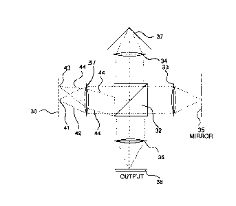
FIG. 4 shows the optical setup that inl.plements the first crossover stage of our
network employing the principles of our invention. At the heart of the stage is beam
splitter cube 32 which also serves as a beam combiner, mirror 35, and prismatic mirror 37
which provides the crossover capability. Describing the arrangement in detail, the input
image array is available at plane 3Q and the light emanating from the input array is
passed through lens 31 and applied to beam splitter 32. Lens 31 is arranged at one focal
length away from input plane 30 and that causes lens 31 to collimate the light of the
image, as illustrated in FIG. 4 by light rays 42 coming from point 41 on the input plane,
and light rays 44 coming from point 43 on the input plane. Element 32 splits the input
image array into two copies, with one copy moving into lens 33, and the other copy
moving into lens 34. At one focal distance away from lens 33 the beam is focused onto
ftat mirror 35 and is reflected off the mirror and reapplied to lens 33 and beam sptitter 32.
This re-entering beam is split again, with one copy being directed to lens 36, and the other
copy being directed to lens 31.
A prismatic mirror 37 faces lens 34, with its corner set at one focal length
away from the lens. The prismatic mirror reflects the incoming array back to
lens 34 but in the process it reverses the image portion encompassed by the mirror.
The reversal is about the axis formed by thc corner. The reversed and
.
~3~3~
- 5 -
reflected image passes through lens 34, enters beam splitter 32 and splits into two
copies~ One copy continues to lens 36, while the other copy is deflectçd to lens31. The two beams arriving at lens 36 ~lre combined at output plane 38, which islocated one focal length away from lens 36. Thus, beam splitter 32 acts as a
5 combiner, albeit a lossy one. Of course, output plane 38 may be connected to
some udlizadon element, as dcscribed infra, or may comprise the input to anotherstage.
The reversal that is achieved by prismatic rnirror 37 can be observed
more clearly in FIGS. S and 6. In FIG. 5, a collimated incoming beam is shown
10 by rays 45 and 46. These rays, as well as the rays between them, pass throughlens 34 and are focused on point P. In the absence of mi~ror 37 and the presenceof a flat rnirror at point P, rays 45 and 46 would be returned to lens 34 as rays 47
and 48. However, the rays do not reach point P because they are deflected twice
by prismatic mirror 37 and returned to lens 34 as rays 49 and 50. With prismadc
15 mirror 37 in place, what results is a shift of the image point P to the virtual image
point P'. By analogy, one can easily see that an incoming beam along rays 49
and 50 is reflected and deflected so tha~ the returning ~eam appears to emanate not
from point P' but from point P.
I~us, prismadc rnirror 37 simply spli~s the image along the line of its
20 corner, and performs a horizontal ~ansposition. The effec~ is a reversal of the
entire image encompassed by the prismatic mirror about the axis corresponding toits corner. The effect of this action is shown on the image of the numeral 4,
depicted in FIG. 6.
It may be noted that the crossover stage of FIG. 4 exhibits light loss
25 because the second pass through the beam splitter causes half of the light to return
to lens 31. However, if one were to use a polarizing bearn splitter in combination
with quarter-wave plates in the two branches, no light loss would occur. FIG. 7
illustrates such a system. Specifically, the FIG. 7 crossover network employs a
circularly polarized light at input plane 30, and a polarizing beam splitter 52 that
30 deflects the y-polarized portion of the beam while passing the x-polarized portion
of the beam. The path leading to lens 34 contains the y-polarized, and the path
leading to lens 33 contains the x-polarized portion of the beam. At the two outputs
of the beam splitter that lead to lens 33 and 34, a quarter-wave plate 54 is
included, and it converts the x and y polariæd light to circular-polarized light.
35 Upon return of the beams from mirrors 35 and 37, the quarter-wave plates convert
the polarization of the beams again, and the result is that the previously
~3~37~
- 6 -
x-polarized light is now y-polarized, and vice versa. Beam splitter 5~ deflects the
y-polarized light derived from mirror 35 and passes the 1c-polarized light derived
from prismatic mirror 37, yielding the desired combining of images at the outputplane, essentially without any loss of light.
S In some applications, the polarization of the light at the output plane
is unimportant. In other applications, however, one may wish to have the same
polarization for the direct and the crossover output images. If the input image
comprises a plurality of distinct pixels with black regions between the pixels, one
can arrange for the two images formed on the output plane to be offest from each10 other. Indeed, in most applications such a physical offset is desirable. Having
such an offset, we employ a space-variant half-wave plate at the output plane tocause both images to be polarized in the same direction (e.g., y-polarized). This
is shown in FIG. 7 by equalization element 55. If necessary or desirable, a
quarter-wave plate following the space-variant element 55 would bring the image
15 at the output plane to the same polarization state that the input had. This last
quarter-wave plate is not shown in FIG. 7.
In many applications some operations are performed at the output
plane of every stage. 'rhis may include mere switching or actual computations.
In fact, both functions can be accomplished using SEED devices. For a
20 description of SEED devices one may tum to US Patent 4,546,244 issued to D. A.
B. Miller on October 8, 1985. SEED devices are optical devices that are
responsive to two optical signals, and based on those signals, the SEED dPvices
either absorb or reflect a "power supply" beam. The logic function that can be
realized is OR or NOR, which allows the power supply beam to be reflected when
25 any one of ~e signal bearns is present, or when none of dle signal beams are
present. The reflected power supply beam possesses ehe same polarization as ehe
incoming power supply beam.
- The issue of supplying the power supply beam to the SEED devices
and also observing the reflected power supply beam is a matter that must be
30 addressed in our crossover network, if we are to use SEED devices. As shown in
FIG. 8, one approach that can be employed is to follow the space-vanant half-
wave plate 55 with a collimating lens 58 and apply the resulting bearn to a
polarizing beam splitter 59 that interacts through lens 56 with plane 60 on which
the SEED devices are placed. If the polarization of the beam entering beam
35 splitter 59 (from equalization element 55) is in the y direcdon, then the beam is
deflected and, therefore, the SEED devices plane is plnced perpendiculnrly to lens
7 ~32~3~
58. 'rhe power supply beam can then be applied, with x-polaTization, from the
other side of bearn splitter 59, opposite the SEED device~s plane. The x-polarized
reflected power supply beam contains the information of the crossover stage but it
returns towards the incoming power supply beam.
S To distinguish the reflected power supply beam (which is the
modulated signal beam from the SEED array) from the applied pc>wer supply
beam, an additional beam splitter (61) is included in FIG. 8. Associated with
splitter 61 there is a quarter-wave plate 62 facing beam splitter 59, and a quarter-
wave plate 63 facing the power supply source. In this manner, a linearly
10 polanzed light source (e.g., a laser) is collimated in lens 64, is converted to
circularly polarized light in quarter-wave plate 63, is passed through beam splitter
61 and through quarter-wave plate 62, and results in being x-polarized as desired,
prior to entry into beam splitter 59. The returning x-polarized bearn is also
converted to circular polarization by quarter-wave plate 62 and is split within
15 beam splitter 61. This arrangement results in separation of the applied powersupply beam and the reflected power supply beam. However, this arrangement
also results in a double loss of light; once when the power supply beam passes
through beam splitter 61, and once when the reflected power supply beam again
passes through beam splitter 61.
It may be noted in passing that the power supply light source is not a
single beam but, rather, a collection of light spots of precise posidoning (to meet
the SEED devices at the appropriate locations) and of essentially equal light
intensity.
A much better realization is achieved, in acco~dance with our
25 invention, with the setup depicted in FIG. 9, where the power supply beam is
generated in element 70. The power supply beam, comprising an array of spots,
can be obtained by the use of a collimated laser beam that is passed through a
lenslet array or a Dammann binary phase grading followed by a Fourier lens.
Such a system is shown, for exarnple, in Offenlegungsschrift 26-08-176, dated
30 September 1,1977.
In FIG. 9, the power supply beam is generated in element 70 and
arranged to focus its light spots onto element 35'. Element 35' serves the
function of mirror 35 in FIG. 4, except that it is arranged to be reflective only
where necessary, i.e., at the locations where the pixels of the input image appear
35 at the element. At other locations element 35' is transparent, and element 70 is
arranged to focus its light spots at the transparent regions. The light of element
-8- ~32~370
70 must of course be of the appropriate polarization mode, to wit, the same
polarization as the light reflected off mirror 35' ~circular polarization). Also, this
setup assumes that the input array that is reflected off milror 35' comprises a
collection of spots and no information in between.
S In the FIG. 9 arrangement, the collimated output of lens 58, which
contains the two image beams and the power supply be~, is applied to a beam
splitter 59. Since all of the applied light signals applied are of y-polarizadon, they
are deflected onto SEED plate 60 through quarter-wave jplate 65 and lens 56.
Plate 65 causes reflected power supply beam signals to be polarized in the
10 x-direction upon their re-en~ry into beam splitter 59. With this polarization, the
light signals pass without deflection to quarter-wave plate 66~ which returns the
light signals to the same polarization that they had at the input plane. That light
may then be ~ocused onto an output place via lens 57.
The implementation of higher stages of the network can be
15 accomplished with the same setup as shown in FIG. 4, except that the number of
corners in the prismatic mirror would be dif~erent for different stages of the
network. Each succeeding stage has a number of corners in the prismatic rni~ror
that is twice as large as the number of corners in the prismatic mirror of the
preceding stage. Such different stages, and an arrangement interconnecting ehe
20 stages are shown in FIG. 10, which depicts one embodiment for a three stage
crossover network.
A number of salient features of the FIG. 10 embodiment may be
noted. First, each stage comprises the same number of elements, and
eorresponding elements are identical to each other, except the prismatic mirrors.
25 Second, between each stage the~e is a processing element 71. Each element 71 is
functionally sim~lar as the other elements 71. The switching or computation thatis performed in the network is performed within elemçnts 71. Third, the lenses at
the input and output planes (31 and 36) are subsumed within elements 71. It may
be noted in passing that a rigorous application of the teachings herein may result,
30 in some cases, in the use of two lenses in succession, which in effect serve merely
to reverse the image. In many applications there is no need to keep track of theorientation, since it is the relative positions of pixels that is important. Fourth, the
positions of input and output image planes in FIG. 10 lend themselves to easy
cascading of additional stages.
9 1~2~
The above description and the drawings are illustradve of our
invention, and the skilled artisan can easily envision different embodiments that
employ the principles of our invendon. For example, though we described the use
for the sarne element as the beam spl}tter and the combiner, it is clear that
S different elements can be employed. Further, the image reversing means can be
other than a prismatic m~rror, such as lens (one or two dimensions) arrangements.
Sdll further, with a rearrangement of the FIG. 2 crossover network as shown, forexample, in FIG. 11, a crossover stage as depicted in FIG. 12 can be employed.